EP0780672B1 - Field effect controllable semiconductor device with temperature sensor - Google Patents
Field effect controllable semiconductor device with temperature sensor Download PDFInfo
- Publication number
- EP0780672B1 EP0780672B1 EP96119029A EP96119029A EP0780672B1 EP 0780672 B1 EP0780672 B1 EP 0780672B1 EP 96119029 A EP96119029 A EP 96119029A EP 96119029 A EP96119029 A EP 96119029A EP 0780672 B1 EP0780672 B1 EP 0780672B1
- Authority
- EP
- European Patent Office
- Prior art keywords
- zone
- semi
- conductor device
- bipolar transistor
- temperature sensor
- Prior art date
- Legal status (The legal status is an assumption and is not a legal conclusion. Google has not performed a legal analysis and makes no representation as to the accuracy of the status listed.)
- Expired - Lifetime
Links
- 239000004065 semiconductor Substances 0.000 title claims description 61
- 230000005669 field effect Effects 0.000 title claims description 4
- 230000001419 dependent effect Effects 0.000 claims description 4
- 229910021420 polycrystalline silicon Inorganic materials 0.000 claims 1
- 229920005591 polysilicon Polymers 0.000 claims 1
- 238000009792 diffusion process Methods 0.000 description 9
- 239000002800 charge carrier Substances 0.000 description 2
- 238000001514 detection method Methods 0.000 description 2
- 230000007704 transition Effects 0.000 description 2
- 230000007423 decrease Effects 0.000 description 1
- 230000000694 effects Effects 0.000 description 1
- 230000002349 favourable effect Effects 0.000 description 1
Images
Classifications
-
- H—ELECTRICITY
- H01—ELECTRIC ELEMENTS
- H01L—SEMICONDUCTOR DEVICES NOT COVERED BY CLASS H10
- H01L29/00—Semiconductor devices adapted for rectifying, amplifying, oscillating or switching, or capacitors or resistors with at least one potential-jump barrier or surface barrier, e.g. PN junction depletion layer or carrier concentration layer; Details of semiconductor bodies or of electrodes thereof ; Multistep manufacturing processes therefor
- H01L29/66—Types of semiconductor device ; Multistep manufacturing processes therefor
- H01L29/68—Types of semiconductor device ; Multistep manufacturing processes therefor controllable by only the electric current supplied, or only the electric potential applied, to an electrode which does not carry the current to be rectified, amplified or switched
- H01L29/70—Bipolar devices
- H01L29/72—Transistor-type devices, i.e. able to continuously respond to applied control signals
- H01L29/739—Transistor-type devices, i.e. able to continuously respond to applied control signals controlled by field-effect, e.g. bipolar static induction transistors [BSIT]
-
- G—PHYSICS
- G01—MEASURING; TESTING
- G01K—MEASURING TEMPERATURE; MEASURING QUANTITY OF HEAT; THERMALLY-SENSITIVE ELEMENTS NOT OTHERWISE PROVIDED FOR
- G01K7/00—Measuring temperature based on the use of electric or magnetic elements directly sensitive to heat ; Power supply therefor, e.g. using thermoelectric elements
- G01K7/01—Measuring temperature based on the use of electric or magnetic elements directly sensitive to heat ; Power supply therefor, e.g. using thermoelectric elements using semiconducting elements having PN junctions
-
- H—ELECTRICITY
- H01—ELECTRIC ELEMENTS
- H01L—SEMICONDUCTOR DEVICES NOT COVERED BY CLASS H10
- H01L29/00—Semiconductor devices adapted for rectifying, amplifying, oscillating or switching, or capacitors or resistors with at least one potential-jump barrier or surface barrier, e.g. PN junction depletion layer or carrier concentration layer; Details of semiconductor bodies or of electrodes thereof ; Multistep manufacturing processes therefor
- H01L29/66—Types of semiconductor device ; Multistep manufacturing processes therefor
- H01L29/66007—Multistep manufacturing processes
- H01L29/66075—Multistep manufacturing processes of devices having semiconductor bodies comprising group 14 or group 13/15 materials
- H01L29/66227—Multistep manufacturing processes of devices having semiconductor bodies comprising group 14 or group 13/15 materials the devices being controllable only by the electric current supplied or the electric potential applied, to an electrode which does not carry the current to be rectified, amplified or switched, e.g. three-terminal devices
- H01L29/66234—Bipolar junction transistors [BJT]
- H01L29/66325—Bipolar junction transistors [BJT] controlled by field-effect, e.g. insulated gate bipolar transistors [IGBT]
-
- H—ELECTRICITY
- H01—ELECTRIC ELEMENTS
- H01L—SEMICONDUCTOR DEVICES NOT COVERED BY CLASS H10
- H01L29/00—Semiconductor devices adapted for rectifying, amplifying, oscillating or switching, or capacitors or resistors with at least one potential-jump barrier or surface barrier, e.g. PN junction depletion layer or carrier concentration layer; Details of semiconductor bodies or of electrodes thereof ; Multistep manufacturing processes therefor
- H01L29/66—Types of semiconductor device ; Multistep manufacturing processes therefor
- H01L29/68—Types of semiconductor device ; Multistep manufacturing processes therefor controllable by only the electric current supplied, or only the electric potential applied, to an electrode which does not carry the current to be rectified, amplified or switched
- H01L29/76—Unipolar devices, e.g. field effect transistors
- H01L29/772—Field effect transistors
- H01L29/78—Field effect transistors with field effect produced by an insulated gate
- H01L29/7801—DMOS transistors, i.e. MISFETs with a channel accommodating body or base region adjoining a drain drift region
- H01L29/7802—Vertical DMOS transistors, i.e. VDMOS transistors
-
- H—ELECTRICITY
- H01—ELECTRIC ELEMENTS
- H01L—SEMICONDUCTOR DEVICES NOT COVERED BY CLASS H10
- H01L29/00—Semiconductor devices adapted for rectifying, amplifying, oscillating or switching, or capacitors or resistors with at least one potential-jump barrier or surface barrier, e.g. PN junction depletion layer or carrier concentration layer; Details of semiconductor bodies or of electrodes thereof ; Multistep manufacturing processes therefor
- H01L29/02—Semiconductor bodies ; Multistep manufacturing processes therefor
- H01L29/06—Semiconductor bodies ; Multistep manufacturing processes therefor characterised by their shape; characterised by the shapes, relative sizes, or dispositions of the semiconductor regions ; characterised by the concentration or distribution of impurities within semiconductor regions
- H01L29/0603—Semiconductor bodies ; Multistep manufacturing processes therefor characterised by their shape; characterised by the shapes, relative sizes, or dispositions of the semiconductor regions ; characterised by the concentration or distribution of impurities within semiconductor regions characterised by particular constructional design considerations, e.g. for preventing surface leakage, for controlling electric field concentration or for internal isolations regions
- H01L29/0607—Semiconductor bodies ; Multistep manufacturing processes therefor characterised by their shape; characterised by the shapes, relative sizes, or dispositions of the semiconductor regions ; characterised by the concentration or distribution of impurities within semiconductor regions characterised by particular constructional design considerations, e.g. for preventing surface leakage, for controlling electric field concentration or for internal isolations regions for preventing surface leakage or controlling electric field concentration
- H01L29/0611—Semiconductor bodies ; Multistep manufacturing processes therefor characterised by their shape; characterised by the shapes, relative sizes, or dispositions of the semiconductor regions ; characterised by the concentration or distribution of impurities within semiconductor regions characterised by particular constructional design considerations, e.g. for preventing surface leakage, for controlling electric field concentration or for internal isolations regions for preventing surface leakage or controlling electric field concentration for increasing or controlling the breakdown voltage of reverse biased devices
- H01L29/0615—Semiconductor bodies ; Multistep manufacturing processes therefor characterised by their shape; characterised by the shapes, relative sizes, or dispositions of the semiconductor regions ; characterised by the concentration or distribution of impurities within semiconductor regions characterised by particular constructional design considerations, e.g. for preventing surface leakage, for controlling electric field concentration or for internal isolations regions for preventing surface leakage or controlling electric field concentration for increasing or controlling the breakdown voltage of reverse biased devices by the doping profile or the shape or the arrangement of the PN junction, or with supplementary regions, e.g. junction termination extension [JTE]
- H01L29/0619—Semiconductor bodies ; Multistep manufacturing processes therefor characterised by their shape; characterised by the shapes, relative sizes, or dispositions of the semiconductor regions ; characterised by the concentration or distribution of impurities within semiconductor regions characterised by particular constructional design considerations, e.g. for preventing surface leakage, for controlling electric field concentration or for internal isolations regions for preventing surface leakage or controlling electric field concentration for increasing or controlling the breakdown voltage of reverse biased devices by the doping profile or the shape or the arrangement of the PN junction, or with supplementary regions, e.g. junction termination extension [JTE] with a supplementary region doped oppositely to or in rectifying contact with the semiconductor containing or contacting region, e.g. guard rings with PN or Schottky junction
-
- H—ELECTRICITY
- H01—ELECTRIC ELEMENTS
- H01L—SEMICONDUCTOR DEVICES NOT COVERED BY CLASS H10
- H01L29/00—Semiconductor devices adapted for rectifying, amplifying, oscillating or switching, or capacitors or resistors with at least one potential-jump barrier or surface barrier, e.g. PN junction depletion layer or carrier concentration layer; Details of semiconductor bodies or of electrodes thereof ; Multistep manufacturing processes therefor
- H01L29/40—Electrodes ; Multistep manufacturing processes therefor
- H01L29/402—Field plates
Definitions
- Power semiconductor devices of the type mentioned are e.g. in the form of so-called SMART-FET on the market.
- the principle of one Temperature sensor of the type mentioned is e.g. in the EP 0 240 807.
- the temperature sensor contains a reverse polarity bipolar transistor, the one as Constant current source switched depletion FET connected in series is. This temperature sensor is thermal with the Power semiconductor device coupled by the fact that it adjacent, e.g. arranged in a recess of the cell field is.
- the current of the constant current source is now set so that it is higher than the reverse current of the bipolar transistor, at the normal operating temperature of the power semiconductor device flows. However, it is lower than that Reverse current, the overtemperature of the power semiconductor device flows. At the transition from normal operating temperature Excess temperature then occurs at the depletion MOSFET a pronounced increase in voltage, which is the overtemperature signaled.
- the temperature sensor can be a chip on the semiconductor body of the power semiconductor component are mounted or becomes Monolithically integrated in the same semiconductor body.
- the basic zone is the monolithically integrated solution of the bipolar transistor and the gate zones of the power semiconductor component of the same line type.
- the collector zone of the bipolar transistor and the drain zone of the Power semiconductor device are through a single zone of the semiconductor body of the power semiconductor component educated.
- the current of the reverse bipolar transistor by increasing the temperature of the Power semiconductor device larger.
- This current continues resulting from the actual reverse current of the bipolar transistor and a diffusion current by the difference in concentration the minority charge carrier between the Boundary of the space charge zone of the power semiconductor component on the one hand and the boundary of the space charge zone of the bipolar transistor on the other hand is generated.
- This diffusion current is not only temperature dependent, but also also depends on the potential of the source connection of the power semiconductor component from.
- the size of the diffusion current therefore also affected by whether the load is in normal condition is short-circuited in whole or in part.
- the transistor current is not only temperature-dependent, but also depending on the load. A perfect detection of the overtemperature is not possible with it.
- EP 0 550 850 A2 describes a vertical power transistor with a monolithically integrated temperature sensor, which consists of two sensor cells, which together with the Power transistor can be produced, being in the range of Sensor cells a lateral bipolar transistor is formed.
- US 5,237,481 describes a power transistor with a monolithically integrated diode arrangement that acts as a temperature sensor serves.
- the invention has for its object a field effect controllable power semiconductor device of the described Kind in such a way that the temperature detection independently from the source potential of the power semiconductor component is.
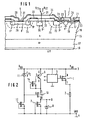
- the power semiconductor component according to Figure 1 has one Semiconductor body 15 with a weakly n-doped drain zone 16. A heavily n-doped zone 17, whose Surface is contacted by a drain electrode 18. A p-doped is in the other surface of the semiconductor body Gate zone 20 embedded, in turn a strong n-doped source zone 21 is embedded. The gate zone is covered by a gate electrode 23 on an insulating layer is arranged. The gate zone 20 and the source zone 21 is contacted by a source electrode 24. She is with a source connection S connected.
- the gate zone 20 and the source zone 21 form a cell of the Power semiconductor component.
- On the semiconductor body a plurality of cells are arranged. All cells are connected in parallel by the source electrode 24.
- the gate electrode 23 is also common to all cells.
- the drain zone of all cells is through zone 16 of the semiconductor body 15 formed.
- An edge cell is arranged adjacent to the cell shown, which consists of a gate zone 22 and a source zone 21. These zones are also contacted by the source electrode 24.
- the gate zone 22 is deeper than the gate zone 20, this is in conjunction with the illustrated Field electrode in a known manner a favorable course the space charge zone on the surface of the semiconductor body set.
- the zones mentioned form a power MOSFET.
- a p-doped base zone 26 into which again an n-doped emitter zone 27 is embedded.
- the emitter zone is contacted by an emitter electrode 28.
- a p-doped zone 30 is embedded. This zone is contacted and with a connection 31 connected to a fixed or optionally different fixed prestresses can be applied.
- the distance between the zone 30 and the bipolar transistor 6 on the one hand and between the zone 30 and the power semiconductor device 1 on the other hand is chosen so that its by the dashed Lines limited space charge zones 35 and 25 do not match the Encounter zone 30.
- Zone 30 is expediently of the same depth and doped to the same extent as the deep part of the base zone 22.
- the p-doped zone 30 is not present.
- the source V of 1 has the potential V bb .
- the pn junction between zones 16 and 22 is thus not blocked and the minority carrier charge density is therefore at its edge in thermal equilibrium (p no ) and only dependent on the temperature.
- the pn junction of the bipolar transistor between zones 26 and 16 is reverse biased, the minority carrier charge density is therefore reduced here. Due to the concentration gradient, a diffusion current flows from the edge of the space charge zone 35 into the bipolar transistor 6.
- the source potential decreases by 1 e.g. through a Short circuit of load 2
- the pn transition between 22nd and 16 polarized in the reverse direction and the minority carrier charge density is lowered at the edge of the space charge zone 25.
- the distance between the p-regions 22 and 26 is of the order of magnitude the diffusion length, so becomes the minority carrier charge density lowered in the entire range between 22 and 26.
- the diffusion current thus drops into the bipolar transistor 6 depending on the source potential at 1 and an overtemperature could not be clearly recorded.
- zone 30 which is connected to a fixed bias. If zone 30 is at potential V bb , for example, a density of minority charge carriers is established at its pn junction, which corresponds to the thermal equilibrium. At the edge of the biased pn junction between the zones 26 and 16, the density is reduced, and therefore a diffusion current flows into the bipolar transistor 6 as described above is also in thermal equilibrium between 30 and the space charge zone 35, the diffusion current into the bipolar transistor 6 is independent of the source potential at the power semiconductor component 1.
- zone 30 can still be improved by that the surface of the semiconductor body between the zone 30 and the base zone 26 is covered with a field electrode 33, which in turn is arranged on an insulating layer 32.
- the field electrode 33 can in turn be covered by an insulating layer 34 may be covered on which the emitter electrode 28 and the source electrode 24 is located.
- the field electrode 33 can either with the zone 30 or with the base zone 26 electrically be connected. This makes it possible to tap the potential at the Adjust surface of the semiconductor body. It depends on the field electrodes 33 with the zone 30 or with the base zone 26 is connected, the zone sequence 26, 16, 30 acts as a MOS diode or as a blocked transistor.
- Zone 30 can, instead of being connected to only a single fixed bias voltage, optionally also to several, here to two, fixed bias voltages U f1 , U f2 of different heights.
- the level of the diffusion current can thus be adjusted. It applies that the response threshold of the temperature sensor is shifted towards higher temperatures with a lower pretension, whereas it is shifted towards lower temperatures with a higher pretension.
- By switching the bias voltages it is therefore possible to set a switching hysteresis of the temperature sensor.
- the circuit arrangement according to FIG. 2 contains the power semiconductor component 1 and the temperature sensor with the bipolar transistor 6.
- the bipolar transistor 6 is on the emitter side a p-channel MOSFET 10 and a current source 7 connected in series.
- the current source advantageously consists of a Depletion-FET, whose gate connection with the source connection connected is.
- a Zener diode 8 is connected in parallel.
- the node between MOSFET 7 and 10 is with an output 9 connected.
- the series connection from 6, 10 and 7 is the series connection from a Zener diode 11 and a second, as Power source switched depletion-FET 12 connected in parallel.
- the node between 11 and 12 is connected to the gate terminal G of 10 connected.
- the Bipolar transistor which is dimensioned so that it is at a normal temperature flowing base current forms a short circuit, however becomes high resistance above this temperature.
- the Temperature sensor insensitive to faults e.g. by Voltage fluctuations.
- the power semiconductor device 1 is a power MOSFET.
- a load 2 is connected in series at the source. It is controlled by a control circuit 5, the output of which is connected to the gate terminal of FIG. 1.
- the circuit which is described in principle, for example, in US Pat. No. 4,875,131, has the following mode of operation:
- the gate connection of 10 is connected to a constant potential V bb -U Z via the diode 11 and the MOSFET 12.
- a constant voltage U Z -V th10 is then present at the bipolar transistor 6.
- the depletion FET 7 is dimensioned such that its saturation current at normal operating temperature of the semiconductor component 1 is greater than the reverse current of the bipolar transistor 6.
- the potential at the output 9 is then approximately at ground potential.
- the reverse current of the bipolar transistor 6 increases exponentially with the temperature.
- the reverse current of the bipolar transistor 6 exceeds the saturation current of the MOSFET 7.
- a voltage rise thus occurs at the output 9, which indicates overtemperature.
- the voltage is limited by the Zener diode 8.
- the invention is independent of that shown in Figure 2 Circuitry integrated anywhere in monolithic Circuits to use.
- the invention can also be used for IGBT. It is the heavily n-doped zone 17 in the region of the MOSFET 1 replaced a heavily p-doped zone.
Description
Die Erfindung bezieht sich auf ein durch Feldeffekt steuerbares,
eine Vielzahl von einander parallel geschalteten Zellen
aufweisendes Leistungs-Halbleiterbauelement mit einem einen
Bipolartransistor enthaltenden Temperatursensor, der dem Zellenfeld
des Leistungs-Halbleiterbauelementes benachbart angeordnet
ist, mit den Merkmalen:
Leistungs-Halbleiterbauelemente der genannten Art sind z.B. in Form sogenannter SMART-FET auf dem Markt. Das Prinzip eines Temperatursensors der genannten Art ist z.B. in der EP 0 240 807 beschrieben worden. Der Temperatursensor enthält einen in Sperrichtung gepolten Bipolartransistor, dem ein als Konstantstromquelle geschalteter Depletion-FET in Reihe geschaltet ist. Dieser Temperatursensor ist thermisch mit dem Leistungs-Halbleiterbauelementes dadurch gekoppelt, daß er benachbart, z.B. in einer Aussparung des Zellenfeldes angeordnet ist.Power semiconductor devices of the type mentioned are e.g. in the form of so-called SMART-FET on the market. The principle of one Temperature sensor of the type mentioned is e.g. in the EP 0 240 807. The temperature sensor contains a reverse polarity bipolar transistor, the one as Constant current source switched depletion FET connected in series is. This temperature sensor is thermal with the Power semiconductor device coupled by the fact that it adjacent, e.g. arranged in a recess of the cell field is.
Der Strom der Konstantstromquelle ist nun so eingestellt, daß er höher ist als derjenige Sperrstrom des Bipolartransistors, der bei der normalen Betriebstemperatur des Leistungs-Halbleiterbauelementes fließt. Er ist jedoch niedriger als derjenige Sperrstrom, der bei Übertemperatur des Leistungs-Halbleiterbauelementes fließt. Beim Übergang von normaler Betriebstemperatur auf Übertemperatur tritt dann am Depletion-MOSFET ein ausgeprägter Spannungsanstieg ein, der die Übertemperatur signalisiert.The current of the constant current source is now set so that it is higher than the reverse current of the bipolar transistor, at the normal operating temperature of the power semiconductor device flows. However, it is lower than that Reverse current, the overtemperature of the power semiconductor device flows. At the transition from normal operating temperature Excess temperature then occurs at the depletion MOSFET a pronounced increase in voltage, which is the overtemperature signaled.
Der Temperatursensor kann als Chip auf dem Halbleiterkörper des Leistungs-Halbleiterbauelementes montiert werden oder erwird im gleichen Halbleiterkörper monolithisch integriert. Bei der monolithisch integrierten Lösung sind die Basiszone des Bipolartransistors und die Gatezonen des Leistungs-Halbleiterbauelementes vom gleichen Leitungstyp. Die Kollektorzone des Bipolartransistors und die Drainzone des Leistungs-Halbleiterbauelementes sind durch eine einzige Zone des Halbleiterkörpers des Leistungs-Halbleiterbauelementes gebildet.The temperature sensor can be a chip on the semiconductor body of the power semiconductor component are mounted or becomes Monolithically integrated in the same semiconductor body. The basic zone is the monolithically integrated solution of the bipolar transistor and the gate zones of the power semiconductor component of the same line type. The collector zone of the bipolar transistor and the drain zone of the Power semiconductor device are through a single zone of the semiconductor body of the power semiconductor component educated.
Wie erwähnt, wird der Strom des in Sperrichtung gepolten Bipolartransistors durch die Erhöhung der Temperatur des Leistungs-Halbleiterbauelementes größer. Dieser Strom setzt sich aus dem eigentlichen Sperrstrom des Bipolartransistors und einem Diffusionsstrom zusammen, der durch den Konzentrationsunterschied der Minoritätsladungsträger zwischen der Grenz der Raumladungszone des Leistungs-Halbleiterbauelementes einerseits und der Grenze der Raumladungszone des Bipolartransistors andererseits erzeugt wird. Dieser Diffusionsstrom ist damit nicht nur temperaturabhängig, sondern hängt auch vom Potential des Sourceanschlusses des Leistungs-Halbleiterbauelementes ab. Bei Leistungs-Halbleiterbauelementen mit sourceseitiger Last wird die Größe des Diffusionsstroms daher auch davon beeinflußt, ob die Last im Normalzustand ist oder ganz oder teilweise kurzgeschlossen ist. Damit wird der Transistorstrom nicht nur temperaturabhängig, sondern auch lastabhängig. Eine einwandfreie Erfassung der Übertemperatur ist damit nicht möglich.As mentioned, the current of the reverse bipolar transistor by increasing the temperature of the Power semiconductor device larger. This current continues resulting from the actual reverse current of the bipolar transistor and a diffusion current by the difference in concentration the minority charge carrier between the Boundary of the space charge zone of the power semiconductor component on the one hand and the boundary of the space charge zone of the bipolar transistor on the other hand is generated. This diffusion current is not only temperature dependent, but also also depends on the potential of the source connection of the power semiconductor component from. For power semiconductor devices with load on the source, the size of the diffusion current therefore also affected by whether the load is in normal condition is short-circuited in whole or in part. In order to the transistor current is not only temperature-dependent, but also depending on the load. A perfect detection of the overtemperature is not possible with it.
Die EP 0 550 850 A2 beschreibt einen vertikalen Leistungstransistor mit einem monolithisch integrierten Temperatursensor, der aus zwei Sensorzellen besteht, die zusammen mit dem Leistungstransistor herstellbar sind, wobei im Bereich der Sensorzellen ein lateraler Bipolartransistor gebildet ist.EP 0 550 850 A2 describes a vertical power transistor with a monolithically integrated temperature sensor, which consists of two sensor cells, which together with the Power transistor can be produced, being in the range of Sensor cells a lateral bipolar transistor is formed.
Die US 5,237,481 beschreibt einen Leistungstransistor mit einem monolithisch integrierten Diodenanordnung, die als Temperatursensor dient.US 5,237,481 describes a power transistor with a monolithically integrated diode arrangement that acts as a temperature sensor serves.
Der Erfindung liegt die Aufgabe zugrunde, ein durch Feldeffekt steuerbares Leistungs-Halbleiterbauelement der beschriebenen Art so weiterzubilden, daß die Temperaturerfassung unabhängig vom Source-Potential des Leistungs-Halbleiterbauelements ist.The invention has for its object a field effect controllable power semiconductor device of the described Kind in such a way that the temperature detection independently from the source potential of the power semiconductor component is.
Dieses Ziel wird durch ein Halbleiterbauelement gemäß den Merkmalen des Anspruchs 1 gelöst. This goal is achieved by a semiconductor device according to the Features of claim 1 solved.
Die Erfindung wird anhand eines Ausführungsbeispiels in Verbindung mit den Figuren 1 und 2 näher erläutert. Es zeigen
- Figur 1
- den Schnitt durch ein erfindungsgemäßes Leistungs-Halbleiterbauelement und
- Figur 2
- die Schaltungsanordnung eines bekannten Temperatursensors zur Erfassung der Übertemperatur eines Leistungs-Halbleiterbauelementes 1, in der die Erfindung angewendet werden kann.
- Figure 1
- the section through an inventive power semiconductor device and
- Figure 2
- the circuit arrangement of a known temperature sensor for detecting the excess temperature of a power semiconductor component 1, in which the invention can be applied.
Das Leistungs-Halbleiterbauelement nach Figur 1 hat einen
Halbleiterkörper 15 mit einer schwach n-dotierten Drainzone
16. An die Zone 16 grenzt eine stark n-dotierte Zone 17, deren
Oberfläche durch eine Drainelektrode 18 kontaktiert ist.
In die andere Oberfläche des Halbleiterkörpers ist eine p-dotierte
Gatezone 20 eingebettet, in die wiederum eine stark
n-dotierte Sourcezone 21 eingebettet ist. Die Gatezone ist
von einer Gateelektrode 23 überdeckt, die auf einer Isolierschicht
angeordnet ist. Die Gatezone 20 und die Sourcezone 21
ist durch eine Sourceelektrode 24 kontaktiert. Sie ist mit
einem Sourceanschluß S verbunden.The power semiconductor component according to Figure 1 has one
Die Gatezone 20 und die Sourcezone 21 bildet eine Zelle des
Leistungs-Halbleiterbauelementes. Auf dem Halbleiterkörper
ist eine Vielzahl von Zellen angeordnet. Alle Zellen sind
einander durch die Sourceelektrode 24 parallel geschaltet.
Die Gateelektrode 23 ist ebenfalls allen Zellen gemeinsam. The
Die Drainzone aller Zellen wird durch die Zone 16 des Halbleiterkörpers
15 gebildet.The drain zone of all cells is through
Benachbart der gezeigten Zelle ist eine Randzelle angeordnet,
die aus einer Gatezone 22 und einer Sourcezone 21 besteht.
Auch diese Zonen sind durch die Sourceelektrode 24 kontaktiert.
Die Gatezone 22 ist tiefer als die Gatezone 20 ausgebildet,
hierdurch wird in Verbindung mit der dargestellten
Feldelektrode auf bekannte Art und Weise ein günstiger Verlauf
der Raumladungszone an der Oberfläche des Halbleiterkörpers
eingestellt. Die genannten Zonen bilden einen Leistungs-MOSFET.An edge cell is arranged adjacent to the cell shown,
which consists of a
In die sourceseitige Oberfläche des Halbleiterkörpers 15 ist
außerdem eine p-dotierte Basiszone 26 eingebettet, in die
wiederum eine n-dotierte Emitterzone 27 eingebettet ist. Die
Emitterzone ist durch eine Emitterelektrode 28 kontaktiert.
Diese Zonen bilden zusammen mit der Zone 16 als Kollektorzone
einen Bipolartransistor, der mit 6 bezeichnet ist.In the source-side surface of the
Zwischen dem Leistungs-Halbleiterbauelement 1 und dem Bipolartransistor
6 ist in die source- bzw. emitterseitige Oberfläche
des Halbleiterkörpers 15 eine p-dotierte Zone 30 eingebettet.
Diese Zone ist kontaktiert und mit einem Anschluß
31 verbunden, an den eine feste oder wahlweise unterschiedliche
feste Vorspannungen anlegbar sind. Der Abstand zwischen
der Zone 30 und dem Bipolartransistor 6 einerseits und zwischen
der Zone 30 und dem Leistungs-Halbleiterbauelement 1
andererseits ist so gewählt, daß ihre durch die gestrichelten
Linien begrenzten Raumladungszonen 35 bzw. 25 nicht an die
Zone 30 stoßen. Die Zone 30 ist zweckmäßigerweise gleich tief
und gleich stark dotiert wie der tiefe Teil der Basiszone 22.Between the power semiconductor device 1 and the
Zur Erläuterung der Wirkungsweise der Anordnung wird zunächst
davon ausgegangen, daß die p-dotierte Zone 30 nicht vorhanden
ist. Bei eingeschaltetem Leistungs-Halbleiterbauelement 1 und
Normalzustand der Last 2 liegt am Sourceanschluß von 1 das
Potential Vbb. Der pn-Übergang zwischen den Zonen 16 und 22
ist damit nicht gesperrt und die Minoritätsträger-Ladungsdichte
ist an seiner Kante damit im thermischen Gleichgewicht
(pno) und nur von der Temperatur abhängig. Der pn-Übergang
des Bipolartransistors zwischen den Zonen 26 und 16 ist in
Sperrichtung vorgespannt, die Minoritätsträger-Ladungsdichte
ist hier daher abgesenkt. Aufgrund des Konzentrationsgradienten
fließt ein Diffusionsstrom vom Rand der Raumladungszone
35 in den Bipolartransistor 6.To explain the mode of operation of the arrangement, it is initially assumed that the p-doped
Erniedrigt sich das Sourcepotential von 1 z.B. durch einen
Kurzschluß der Last 2, so wird der pn-Übergang zwischen 22
und 16 in Sperrichtung gepolt und die Minoritätsträger-Ladungsdichte
am Rand der Raumladungszone 25 wird abgesenkt.
Liegt der Abstand der p-Gebiete 22 und 26 in der Größenordnung
der Diffusionslänge, so wird die Minoritatsträger-Ladungsdichte
im ganzen Bereich zwischen 22 und 26 abgesenkt.
Damit sinkt der Diffusionsstrom in den Bipolartransistor 6
abhängig vom Sourcepotential an 1 und eine Übertemperatur
ließe sich nicht eindeutig erfassen.If the source potential decreases by 1 e.g. through a
Short circuit of load 2, the pn transition between 22nd
and 16 polarized in the reverse direction and the minority carrier charge density
is lowered at the edge of the
Eine wirksame Abhilfe läßt sich durch die Zone 30 erreichen,
die an einer festen Vorspannung angeschlossen ist.
Liegt die Zone 30 z.B. am Potential Vbb, stellt sich an ihrem
pn-Übergang eine Dichte an Minoritätsladungsträgern ein, die
dem thermischen Gleichgewicht entspricht. Am Rand des vorgespannten
pn-Übergangs zwischen den Zonen 26 und 16 ist die
Dichte abgesenkt, es fließt daher wie oben beschrieben ein
Diffusionsstrom in den Bipolartransistor 6. Da die Dichte der
Minoritätsladungsträger in der Umgebung der Zone 30 sowohl
zwischen 30 und der Raumladungszone 25 als auch zwischen 30
und der Raumladungszone 35 in thermischem Gleichgewicht ist,
ist der Diffusionsstrom in den Bipolartransistor 6 unabhängig
vom Sourcepotential am Leistungs-Halbleiterbauelement 1.An effective remedy can be achieved by
Die Wirkung der Zone 30 kann noch dadurch verbessert werden,
daß die Oberfläche des Halbleiterkörpers zwischen der Zone 30
und der Basiszone 26 mit einer Feldelektrode 33 bedeckt wird,
die ihrerseits auf einer Isolierschicht 32 angeordnet ist.
Die Feldelektrode 33 kann ihrerseits durch eine Isolierschicht
34 bedeckt sein, auf der die Emitterelektrode 28 und
die Sourceelektrode 24 liegt. Die Feldelektrode 33 kann entweder
mit der Zone 30 oder mit der Basiszone 26 elektrisch
verbunden sein. Damit ist es möglich, die Potentiale an der
Oberfläche des Halbleiterkörpers einzustellen. Je nachdem, ob
die Feldelektroden 33 mit der Zone 30 oder mit der Basiszone
26 verbunden ist, wirkt die Zonenfolge 26, 16, 30 als MOS-Diode
oder als gesperrter Transistor.The effect of
Die Zone 30 kann, anstatt nur mit einer einzigen festen Vorspannung
verbunden zu werden, wahlweise auch an mehrere, hier
an zwei, feste Vorspannungen Uf1, Uf2 unterschiedlicher Höhe
angeschlossen werden. Damit ist die Höhe des Diffusionsstroms
einstellbar. Dabei gilt, daß die Ansprechschwelle des Temperatursensors
mit niedrigerer Vorspannung zu höheren Temperaturen
hin verschoben wird, während sie bei höherer Vorspannung
zu niedrigeren Temperaturen hin verschoben wird. Durch
Umschalten der Vorspannungen ist es demnach möglich, eine
Schalthysterese des Temperatursensors einzustellen.
Die Schaltungsanordnung nach Figur 2 enthält das Leistungs-Halbleiterbauelement
1 und den Temperatursensor mit dem Bipolartransistor
6. Dem Bipolartransistor 6 ist emitterseitig
ein p-Kanal-MOSFET 10 und eine Stromquelle 7 in Reihe geschaltet.
Die Stromquelle besteht vorteilhafterweise aus einem
Depletion-FET, dessen Gateanschluß mit dem Sourceanschluß
verbunden ist. Ihm ist eine Zenerdiode 8 parallel geschaltet.
Der Knoten zwischen den MOSFET 7 und 10 ist mit einem Ausgang
9 verbunden. Der Reihenschaltung aus 6, 10 und 7 ist die Reihenschaltung
aus einer Zenerdiode 11 und einem zweiten, als
Stromquelle geschalteten Depletion-FET 12 parallelgeschaltet.
Der Knoten zwischen 11 und 12 ist mit dem Gateanschluß G von
10 verbunden. Zwischen Basisanschluß und Emitteranschluß des
Bipolartransistors kann eine Stromquelle 14 geschaltet sein,
die so dimensioniert ist, daß sie bei einem bei Normaltemperatur
fließenden Basisstrom einen Kurzschluß bildet, jedoch
oberhalb dieser Temperatur hochohmig wird. Damit wird der
Temperatursensor unempfindlich gegen Störungen z.B. durch
Spannungsschwankungen.The circuit arrangement according to FIG. 2 contains the power semiconductor component
1 and the temperature sensor with the
Das Leistungs-Halbleiterbauelement 1 ist ein Leistungs-MOSFET.
Ihm ist sourceseitig eine Last 2 in Reihe geschaltet.
Es wird durch eine Ansteuerschaltung 5 gesteuert, dessen Ausgang
mit dem Gateanschluß von 1 verbunden ist.The power semiconductor device 1 is a power MOSFET.
A load 2 is connected in series at the source.
It is controlled by a
Die Schaltung, die im Prinzip z.B. im US-Patent 4,875, 131
beschrieben ist, hat folgende Wirkungsweise: Der Gateanschluß
von 10 liegt über die Diode 11 und den MOSFET 12 an einem
konstanten Potential Vbb-UZ. Am Bipolartransistor 6 liegt dann
eine konstante Spannung UZ-Vth10 an. Der Depletion-FET 7 ist
so dimensioniert, daß sein Sättigungsstrom bei normaler Betriebstemperatur
des Halbleiterbauelements 1 größer ist als
der Sperrstrom des Bipolartransistors 6. Das Potential am
Ausgang 9 liegt dann etwa auf Massepotential. Mit steigender
Temperatur des Leistungs-Halbleiterbauelementes steigt der
Sperrstrom des Bipolartransistors 6 exponentiell mit der Temperatur
an. Bei Erreichen der Übertemperatur überschreitet
der Sperrstrom des Bipolartransistors 6 den Sättigungsstrom
des MOSFET 7. Damit tritt am Ausgang 9 ein Spannungsanstieg
ein, der Übertemperatur anzeigt. Die Spannung wird durch die
Zenerdiode 8 begrenzt.The circuit, which is described in principle, for example, in US Pat. No. 4,875,131, has the following mode of operation: The gate connection of 10 is connected to a constant potential V bb -U Z via the diode 11 and the
Die Erfindung ist unabhängig von der in Figur 2 dargestellten Schaltungsanordnung überall in monolithisch integrierten Schaltungen zu verwenden.The invention is independent of that shown in Figure 2 Circuitry integrated anywhere in monolithic Circuits to use.
Die Erfindung kann auch für IGBT verwendet werden. Dabei ist
die stark n-dotierte Zone 17 im Bereich des MOSFET 1 durch
eine stark p-dotierte Zone ersetzt.The invention can also be used for IGBT. It is
the heavily n-doped
Claims (6)
- A field effect controllable semi-conductor device (1), having a large number of cells interconnected in parallel, with a temperature sensor including a bipolar transistor (6), contrived so as to adjoin the cell field of the semi-conductor device, with the following features:characterised in that there is at least one zone (30) of the same conductivity type between the base zone of the bipolar transistor and the gate zones of the cells of the semi-conductor device, with this zone (30) connected to a fixed potential (Uf) , which is less than or equal to the supply voltage (Vbb) to the semi-conductor device, where the surface of the semi-conductor device between the base zone (26) of the bipolar transistor and the zone (30) is covered with an insulated electrode (33) in contact with the surface of the semi-conductor device, and where this electrode (33) is connected electrically with the zone (30) or the base zone (26).a) The base zone (26) of the bipolar transistor and the gate zones (20) of the semi-conductor device are of the same conductivity type,b) the collector zone of the bipolar transistor and the drain zone of the semi-conductor device are formed from a single zone (16) of the semi-conductor body of the semi-conductor device,
- Semi-conductor device as in Claim 1, characterised in that the fixed voltage is switchable between two different voltages (Uf1, Uf2).
- Semi-conductor device as in Claim 1 or 2, characterised in that the zone (30) is doped to at least the same degree as the gate zones (20, 22).
- Semi-conductor device as in any of Claims 1 to 3, characterised in that the zone (30) is at least as deep as the gate zones (20, 22).
- Semi-conductor device as in any of Claims 1 to 4, characterised in that the electrode (33) is made from doped polysilicon.
- Semi-conductor device as in any of Claims 1 to 3, characterised in that a resistor (14), whose value is dependent on the current passing through it, is connected between the base connection (B) and the emitter connection (E) of the bipolar transistor (26), with a primary value of resistance below a predetermined current and a second, higher value of resistance if the predetermined current is exceeded.
Applications Claiming Priority (2)
| Application Number | Priority Date | Filing Date | Title |
|---|---|---|---|
| DE19548060A DE19548060A1 (en) | 1995-12-21 | 1995-12-21 | Power semiconductor device with temperature sensor that can be controlled by field effect |
| DE19548060 | 1995-12-21 |
Publications (2)
| Publication Number | Publication Date |
|---|---|
| EP0780672A1 EP0780672A1 (en) | 1997-06-25 |
| EP0780672B1 true EP0780672B1 (en) | 2003-04-02 |
Family
ID=7780968
Family Applications (1)
| Application Number | Title | Priority Date | Filing Date |
|---|---|---|---|
| EP96119029A Expired - Lifetime EP0780672B1 (en) | 1995-12-21 | 1996-11-27 | Field effect controllable semiconductor device with temperature sensor |
Country Status (6)
| Country | Link |
|---|---|
| US (1) | US5828263A (en) |
| EP (1) | EP0780672B1 (en) |
| JP (1) | JPH09186329A (en) |
| KR (1) | KR970053619A (en) |
| DE (2) | DE19548060A1 (en) |
| TW (1) | TW309661B (en) |
Families Citing this family (20)
| Publication number | Priority date | Publication date | Assignee | Title |
|---|---|---|---|---|
| JP3298472B2 (en) * | 1997-09-26 | 2002-07-02 | 関西日本電気株式会社 | Method for manufacturing insulated gate semiconductor device |
| GB9818044D0 (en) * | 1998-08-20 | 1998-10-14 | Koninkl Philips Electronics Nv | Power transistor device |
| DE10205502B4 (en) * | 2002-02-09 | 2009-01-15 | Infineon Technologies Ag | Semiconductor device with integrated temperature sensor |
| US6838723B2 (en) * | 2002-08-29 | 2005-01-04 | Micron Technology, Inc. | Merged MOS-bipolar capacitor memory cell |
| US7030436B2 (en) * | 2002-12-04 | 2006-04-18 | Micron Technology, Inc. | Embedded DRAM gain memory cell having MOS transistor body provided with a bi-polar transistor charge injecting means |
| US6956256B2 (en) * | 2003-03-04 | 2005-10-18 | Micron Technology Inc. | Vertical gain cell |
| US6990030B2 (en) * | 2003-10-21 | 2006-01-24 | Hewlett-Packard Development Company, L.P. | Magnetic memory having a calibration system |
| DE10355333B3 (en) * | 2003-11-27 | 2005-06-30 | Infineon Technologies Ag | Device and method for detecting overheating of a semiconductor device |
| DE102004063946B4 (en) * | 2004-05-19 | 2018-03-22 | Infineon Technologies Ag | Transistor arrangements with an electrode arranged in a separation trench |
| US8120135B2 (en) * | 2004-05-19 | 2012-02-21 | Infineon Technologies Ag | Transistor |
| US7680622B2 (en) * | 2005-04-13 | 2010-03-16 | Freescale Semiconductor, Inc. | Protection of an integrated circuit and method thereof |
| US7332358B2 (en) * | 2005-06-30 | 2008-02-19 | Potentia Semiconductor Inc. | MOSFET temperature sensing |
| KR100850091B1 (en) * | 2006-12-28 | 2008-08-04 | 동부일렉트로닉스 주식회사 | Apparatus for providing temperature sens using of semiconductor device and method therefor |
| DE102010029147B4 (en) * | 2010-05-20 | 2012-04-12 | Semikron Elektronik Gmbh & Co. Kg | Method for determining the temperature of a power semiconductor |
| WO2011161721A1 (en) * | 2010-06-24 | 2011-12-29 | 三菱電機株式会社 | Power semiconductor device |
| US10215786B2 (en) * | 2011-12-23 | 2019-02-26 | Sanofi-Aventis Deutschland Gmbh | Sensor arrangement for a packaging of a medicament |
| US9182293B2 (en) | 2013-03-15 | 2015-11-10 | Atieva, Inc. | Power device temperature monitor |
| US10290566B2 (en) * | 2014-09-23 | 2019-05-14 | Infineon Technologies Austria Ag | Electronic component |
| JP6503202B2 (en) * | 2015-03-12 | 2019-04-17 | エイブリック株式会社 | Semiconductor device |
| US11113168B2 (en) * | 2018-03-09 | 2021-09-07 | Toyota Motor Engineering & Manufacturing North America, Inc. | Distributed architecture for fault monitoring |
Family Cites Families (11)
| Publication number | Priority date | Publication date | Assignee | Title |
|---|---|---|---|---|
| IT1214806B (en) * | 1984-09-21 | 1990-01-18 | Ates Componenti Elettron | INTEGRATED MONOLITHIC POWER AND SEMICONDUCTOR DEVICE |
| US4622476A (en) * | 1985-03-29 | 1986-11-11 | Advanced Micro Devices, Inc. | Temperature compensated active resistor |
| US4730228A (en) * | 1986-03-21 | 1988-03-08 | Siemens Aktiengesellschaft | Overtemperature detection of power semiconductor components |
| EP0341482B1 (en) | 1988-05-11 | 1991-12-11 | Siemens Aktiengesellschaft | Circuit arrangement for determining the overtemperature of a semiconductor element |
| IT1235843B (en) * | 1989-06-14 | 1992-11-03 | Sgs Thomson Microelectronics | INTEGRATED DEVICE CONTAINING POWER STRUCTURES FORMED WITH COMPLEMENTARY LDMOS TRANSISTORS, CMOS AND PNP VERTICAL STRUCTURES WITH INCREASED CAPACITY TO SUPPORT A HIGH SUPPLY VOLTAGE. |
| EP0409214B1 (en) * | 1989-07-19 | 1995-12-13 | Fuji Electric Co., Ltd. | Overheating detection circuit for use with a power integrated circuit |
| US5237481A (en) * | 1991-05-29 | 1993-08-17 | Ixys Corporation | Temperature sensing device for use in a power transistor |
| US5304837A (en) * | 1992-01-08 | 1994-04-19 | Siemens Aktiengesellschaft | Monolithically integrated temperature sensor for power semiconductor components |
| GB9206058D0 (en) * | 1992-03-20 | 1992-05-06 | Philips Electronics Uk Ltd | A semiconductor switch and a temperature sensing circuit for such a switch |
| DE4305038C2 (en) * | 1993-02-18 | 1998-02-05 | Siemens Ag | MOSFET with temperature protection |
| US5677558A (en) * | 1995-03-03 | 1997-10-14 | Analog Devices, Inc. | Low dropout linear regulator |
-
1995
- 1995-12-21 DE DE19548060A patent/DE19548060A1/en not_active Withdrawn
-
1996
- 1996-11-27 DE DE59610297T patent/DE59610297D1/en not_active Expired - Lifetime
- 1996-11-27 EP EP96119029A patent/EP0780672B1/en not_active Expired - Lifetime
- 1996-12-12 TW TW085115356A patent/TW309661B/zh not_active IP Right Cessation
- 1996-12-16 JP JP8352555A patent/JPH09186329A/en active Pending
- 1996-12-20 KR KR1019960068815A patent/KR970053619A/en not_active Application Discontinuation
- 1996-12-20 US US08/770,874 patent/US5828263A/en not_active Expired - Lifetime
Also Published As
| Publication number | Publication date |
|---|---|
| EP0780672A1 (en) | 1997-06-25 |
| JPH09186329A (en) | 1997-07-15 |
| KR970053619A (en) | 1997-07-31 |
| US5828263A (en) | 1998-10-27 |
| TW309661B (en) | 1997-07-01 |
| DE19548060A1 (en) | 1997-06-26 |
| DE59610297D1 (en) | 2003-05-08 |
Similar Documents
| Publication | Publication Date | Title |
|---|---|---|
| EP0780672B1 (en) | Field effect controllable semiconductor device with temperature sensor | |
| DE4192215B4 (en) | Semiconductor component with temperature detection circuit | |
| DE3821065C3 (en) | Integrated circuit with a power MOSFET and an overload protection circuit | |
| EP0262530B1 (en) | Semiconductor components having a power mosfet and control circuit | |
| DE19903028B4 (en) | MOS semiconductor device | |
| DE2351732C2 (en) | Circuit arrangement for protecting a power transistor from overload | |
| DE102014106695B4 (en) | POWER TRANSISTOR WITH INTEGRATED TEMPERATURE SENSOR ELEMENT, POWER TRANSISTOR CIRCUIT, METHOD FOR OPERATING A POWER TRANSISTOR AND METHOD FOR OPERATING A POWER TRANSISTOR CIRCUIT | |
| EP0591476B1 (en) | Monolithically integrated circuit | |
| DE2505573C3 (en) | Semiconductor circuit arrangement with two insulating-layer field effect transistors | |
| EP0275872B1 (en) | Integrated circuit with "latch-up" protective circuit in complementary MOS circuit techniques | |
| DE4209148A1 (en) | BARRIER-CONTROLLED SEMICONDUCTOR DEVICE | |
| EP2269193A1 (en) | Programmable antifuse transistor and method for programming thereof | |
| DE10361714A1 (en) | Structural semiconductor element with entry/exit regions (S) and a control region useful for transistors with local excess temperature protection | |
| DE4305038C2 (en) | MOSFET with temperature protection | |
| DE102004059627A1 (en) | Semiconductor device | |
| DE4411869A1 (en) | Integrated circuit arrangement for driving an inductive load | |
| EP0838856A2 (en) | Integrated protection device against overloading | |
| EP1082815A1 (en) | Smart power component | |
| EP0017980B1 (en) | Thyristor controlled by a field-effect transistor | |
| DE102006005033B4 (en) | Semiconductor device arrangement with a power transistor and a temperature measuring arrangement | |
| DE4429903B4 (en) | Power semiconductor arrangement with overload protection circuit | |
| DE1564863C2 (en) | Planar transistor with an emitter, a base and a collector zone | |
| DE69834451T2 (en) | Protection device for an integrated MOS transistor sufficient voltage gradient | |
| DE10123818A1 (en) | Arrangement with protection function for semiconducting component has device that implements protection function controlled by floating region of semiconducting component | |
| EP0763895B1 (en) | Circuit arrangement and semiconductor body with a power switch |
Legal Events
| Date | Code | Title | Description |
|---|---|---|---|
| PUAI | Public reference made under article 153(3) epc to a published international application that has entered the european phase |
Free format text: ORIGINAL CODE: 0009012 |
|
| AK | Designated contracting states |
Kind code of ref document: A1 Designated state(s): DE FR GB IT |
|
| 17P | Request for examination filed |
Effective date: 19970721 |
|
| RAP1 | Party data changed (applicant data changed or rights of an application transferred) |
Owner name: INFINEON TECHNOLOGIES AG |
|
| 17Q | First examination report despatched |
Effective date: 20011204 |
|
| GRAG | Despatch of communication of intention to grant |
Free format text: ORIGINAL CODE: EPIDOS AGRA |
|
| GRAG | Despatch of communication of intention to grant |
Free format text: ORIGINAL CODE: EPIDOS AGRA |
|
| GRAH | Despatch of communication of intention to grant a patent |
Free format text: ORIGINAL CODE: EPIDOS IGRA |
|
| GRAH | Despatch of communication of intention to grant a patent |
Free format text: ORIGINAL CODE: EPIDOS IGRA |
|
| GRAA | (expected) grant |
Free format text: ORIGINAL CODE: 0009210 |
|
| AK | Designated contracting states |
Designated state(s): DE FR GB IT |
|
| PG25 | Lapsed in a contracting state [announced via postgrant information from national office to epo] |
Ref country code: IT Free format text: LAPSE BECAUSE OF FAILURE TO SUBMIT A TRANSLATION OF THE DESCRIPTION OR TO PAY THE FEE WITHIN THE PRE;WARNING: LAPSES OF ITALIAN PATENTS WITH EFFECTIVE DATE BEFORE 2007 MAY HAVE OCCURRED AT ANY TIME BEFORE 2007. THE CORRECT EFFECTIVE DATE MAY BE DIFFERENT FROM THE ONE RECORDED.SCRIBED TIME-LIMIT Effective date: 20030402 Ref country code: GB Free format text: LAPSE BECAUSE OF FAILURE TO SUBMIT A TRANSLATION OF THE DESCRIPTION OR TO PAY THE FEE WITHIN THE PRESCRIBED TIME-LIMIT Effective date: 20030402 Ref country code: FR Free format text: LAPSE BECAUSE OF FAILURE TO SUBMIT A TRANSLATION OF THE DESCRIPTION OR TO PAY THE FEE WITHIN THE PRESCRIBED TIME-LIMIT Effective date: 20030402 |
|
| REG | Reference to a national code |
Ref country code: GB Ref legal event code: FG4D Free format text: NOT ENGLISH |
|
| REF | Corresponds to: |
Ref document number: 59610297 Country of ref document: DE Date of ref document: 20030508 Kind code of ref document: P |
|
| GBV | Gb: ep patent (uk) treated as always having been void in accordance with gb section 77(7)/1977 [no translation filed] |
Effective date: 20030402 |
|
| PLBE | No opposition filed within time limit |
Free format text: ORIGINAL CODE: 0009261 |
|
| STAA | Information on the status of an ep patent application or granted ep patent |
Free format text: STATUS: NO OPPOSITION FILED WITHIN TIME LIMIT |
|
| EN | Fr: translation not filed | ||
| 26N | No opposition filed |
Effective date: 20040105 |
|
| PGFP | Annual fee paid to national office [announced via postgrant information from national office to epo] |
Ref country code: DE Payment date: 20160115 Year of fee payment: 20 |
|
| REG | Reference to a national code |
Ref country code: DE Ref legal event code: R071 Ref document number: 59610297 Country of ref document: DE |