EP0591476B1 - Monolithically integrated circuit - Google Patents
Monolithically integrated circuit Download PDFInfo
- Publication number
- EP0591476B1 EP0591476B1 EP93901021A EP93901021A EP0591476B1 EP 0591476 B1 EP0591476 B1 EP 0591476B1 EP 93901021 A EP93901021 A EP 93901021A EP 93901021 A EP93901021 A EP 93901021A EP 0591476 B1 EP0591476 B1 EP 0591476B1
- Authority
- EP
- European Patent Office
- Prior art keywords
- zone
- transistor
- mosfet
- power transistor
- circuit arrangement
- Prior art date
- Legal status (The legal status is an assumption and is not a legal conclusion. Google has not performed a legal analysis and makes no representation as to the accuracy of the status listed.)
- Expired - Lifetime
Links
- 230000001681 protective effect Effects 0.000 claims abstract description 39
- 239000004065 semiconductor Substances 0.000 claims abstract description 27
- 230000002093 peripheral effect Effects 0.000 claims abstract description 5
- 229910021420 polycrystalline silicon Inorganic materials 0.000 claims description 21
- 229920005591 polysilicon Polymers 0.000 claims description 21
- 238000001465 metallisation Methods 0.000 claims description 7
- 239000012535 impurity Substances 0.000 claims description 6
- 229910052710 silicon Inorganic materials 0.000 claims description 4
- 239000010703 silicon Substances 0.000 claims description 3
- 239000003990 capacitor Substances 0.000 claims description 2
- 229910021421 monocrystalline silicon Inorganic materials 0.000 abstract 1
- 238000009792 diffusion process Methods 0.000 description 5
- XUIMIQQOPSSXEZ-UHFFFAOYSA-N Silicon Chemical compound [Si] XUIMIQQOPSSXEZ-UHFFFAOYSA-N 0.000 description 3
- 230000035515 penetration Effects 0.000 description 3
- VYPSYNLAJGMNEJ-UHFFFAOYSA-N Silicium dioxide Chemical compound O=[Si]=O VYPSYNLAJGMNEJ-UHFFFAOYSA-N 0.000 description 2
- 239000011248 coating agent Substances 0.000 description 2
- 238000000576 coating method Methods 0.000 description 2
- 229910021419 crystalline silicon Inorganic materials 0.000 description 2
- 238000010586 diagram Methods 0.000 description 2
- 238000004519 manufacturing process Methods 0.000 description 2
- 238000000034 method Methods 0.000 description 2
- 239000000758 substrate Substances 0.000 description 2
- 238000007664 blowing Methods 0.000 description 1
- 239000004020 conductor Substances 0.000 description 1
- 238000001514 detection method Methods 0.000 description 1
- 230000000694 effects Effects 0.000 description 1
- 230000009993 protective function Effects 0.000 description 1
- 235000012239 silicon dioxide Nutrition 0.000 description 1
- 239000000377 silicon dioxide Substances 0.000 description 1
Images


Classifications
-
- H—ELECTRICITY
- H01—ELECTRIC ELEMENTS
- H01L—SEMICONDUCTOR DEVICES NOT COVERED BY CLASS H10
- H01L29/00—Semiconductor devices adapted for rectifying, amplifying, oscillating or switching, or capacitors or resistors with at least one potential-jump barrier or surface barrier, e.g. PN junction depletion layer or carrier concentration layer; Details of semiconductor bodies or of electrodes thereof ; Multistep manufacturing processes therefor
- H01L29/66—Types of semiconductor device ; Multistep manufacturing processes therefor
- H01L29/68—Types of semiconductor device ; Multistep manufacturing processes therefor controllable by only the electric current supplied, or only the electric potential applied, to an electrode which does not carry the current to be rectified, amplified or switched
- H01L29/76—Unipolar devices, e.g. field effect transistors
- H01L29/772—Field effect transistors
- H01L29/78—Field effect transistors with field effect produced by an insulated gate
- H01L29/7801—DMOS transistors, i.e. MISFETs with a channel accommodating body or base region adjoining a drain drift region
- H01L29/7802—Vertical DMOS transistors, i.e. VDMOS transistors
- H01L29/7803—Vertical DMOS transistors, i.e. VDMOS transistors structurally associated with at least one other device
-
- H—ELECTRICITY
- H01—ELECTRIC ELEMENTS
- H01L—SEMICONDUCTOR DEVICES NOT COVERED BY CLASS H10
- H01L27/00—Devices consisting of a plurality of semiconductor or other solid-state components formed in or on a common substrate
- H01L27/02—Devices consisting of a plurality of semiconductor or other solid-state components formed in or on a common substrate including semiconductor components specially adapted for rectifying, oscillating, amplifying or switching and having at least one potential-jump barrier or surface barrier; including integrated passive circuit elements with at least one potential-jump barrier or surface barrier
- H01L27/0203—Particular design considerations for integrated circuits
- H01L27/0248—Particular design considerations for integrated circuits for electrical or thermal protection, e.g. electrostatic discharge [ESD] protection
- H01L27/0251—Particular design considerations for integrated circuits for electrical or thermal protection, e.g. electrostatic discharge [ESD] protection for MOS devices
-
- H—ELECTRICITY
- H01—ELECTRIC ELEMENTS
- H01L—SEMICONDUCTOR DEVICES NOT COVERED BY CLASS H10
- H01L2924/00—Indexing scheme for arrangements or methods for connecting or disconnecting semiconductor or solid-state bodies as covered by H01L24/00
- H01L2924/0001—Technical content checked by a classifier
- H01L2924/0002—Not covered by any one of groups H01L24/00, H01L24/00 and H01L2224/00
Definitions
- the invention relates to a monolithically integrated circuit arrangement according to the preamble of the main claim.
- MOSFET power transistors are already known which consist of a plurality of partial transistors (cells) connected in parallel with one another, which are accommodated in a single, single-crystalline semiconductor body consisting of silicon.
- the entirety of all partial transistors can be enclosed by a diffusion zone, which is placed as a protective ring around the cell structure of the MOSFET power transistor.
- protective circuits have already become known which serve to protect the MOSFET power transistors, in particular to protect these transistors against short circuits and overvoltages.
- the active and / or passive circuit units assuming the protective function are externally connected to the MOSFET power transistor as discrete components.
- Document US-A-4 893 212 discloses a circuit arrangement consisting of a vertical MOSFET power transistor, a bipolar transistor and a guard ring.
- a monolithically integrated circuit arrangement according to the invention is defined in claim 1. Further embodiments are defined in subclaims 2-15.
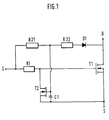
- T1 denotes an n-channel MOSFET power transistor consisting of a plurality of sub-transistors connected in parallel with one another, S denotes its source terminal and D its drain terminal.
- the input terminal G of the MOSFET power transistor T1 is connected to its polysilicon gate via a first ohmic resistor R1.
- An n-channel auxiliary MOSFET transistor T2 is connected with its source electrode to the source electrode of the MOSFET power transistor T1.
- the drain electrode of the auxiliary MOSFET transistor T2 is connected to the polysilicon gate of the power MOSFET transistor T1.
- the polysilicon gate of the auxiliary MOSFET transistor T2 is connected on the one hand via a second ohmic resistor R21 to the input terminal G and on the other hand via the series connection of a third ohmic resistor R22 and a protective diode D1 to the drain terminal D of the MOSFET power transistor T1.
- the polysilicon gate of the auxiliary MOSFET transistor T2 is connected to the one coating of a capacitance C1, the other coating of which is connected to the source electrode of the auxiliary MOSFET transistor T2.
- the mode of operation of the circuit arrangement according to FIG. 1 is as follows:
- the operating voltage is between the drain terminal D and the source terminal S. Since the diode D1 is polarized in the reverse direction, the polysilicon gate of the auxiliary MOSFET transistor T2 and the capacitance C1 are discharged.
- the gate capacitance of the MOSFET power transistor T1 is charged and the gate-source voltage of the MOSFET power transistor T1 (UGS1) increases.
- the gate of the auxiliary MOSFET transistor T2 and the capacitance C1 are charged via the resistor R21. This also increases UGS2. If UGS2 rises above the threshold voltage of the auxiliary MOSFET transistor T2, the switch-on process of the MOSFET power transistor T1 is interrupted and the circuit cannot be switched on. Therefore, the time constant for the rise of UGS2 must be chosen larger than that for the MOSFET power transistor T1.
- a voltage UGS2 is set just below the threshold voltage of the auxiliary MOSFET transistor T2 via the current path G-R21-R22-D1-D. If the current I in the MOSFET power transistor T1 now rises, the voltage drop at the RDS (on) increases and thus the potential of the drain connection D. As a result, the voltage UGS2 increases.
- the threshold voltage of the auxiliary MOSFET transistor T2 is exceeded, the auxiliary transistor T2 is switched on and thus the voltage UGS1 is reduced. This increases the RDS (on) of the MOSFET power transistor T1 and UDS increases. This increases the effect and UGS2 continues to rise. This leads to complete shutdown of the MOSFET power transistor T1. A restart is only possible if the external voltage UGS is lowered in order to discharge the gate capacitance of the auxiliary MOSFET transistor T2 and the capacitor C1. This means that the normal off state is reached again.
- FIG. 2 shows a section through the monolithically integrated circuit arrangement according to FIG. 1.
- a disk-shaped semiconductor body 100 consisting of single-crystalline silicon contains an n - -conducting epitaxial layer 11, which is applied to an n + -conducting substrate 12 consisting of single-crystalline silicon.
- the semiconductor body 100 consisting of the substrate 12 and the epitaxial layer 11 thus has a first main surface 13 on its upper side and a second main surface 14 on its lower side.
- a metallization 15, which forms the drain terminal D of the vertical MOSFET power transistor T1 is applied to the second main surface 14 of the semiconductor body 100.
- the right part of the sectional view in FIG. 2 shows the known structure of the MOSFET power transistor T1 divided into cells, in which the density of the cells can be up to 2.1 million cells per square inch.
- the middle and the left part shows the edge area in which the peripheral circuit elements are housed.
- the cells of the MOSFET power transistor T1 contain p-doped body zones K, which are each formed by the diffusion of a p + -doped small area 1 and a p - -doped larger area la.
- the smaller area 1 has a greater penetration depth than the larger area 1 a.
- ++ -doped source zones 3 are diffused in each case within the highly doped central region such that the lightly doped Edge region la of the body zones K remains free and extends to the first main surface 13 of the semiconductor body 100.
- the conductivity channel 2 is formed in each cell of the MOSFET power transistor T1 in that a part 9 of the polysilicon gate of the said transistor T1 is opposite this edge region.
- the parts 9 of the polysilicon gate of the MOSFET power transistor T1 serve as a mask in the production of the diffusion zones 1, 1a and 3 and are therefore connected to one another within the cell structure of the MOSFET power transistor T1 in a grid-like and thus electrically conductive manner.
- the source zones 3 are each short-circuited to the body zones K by means of a common metallization 16, which extends to the first main surface 13 of the semiconductor body 100 and the individual parts 9 to form this short-circuit in the central region of each body zone K of the polysilicon gate with the interposition of a silicon dioxide layer 17.
- This common metallization 16 forms the source electrode S of the MOSFET power transistor T1.
- An annular trough 4 serving as a protective ring is diffused around the entire cell field of the MOSFET power transistor T1 and forms the edge structure of the MOSFET power transistor T1 in order to receive the reverse voltage between the electrodes S and D.
- the annular trough 4 is p-conductive. Their doping concentration lies between the doping concentration of the highly doped central region 1 and the doping concentration of the lightly doped edge region la of the body zones K. The same also applies to the penetration depth of the annular trough 4. This lies between the penetration depths of the two regions 1 and 1a of the body zones K mentioned.
- Figure 2 shows the annular trough 4 in an area where it is greatly widened compared to the other areas of the trough.
- This widened region of the well 4 serves to accommodate the lateral n-channel auxiliary MOSFET transistor T2. It is formed by the heavily n-doped zones 7 as the source and 8 as the drain and by the polysilicon layer 10 as the gate.
- the n ++ -doped zones 7 and 8 are produced with the same diffusion process as the source zones 3 of the MOSFET power transistor T1.
- the protective ring 4 overlaps in its widened area, the.
- the body zone of the auxiliary MOSFET transistor T2 forms the body zone of the auxiliary MOSFET transistor T2, with the body zone K of the outermost cell of the MOSFET power transistor T1 adjoining it, in such a way that its source zone 7 is completely embedded in said body zone K and that its drain zone 8 is in the region outside said body zone K is located.
- the overlap is furthermore carried out in such a way that the weakly doped edge region la of the aforementioned body zone K of the MOSFET power transistor T1 extends into the channel region of the auxiliary MOSFET transistor T2.
- the threshold voltage of the auxiliary MOSFET transistor T2 is determined by both regions 4 and 1 a and the epitaxial layer 11 and is therefore higher than the threshold voltage of the power MOSFET transistor T1, which is determined only by the diffusion region 1 a and the epitaxial layer 11.
- a further p-conducting zone 5 is diffused into the single-crystalline semiconductor body 100, the pn junction with the epitaxial layer 11 forming the protective diode D1 according to FIG.
- FIG. 3 shows a further exemplary embodiment of a monolithically integrated circuit arrangement according to the invention, in which the annular well 4 also contains, in a widened area, a lateral n-channel auxiliary MOSFET transistor T2, the source zone again with 7 and the drain zone again with 8 and the polysilicon gate thereof is designated by 10.
- the widened area of the protective ring 4 overlaps again with the body zone K of the outermost cell of the MOSFET power transistor T1 adjoining it.
- source zone 7 is only partially embedded in said body zone K of MOSFET power transistor T1.
- the weakly doped edge region la of the aforementioned body zone K does not extend here into the channel region of the auxiliary MOSFET transistor T2 lying under the polysilicon gate 10, but rather already ends in the region of the source zone 7. This ensures that the threshold voltage of the auxiliary MOSFET transistor T2 only is determined by the region 4 and the epitaxial layer 11. In this way, a threshold voltage can be implemented for the auxiliary MOSFET transistor T2 that is lower or greater than the threshold voltage of the power MOSFET transistor T1.
- the capacitance designated C1 in FIG. 1 is realized in that the polysilicon gate 10 belonging to the auxiliary MOSFET transistor T2 overlaps in the region of the protective ring 4 in a manner not shown in FIGS. 2 and 3 extends the channel region of the auxiliary MOSFET transistor T2, for example in a direction perpendicular to the plane of the drawing in FIGS. 2 and 3.
- FIG. 1 A further circuit arrangement according to the invention is shown in FIG. In addition to the circuit elements in FIG. 1, it shows a first zener diode D2 for protecting the gate of the MOSFET power transistor T1 against overvoltages and a second zener diode D3 for protecting the gate of the MOSFET auxiliary transistor T2 against overvoltages, the cathodes of the two zener diodes D2, D3 are each connected to the gate to be protected and their anodes to the source electrode S of the MOSFET power transistor T1 connected to ground.
- FIG. 5 shows how the two Zener diodes D2 and D3 are integrated monolithically.
- the first zener diode D2 is formed by a further zone 13 with the conductivity type of the semiconductor body, but increased impurity concentration, which is diffused into the protective ring 4, the zone 13 forming the cathode of the first zener diode D2 and via the connection line indicated at 18 to the Polysilicon gate 9 of the MOSFET power transistor T1 is connected.
- the second zener diode D3 is formed by a further zone 14 with the conductivity type of the semiconductor body, but increased impurity concentration, which is diffused into the protective ring 4, the zone 14 forming the cathode of the second zener diode D3 and via the connection line indicated at 19 to the Polysilicon gate 10 of the auxiliary MOSFET transistor T2 is connected.
- the protective ring 4 forms the common anode for both Zener diodes D2, D3, the protective ring 4 being connected to ground via the common source metallization 16 of the MOSFET power transistor T1.
- the invention is not limited to the exemplary embodiments described with reference to the drawing.
- further peripheral circuit elements in particular the resistors R1, R21 and R22, can be integrated in the protective ring 4, it being possible for the resistors mentioned to be designed as n ++ -doped diffused resistors.
- these resistors can also consist of polysilicon and can be accommodated in the plane of the polysilicon gates 9 and 10 and can be produced simultaneously with these gates.
- MOSFET power transistor T1 is designed as a so-called SENSEFET, that is to say to provide some of its cells with a separate source connection which has no electrically conductive connection with the common source metallization 16 of the remaining cells.
- connection metallization and / or resistors it is also possible to design and arrange conductor tracks of the connection metallization and / or resistors in such a way that an adjustment of the circuit is possible by deliberately blowing them through.
- the particular advantage of the present monolithically integrated circuit arrangement in comparison with the known discrete circuitry according to the invention is that manufacturing variations affect the individual circuit elements of the integrated circuit in the same way. In this way, extensive “tracking" of the threshold voltages is achieved. Furthermore, the temperature coefficient of the RDS (on) and the resistors R21 and R22 is used in such a way that the overload detection takes place earlier at a high chip temperature than at a low chip temperature. This protects the circuit against excessive operating temperatures.
- all semiconductor regions can also be of the opposite conductivity type, that is to say n and p-type regions can be interchanged. In this way, a short-circuit-proof p-channel MOSFET power transistor according to the invention can be implemented.
Abstract
Description
Die Erfindung betrifft eine monolithisch integrierte Schaltungsanordnung nach der Gattung des Hauptanspruchs.The invention relates to a monolithically integrated circuit arrangement according to the preamble of the main claim.
Es sind bereits MOSFET-Leistungstransistoren bekannt, die aus einer Vielzahl zueinander parallelgeschalteter Teiltransistoren (Zellen) bestehen, die in einem einzigen, einkristallinen, aus Silizium bestehenden Halbleiterkörper untergebracht sind. Die Gesamtheit aller Teiltransistoren kann dabei von einer Diffusionszone umschlossen sein, die als Schutzring um den Zellverband des MOSFET-Leistungstransistors gelegt ist.MOSFET power transistors are already known which consist of a plurality of partial transistors (cells) connected in parallel with one another, which are accommodated in a single, single-crystalline semiconductor body consisting of silicon. The entirety of all partial transistors can be enclosed by a diffusion zone, which is placed as a protective ring around the cell structure of the MOSFET power transistor.
Andererseits sind bereits Schutzschaltungen bekanntgeworden, die zum Schutz der MOSFET-Leistungstransistoren, insbesondere zum Schutz dieser Transistoren gegen Kurzschluß und Überspannungen, dienen. Die die Schutzfunktion übernehmenden aktiven und/oder passiven Schaltungseinheiten sind dabei als diskrete Bauelemente dem MOSFET-Leistungstransistor extern zugeschaltet.On the other hand, protective circuits have already become known which serve to protect the MOSFET power transistors, in particular to protect these transistors against short circuits and overvoltages. The active and / or passive circuit units assuming the protective function are externally connected to the MOSFET power transistor as discrete components.
Das Dokument US-A-4 893 212 offenbart eine Schaltungsanordnung bestehend aus einem vertikalen MOSFET Leistungstransistor, einem bipolaren Transistor und einem Schutzring.Document US-A-4 893 212 discloses a circuit arrangement consisting of a vertical MOSFET power transistor, a bipolar transistor and a guard ring.
Eine monolithisch integrierte Schaltungsanordnung gemäß der Erfindung ist in Anspruch 1 definiert. Weitere Ausführungsformen sind in den Unteransprüchen 2-15 definiert.A monolithically integrated circuit arrangement according to the invention is defined in
Anhand der Zeichnung wird die Erfindung näher erläutert. Es zeigen:
Figur 1 einen MOSFET-Leistungstransistor mit einer Schutzschaltung, die den MOSFET-Leistungstransistor im Falle von Überlast oder Kurzschluß abschaltet, im Schaltbild,- Figur 2 ein Schnittbild durch einen scheibenförmigen einkristallinen Halbleiterkörper aus Silizium, der die Schaltungsanordnung nach
Figur 1 in monolithisch integrierter Form gemäß einem ersten Ausführungsbeispiel der Erfindung enthält, teilweise abgebrochen, Figur 3 ein zweites Ausführungsbeispiel einer erfindungsgemäßen monolithisch integrierten Ausgestaltung der Schaltungsanordnung nachFigur 1, im Schnitt, teilweise abgebrochen,Figur 4 eine Weiterbildung der Schaltungsanordnung nachFigur 1,Figur 5 ein Schnittbild einer monolithisch integrierten Ausgestaltung der Schaltungsanorndung nachFigur 4 als drittes Ausführungsbeispiel einer monolithisch integrierten Schaltungsanordnung gemäß der Erfindung.
- FIG. 1 shows a MOSFET power transistor with a protective circuit, which switches the MOSFET power transistor off in the event of an overload or short circuit, in the circuit diagram,
- 2 shows a sectional view through a disk-shaped single-crystalline semiconductor body made of silicon, which contains the circuit arrangement according to FIG. 1 in a monolithically integrated form according to a first exemplary embodiment of the invention, partially broken off, FIG.
- FIG. 3 shows a second exemplary embodiment of a monolithically integrated embodiment of the circuit arrangement according to FIG. 1, in section, partially broken off,
- FIG. 4 shows a further development of the circuit arrangement according to FIG. 1,
- 5 shows a sectional view of a monolithically integrated configuration of the circuit arrangement according to FIG. 4 as a third exemplary embodiment of a monolithically integrated circuit arrangement according to the invention.
Bei dem in Figur 1 dargestellten Schaltbild ist mit T1 ein aus einer Vielzahl zueinander parallelgeschalteter Teiltransistoren bestehender n-Kanal-MOSFET-Leistungstransistor, mit S seine Sourceanschlußklemme und mit D seine Drainanschlußklemme bezeichnet. Die Eingangsklemme G des MOSFET-Leistungstransistors T1 ist über einen ersten ohmschen Widerstand R1 mit seinem Polysilizium-Gate verbunden.In the circuit diagram shown in FIG. 1, T1 denotes an n-channel MOSFET power transistor consisting of a plurality of sub-transistors connected in parallel with one another, S denotes its source terminal and D its drain terminal. The input terminal G of the MOSFET power transistor T1 is connected to its polysilicon gate via a first ohmic resistor R1.
Ein n-Kanal-MOSFET-Hilfstransistor T2 ist mit seiner Sourceelektrode an die Sourceelektrode des MOSFET-Leistungstransistors T1 angeschlossen. Die Drainelektrode des MOSFET-Hilfstransistors T2 ist an das Polysilizium-Gate des MOSFET-Leistungstransistors T1 angeschlossen. Das Polysilizium-Gate des MOSFET-Hilfstransistors T2 ist einerseits über einen zweiten ohmschen Widerstand R21 mit der Eingangsklemme G und andererseits über die Reihenschaltung eines dritten ohmschen Widerstands R22 und einer Schutzdiode D1 mit der Drainanschlußklemme D des MOSFET-Leistungstransistors T1 verbunden. Des weiteren ist das Polysilizium-Gate des MOSFET-Hilfstransistors T2 mit dem einen Belag einer Kapazität C1 verbunden, deren anderer Belag an die Sourceelektrode des MOSFET-Hilfstransistors T2 angeschlossen ist.An n-channel auxiliary MOSFET transistor T2 is connected with its source electrode to the source electrode of the MOSFET power transistor T1. The drain electrode of the auxiliary MOSFET transistor T2 is connected to the polysilicon gate of the power MOSFET transistor T1. The polysilicon gate of the auxiliary MOSFET transistor T2 is connected on the one hand via a second ohmic resistor R21 to the input terminal G and on the other hand via the series connection of a third ohmic resistor R22 and a protective diode D1 to the drain terminal D of the MOSFET power transistor T1. Furthermore, the polysilicon gate of the auxiliary MOSFET transistor T2 is connected to the one coating of a capacitance C1, the other coating of which is connected to the source electrode of the auxiliary MOSFET transistor T2.
Die Wirkungsweise der Schaltungsanordnung nach Figur 1 ist folgende:The mode of operation of the circuit arrangement according to FIG. 1 is as follows:
Im ausgeschalteten Zustand liegt zwischen der Eingangsklemme G und der Sourceanschlußklemme S die Spannung UGS = 0. Zwischen der Drainanschlußklemme D und der Sourceanschlußklemme S liegt die Betriebsspannung. Da die Diode D1 in Sperrichtung gepolt ist, werden das Polysiliziumgate des MOSFET-Hilfstransistors T2 und die Kapazität C1 entladen. Die Gate-Source-Spannung des MOSFET-Hilfstransistors T2 ist UGS2 = 0.In the switched-off state, the voltage UGS = 0 is between the input terminal G and the source terminal S. The operating voltage is between the drain terminal D and the source terminal S. Since the diode D1 is polarized in the reverse direction, the polysilicon gate of the auxiliary MOSFET transistor T2 and the capacitance C1 are discharged. The gate-source voltage of the auxiliary MOSFET transistor T2 is UGS2 = 0.
Wird die Anordnung eingeschaltet, das heißt UGS wird auf typisch + 5 Volt erhöht, so wird die Gatekapazität des MOSFET-Leistungstransistors T1 aufgeladen und damit steigt die Gate-Source-Spannung des MOSFET-Leistungstransistors T1 (UGS1). Gleichzeitig werden über den Widerstand R21 das Gate des MOSFET-Hilfstransistors T2 und die Kapazität C1 aufgeladen. Damit steigt auch UGS2. Steigt UGS2 über die Schwellspannung des MOSFET-Hilfstransistors T2, so wird der Einschaltvorgang des MOSFET-Leistungstransistors T1 unterbrochen und die Schaltung läßt sich nicht einschalten. Deshalb muß die Zeitkonstante für das Ansteigen von UGS2 größer gewählt werden als die für den MOSFET-Leistungstransistors T1. Unter dieser Bedingung ergibt sich folgender Einschaltvorgang: UGS1 steigt über die Schwellspannung des MOSFET-Leistungstransistors T1 und es fließt über diesen Transistor ein Strom I. Die Spannung UDS ergibt sich in diesem Zustand als UDS = RDS (on) I. Ist dieser Wert klein genug, so wird ein Stromfluß vom Gate des MOSFET-Hilfstransistors T2 über den Widerstand R22 und die Diode D1 zum Drainanschluß D einsetzen und der Ladevorgang des Gates des MOSFET-Hilfstransistors T2 wird abgebrochen. Damit wird der MOSFET-Hilfstransistor T2 nicht eingeschaltet und die gesamte Schaltung ist im Einzustand.If the arrangement is switched on, that is to say UGS is increased to typically + 5 volts, the gate capacitance of the MOSFET power transistor T1 is charged and the gate-source voltage of the MOSFET power transistor T1 (UGS1) increases. At the same time, the gate of the auxiliary MOSFET transistor T2 and the capacitance C1 are charged via the resistor R21. This also increases UGS2. If UGS2 rises above the threshold voltage of the auxiliary MOSFET transistor T2, the switch-on process of the MOSFET power transistor T1 is interrupted and the circuit cannot be switched on. Therefore, the time constant for the rise of UGS2 must be chosen larger than that for the MOSFET power transistor T1. Under this condition, the following switch-on process results: UGS1 rises above the threshold voltage of the MOSFET power transistor T1 and a current I flows through this transistor. The voltage UDS results in this state as UDS = RDS (on) I. If this value is small enough , a current flow from the gate of the auxiliary MOSFET transistor T2 through the resistor R22 and the diode D1 to the drain terminal D will start and the charging of the gate of the auxiliary MOSFET transistor T2 will be terminated. The MOSFET auxiliary transistor T2 is thus not switched on and the entire circuit is in the on state.
Im normalen Einzustand wird über den Strompfad G-R21-R22-D1-D eine Spannung UGS2 knapp unter der Schwellspannung des MOSFET-Hilfstransistors T2 eingestellt. Steigt nun der Strom I im MOSFET-Leistungstransistor T1, so steigt der Spannungsabfall am RDS (on) und damit das Potential des Drainanschlusses D. Als Folge steigt die Spannung UGS2. Beim Überschreiten der Schwellspannung des MOSFET-Hilfstransistors T2 wird der Hilfstransistor T2 eingeschaltet und damit die Spannung UGS1 erniedrigt. Dadurch steigt der RDS (on) des MOSFET-Leistungstransistors T1 und UDS steigt an. Dadurch wird der Effekt verstärkt und UGS2 steigt weiter. Dies führt zur vollständigen Abschaltung des MOSFET-Leistungstransistors T1. Ein Wiedereinschalten ist nur möglich, wenn die externe Spannung UGS erniedrigt wird, um die Gatekapazität des MOSFET-Hilfstransistors T2 und den Kondensator C1 zu entladen. Damit ist der normale Auszustand wieder erreicht.In the normal state, a voltage UGS2 is set just below the threshold voltage of the auxiliary MOSFET transistor T2 via the current path G-R21-R22-D1-D. If the current I in the MOSFET power transistor T1 now rises, the voltage drop at the RDS (on) increases and thus the potential of the drain connection D. As a result, the voltage UGS2 increases. When the threshold voltage of the auxiliary MOSFET transistor T2 is exceeded, the auxiliary transistor T2 is switched on and thus the voltage UGS1 is reduced. This increases the RDS (on) of the MOSFET power transistor T1 and UDS increases. This increases the effect and UGS2 continues to rise. This leads to complete shutdown of the MOSFET power transistor T1. A restart is only possible if the external voltage UGS is lowered in order to discharge the gate capacitance of the auxiliary MOSFET transistor T2 and the capacitor C1. This means that the normal off state is reached again.
In Figur 2 ist ein Schnitt durch die monolithisch integrierte Schaltungsanordnung nach Figur 1 dargestellt. Ein scheibenförmiger, aus einkristallinem Silizium bestehender Halbleiterkörper 100 enthält eine n--leitende Epitaxialschicht 11, die auf ein n+-leitendes, aus einkristallinem Silizium bestehendes Substrat 12 aufgebracht ist. Der aus dem Substrat 12 und der Epitaxialschicht 11 bestehende Halbleiterkörper 100 weist somit an seiner Oberseite eine erste Hauptoberfläche 13 und an seiner Unterseite eine zweite Hauptoberfläche 14 auf. Auf die zweite Hauptoberfläche 14 des Halbleiterkörpers 100 ist eine Metallisierung 15 aufgebracht, die den Drainanschluß D des vertikalen MOSFET-Leistungstransistors T1 bildet.FIG. 2 shows a section through the monolithically integrated circuit arrangement according to FIG. 1. A disk-
Der rechte Teil des Schnittbildes der Figur 2 zeigt den an sich bekannten, in Zellen unterteilten Aufbau des MOSFET-Leistungstransistors T1, bei dem die Dichte der Zellen bis zu 2,1 Millionen Zellen pro Quadratinch betragen kann. Der mittlere und der linke Teil zeigt den Randbereich, in welchem die peripheren Schaltungselemente untergebracht sind.The right part of the sectional view in FIG. 2 shows the known structure of the MOSFET power transistor T1 divided into cells, in which the density of the cells can be up to 2.1 million cells per square inch. The middle and the left part shows the edge area in which the peripheral circuit elements are housed.
Die Zellen des MOSFET-Leistungstransistors T1 enthalten p-dotierte Körperzonen K, die jeweils durch Ineinanderdiffundieren einer p+-dotierten kleinflächigeren Zone 1 und einer p--dotierten großflächigeren Zone la gebildet sind. Die kleinflächigere Zone 1 hat dabei jeweils eine höhere Eindringtiefe als die großflächigere Zone 1a. In die so gebildeten p-dotierten Körperzonen K sind jeweils innerhalb des hochdotierten Zentralbereichsn++-dotierte Sourcezonen 3 derart eindiffundiert, daß der niedrig dotierte Randbereich la der Körperzonen K freibleibt und bis an die erste Hauptoberfläche 13 des Halbleiterkörpers 100 reicht. In diesem Randbereich der Körperzonen K wird der Leitfähigkeitskanal 2 in jeder Zelle des MOSFET-Leistungstransistors T1 dadurch gebildet, daß diesem Randbereich jeweils ein Teil 9 des Polysilizium-Gates des genannten Transistors T1 gegenübersteht. Die Teile 9 des Polysilizium-Gates des MOSFET-Leistungstransistors T1 dienen bei der Herstellung der Diffusionszonen 1, 1a und 3 als Maske und sind deshalb innerhalb des Zellverbandes des MOSFET-Leistungstransistors T1 gitterartig und damit elektrisch leitend miteinander verbunden. Innerhalb jeder Zelle des MOSFET-Leistungstransistors T1 sind die Sourcezonen 3 jeweils mit den Körperzonen K mittels einer gemeinsamen Metallisierung 16 kurzgeschlossen, die zur Bildung dieses Kurzschlusses im Zentralbereich jeder Körperzone K sich bis an die erste Hauptoberfläche 13 des Halbleiterkörpers 100 erstreckt und die einzelnen Teile 9 des Polysiliziumgates unter Zwischenschaltung einer Siliziumdioxidschicht 17 umgreift. Diese gemeinsame Metallisierung 16 bildet die Sourceelektrode S des MOSFET-Leistungstransistors T1.The cells of the MOSFET power transistor T1 contain p-doped body zones K, which are each formed by the diffusion of a p + -doped
Um das gesamte Zellenfeld des MOSFET-Leistungstransistors T1 ist eine als Schutzring dienende ringförmige Wanne 4 eindiffundiert, die die Randstruktur des MOSFET-Leistungstransistors T1 bildet, um die Sperrspannung zwischen den Elektroden S und D aufzunehmen. Die ringförmige Wanne 4 ist p-leitend. Ihre Dotierungskonzentration liegt zwischen der Dotierungskonzentration des hochdotierten Zentralbereichs 1 und der Dotierungskonzentration des niedrig dotierten Randbereichs la der Körperzonen K. Entsprechendes gilt auch für die Eindringtiefe der ringförmigen Wanne 4. Diese liegt zwischen den Eindringtiefen der beiden genannten Bereiche 1 und 1a der Körperzonen K.An
Figur 2 zeigt die ringförmige Wanne 4 in einem Bereich, wo sie gegenüber den übrigen Bereichen der Wanne stark verbreitert ist. Dieser verbreiterte Bereich der Wanne 4 dient zur Aufnahme des lateralen n-Kanal-MOSFET-Hilfstransistors T2. Er wird gebildet von den stark n-dotierten Zonen 7 als Source und 8 als Drain sowie von der Polysiliziumschicht 10 als Gate. Die n++-dotierten Zonen 7 und 8 sind dabei mit dem gleichen Diffusionsprozeß hergestellt wie die Sourcezonen 3 des MOSFET-Leistungstransistors T1. Wie aus Figur 2 ersichtlich, überlappt sich der Schutzring 4 in seinem verbreiterten Bereich, der. die Körperzone des MOSFET-Hilfstransistors T2 bildet, mit der Körperzone K der an ihn angrenzenden äußersten Zelle des MOSFET-Leistungstransistors T1 derart, daß seine Sourcezone 7 vollständig in die genannte Körperzone K eingebettet ist und daß seine Drainzone 8 sich im Bereich außerhalb der genannten Körperzone K befindet. Die Überlappung ist dabei des weiteren so ausgeführt, daß der schwach dotierte Randbereich la der genannten Körperzone K des MOSFET-Leistungstransistors T1 sich bis in den Kanalbereich des MOSFET-Hilfstransistors T2 erstreckt. Dadurch wird erreicht, daß die Schwellspannung des MOSFET-Hilfstransistors T2 von beiden Gebieten 4 und la sowie der Epitaxialschicht 11 bestimmt wird und damit höher ist als die Schwellspannung des MOSFET-Leistungstransistors T1, die nur durch das Diffusionsgebiet la und die Epitaxialschicht 11 bestimmt wird.Figure 2 shows the
Gleichzeitig mit dem Schutzring 4 ist in den einkristallinen Halbleiterkörper 100 eine weitere p-leitende Zone 5 eindiffundiert, deren pn-Übergang mit der Epitaxialschicht 11 die Schutzdiode D1 nach Figur 1 bildet.Simultaneously with the
Figur 3 zeigt ein weiteres Ausführungsbeispiel einer erfindungsgemäßen monolithisch integrierten Schaltungsanordnung, bei dem ebenfalls die ringförmige Wanne 4 in einem verbreiterten Bereich einen lateralen n-Kanal-MOSFET-Hilfstransistor T2 enthält, dessen Sourcezone wieder mit 7 und dessen Drainzone wieder mit 8 und dessen Polysiliziumgate wieder mit 10 bezeichnet ist. Der verbreiterte Bereich des Schutzrings 4 überlappt sich auch hier wieder mit der Körperzone K der an ihn angrenzenden äußersten Zelle des MOSFET-Leistungstransistors T1. Die Sourcezone 7 ist hier jedoch nur teilweise in die genannte Körperzone K des MOSFET-Leistungstransistors T1 eingebettet. Der schwach dotierte Randbereich la der genannten Körperzone K erstreckt sich hier nicht bis in den unter dem Polysiliziumgate 10 liegenden Kanalbereich des MOSFET-Hilfstransistors T2, sondern endet bereits im Bereich der Sourcezone 7. Dadurch wird erreicht, daß die Schwellspannung des MOSFET-Hilfstransistors T2 nur durch das Gebiet 4 und die Epitaxialschicht 11 bestimmt wird. Damit kann für den MOSFET-Hilfstransistor T2 eine Schwellspannung realisiert werden, die kleiner oder größer ist als die Schwellspannung des MOSFET-Leistungstransistors T1.FIG. 3 shows a further exemplary embodiment of a monolithically integrated circuit arrangement according to the invention, in which the
Bei den beiden Ausführungsbeispielen nach den Figuren 2 und 3 wird die in Figur 1 mit C1 bezeichnete Kapazität dadurch realisiert, daß das zum MOSFET-Hilfstransistor T2 gehörende Polysiliziumgate 10 sich im Bereich des Schutzrings 4 in einer in den Figuren 2 und 3 nicht dargestellten Weise über den Kanalbereich des MOSFET-Hilfstransistors T2 hinaus erstreckt, beispielsweise in eine Richtung senkrecht zur Zeichenebene der Figuren 2 und 3.In the two exemplary embodiments according to FIGS. 2 and 3, the capacitance designated C1 in FIG. 1 is realized in that the
In Figur 4 ist eine weitere erfindungsgemäße Schaltungsanordnung dargestellt. Sie zeigt über die Schaltungselemente der Figur 1 hinaus eine erste Zenerdiode D2 zum Schutz des Gates des MOSFET-Leistungstransistors T1 gegen Überspannungen und eine zweite Zenerdiode D3 zum Schutz des Gates des MOSFET-Hilfstransistors T2 gegen Überspannungen, wobei die Kathoden der beiden Zenerdioden D2, D3 jeweils an das zu schützende Gate und ihre Anoden jeweils an die mit Masse verbundene Sourceelektrode S des MOSFET-Leistungstransistors T1 angeschlossen sind.A further circuit arrangement according to the invention is shown in FIG. In addition to the circuit elements in FIG. 1, it shows a first zener diode D2 for protecting the gate of the MOSFET power transistor T1 against overvoltages and a second zener diode D3 for protecting the gate of the MOSFET auxiliary transistor T2 against overvoltages, the cathodes of the two zener diodes D2, D3 are each connected to the gate to be protected and their anodes to the source electrode S of the MOSFET power transistor T1 connected to ground.
In Figur 5 ist dargestellt, wie die beiden Zenerdioden D2 und D3 monolithisch integriert werden. Die erste Zenerdiode D2 wird durch eine weitere Zone 13 mit dem Leitfähigkeitstyp des Halbleiterkörpers, aber erhöhter Störstellenkonzentration, gebildet, die in den Schutzring 4 eindiffundiert ist, wobei die Zone 13 die Kathode der ersten Zenerdiode D2 bildet und über die bei 18 angedeutete Verbindungsleitung mit dem Polysiliziumgate 9 des MOSFET-Leistungstransistors T1 verbunden ist. Die zweite Zenerdiode D3 wird durch eine weitere Zone 14 mit dem Leitfähigkeitstyp des Halbleiterkörpers, aber erhöhter Störstellenkonzentration, gebildet, die in den Schutzring 4 eindiffundiert ist, wobei die Zone 14 die Kathode der zweiten Zenerdiode D3 bildet und über die bei 19 angedeutete Verbindungsleitung mit dem Polysiliziumgate 10 des MOSFET-Hilfstransistors T2 verbunden ist. Der Schutzring 4 bildet für beide Zenerdioden D2, D3 die gemeinsame Anode, wobei der Schutzring 4 über die gemeinsame Sourcemetallisierung 16 des MOSFET-Leistungstransistors T1 mit Masse verbunden ist.FIG. 5 shows how the two Zener diodes D2 and D3 are integrated monolithically. The first zener diode D2 is formed by a
Die Erfindung ist nicht auf die anhand der Zeichnung beschriebenen Ausführungsbeispiele beschränkt. Insbesondere können außer den Schaltungselementen T2, D2 und D3 noch weitere periphere Schaltungselemente, insbesondere die Widerstände R1, R21 und R22 in dem Schutzring 4 integriert sein, wobei die genannten Widerstände als n++-dotierte diffundierte Widerstände ausgeführt sein können. Alternativ dazu können diese Widerstände aber auch aus Polysilizium bestehen und in der Ebene der Polysiliziumgates 9 und 10 untergebracht und gleichzeitig mit diesen Gates hergestellt sein.The invention is not limited to the exemplary embodiments described with reference to the drawing. In particular, in addition to the circuit elements T2, D2 and D3, further peripheral circuit elements, in particular the resistors R1, R21 and R22, can be integrated in the
Im Rahmen der Erfindung liegt es auch, den MOSFET-Leistungstransistor T1 als sogenannten SENSEFET auszubilden, das heißt, einige seiner Zellen mit einem separaten Sourceanschluß zu versehen, der mit der gemeinsamen Sourcemetallisierung 16 der verbleibenden Zellen keine elektrisch leitende Verbindung hat.It is also within the scope of the invention to design the MOSFET power transistor T1 as a so-called SENSEFET, that is to say to provide some of its cells with a separate source connection which has no electrically conductive connection with the
Auch ist es möglich, Leiterbahnen der Verbindungsmetallisierung und/oder Widerstände so auszubilden und anzuordnen, daß durch deren gezieltes Durchbrennen ein Abgleich der Schaltung möglich ist.It is also possible to design and arrange conductor tracks of the connection metallization and / or resistors in such a way that an adjustment of the circuit is possible by deliberately blowing them through.
Der besondere Vorteil der vorliegenden monolithisch integrierten Schaltungsanordnung besteht im Vergleich zu der bekannten diskreten Beschaltung erfindungsgemäß darin, daß Fertigungsstreuungen sich auf die einzelnen Schaltungselemente der integrierten Schaltung in gleicher Weise auswirken. So wird ein weitgehendes "Tracking" der Schwellspannungen erreicht. Weiterhin wird der Temperaturkoeffizient des RDS (on) und der Widerstände R21 und R22 in der Weise ausgenützt, daß die Überlasterkennung bei hoher Chiptemperatur früher erfolgt als bei tiefer Chiptemperatur. Dadurch wird ein Schutz der Schaltung vor zu hohen Betriebstemperaturen erreicht.The particular advantage of the present monolithically integrated circuit arrangement in comparison with the known discrete circuitry according to the invention is that manufacturing variations affect the individual circuit elements of the integrated circuit in the same way. In this way, extensive "tracking" of the threshold voltages is achieved. Furthermore, the temperature coefficient of the RDS (on) and the resistors R21 and R22 is used in such a way that the overload detection takes place earlier at a high chip temperature than at a low chip temperature. This protects the circuit against excessive operating temperatures.
Im Unterschied zu den anhand der Zeichnung beschriebenen Ausführungsbeispielen können alle Halbleitergebiete auch vom entgegengesetzten Leitfähigkeitstyp sein, das heißt n- und p-leitende Gebiete können vertauscht sein. Auf diese Weise kann ein erfindungsgemäßer kurzschlußfester p-Kanal-MOSFET-Leistungstransistor realisiert werden.In contrast to the exemplary embodiments described with reference to the drawing, all semiconductor regions can also be of the opposite conductivity type, that is to say n and p-type regions can be interchanged. In this way, a short-circuit-proof p-channel MOSFET power transistor according to the invention can be implemented.
Claims (15)
- Monolithically integrated circuit arrangement, 1 which is accommodated in a monocrystalline semiconductor body (100) of a first conductivity type, which semiconductor body is composed of silicon, is in the form of a wafer and has a first and a second main surface, having a vertical MOSFET power transistor (T1), in which the drain zone extends from the first to the second main surface and is provided with a continuous drain terminal (D) on the second main surface, in which at least one body zone (K) of a second conductivity type opposite to that of the semiconductor body is diffused into the semiconductor body (100) from the first main surface (13), in which in each case at least one source zone (3) having the conductivity type of the semiconductor body but an increased impurity concentration is diffused into the at least one body zone (K) from the first main surface (13), and in which there is provided at least one polysilicon gate (9) for forming the conductivity channel (2), and having a protective ring (4) which encloses the MOSFET power transistor (T1) and has the conductivity type of the at least one body zone (K), further zones (7, 8; 13; 14) for forming at least one peripheral circuit element (T2; D2; D3; R1; R21; R22) being diffused into the protective ring (4) from the first main surface (13), characterized in that at least one lateral MOSFET auxiliary transistor (T2) is provided as the peripheral circuit element, the protective ring (4) serving as body zone for the lateral MOSFET auxiliary transistor (T2), furthermore the source zone (7) and the drain zone (8) of the MOSFET auxiliary transistor (T2) having the same doping of the first conductivity type as the at least one source zone (3) of the MOSFET power transistor (T1) and being formed adjacent to one another in the protective ring (4), and the gate electrode (10) of the MOSFET auxiliary transistor (T2) extending over that region of the protective ring (4) which lies between the source zone (7) and drain zone (8) and in which, during operation, the conductivity channel (20) of the MOSFET auxiliary transistor (T2) is formed at the first main surface (13) of the semiconductor body (100).
- Circuit arrangement according to Claim 1, characterized in that the body zone (K) of the MOSFET power transistor (T1) is formed by a smaller-area zone (1) and a larger-area zone (la), the smaller-area zone (1) having a higher doping concentration than the protective zone (4) and the larger-area zone (la) having a lower doping concentration than the protective zone (4), and the two abovementioned different-area zones (1, la), which are superposed to form the body zone (K), being diffused into one another in such a way that the larger-area zone (la) projects over the smaller-area zone (1) on all sides.
- Circuit arrangement according to Claim 1 or 2, characterized in that the MOSFET power transistor (T1) consists of a multiplicity of transistor elements which are connected in parallel with one another and each of which has a body zone (K) and at least one source zone (3), but all of the transistor elements have a common drain zone which is formed by the remaining region of the semiconductor body (100), which region is not occupied by the body zones (K) and is delimited by the protective ring (4).
- Circuit arrangement according to Claim 1, characterized in that, in that region in which it accommodates the MOSFET auxiliary transistor (T2), the protective ring (4) overlaps the body zone (K) of the outermost cell, adjoining the said transistor, of the MOSFET power transistor (T1).
- Circuit arrangement according to Claim 4, characterized in that the source zone (7) of the MOSFET auxiliary transistor (T2) is completely embedded in the body zone (K) of the outermost cell, adjoining the said transistor, of the MOSFET power transistor (T1), and in that the drain zone (8) of the MOSFET auxiliary transistor (T2) is situated in the region outside this body zone (K), with the result that the edge region (la) of the said body zone (K) of the MOSFET power transistor (T1) extends right into the channel region of the MOSFET auxiliary transistor (T2).
- Circuit arrangement according to Claim 4, characterized in that the source zone (7) of the MOSFET auxiliary transistor (T2) is partially embedded in the body zone (K), overlapping the protective ring (4), of the outermost cell, adjoining the said transistor, of the MOSFET power transistor (T1).
- Circuit arrangement according to Claim 5 or 6, characterized in that the source zone (7) of the MOSFET auxiliary transistor (T2) is short-circuited with the source zone (3) of the outermost cell, adjoining the said transistor, of the MOSFET power transistor (T1) and with the protective ring (4) by means of the source metallization layer (S) of the MOSFET power transistor (T1).
- Circuit arrangement according to Claim 7, characterized in that the drain electrode of the MOSFET auxiliary transistor (T2) is connected, on the one hand, directly to the gate electrode of the MOSFET power transistor (T1) and, on the other hand, via a first non-reactive resistor (R1) to the input terminal (G) of the MOSFET power transistor (T1), in that the gate electrode of the MOSFET auxiliary transistor (T2) is connected, on the one hand, via a second non-reactive resistor (R21) to the said input terminal (G) and, on the other hand, via a protective diode (D1) to the drain electrode (D) of the MOSFET power transistor (T1), in that the first electrode of the protective diode (D1) is formed by the semiconductor body in the form of a wafer and the second electrode of the protective diode (D1) is formed by a further zone (5) having the opposite conductivity type to that of the semiconductor body (100), which further zone is diffused into the semiconductor body (100) from the first main surface.
- Circuit arrangement according to Claim 8, characterized in that the zone (5) forming the second electrode of the protective diode (D1) has the same doping of the second conductivity type as the zone forming the protective ring (4) .
- Circuit arrangement according to Claim 8 or 9, characterized in that a first zener diode (D2) is provided for protecting the gate of the MOSFET power transistor (T1) against overvoltages, in that, in order to form the first zener diode (D2), a further zone (13) having the conductivity type of the semiconductor body but an increased impurity concentration is diffused into the protective ring (4), the further zone (13) forming one electrode and the protective ring (4) forming the other electrode of the first zener diode (D2).
- Circuit arrangement according to one of Claims 8 to 10, characterized in that a second zener diode (D3) is provided for protecting the gate of the MOSFET auxiliary transistor (T2) against overvoltages, in that, in order to form the second zener diode (D3), a further zone (14) having the conductivity type of the semiconductor body but an increased impurity concentration is diffused into the protective ring (4), and in that the further zone (14) forms one electrode and the protective ring (4) the other electrode of the second zener diode (D3).
- Circuit arrangement according to Claim 1, characterized in that the MOSFET power transistor (T1) is designed as a SENSEFET power transistor in that at least one of its transistor elements is provided with a separate source terminal.
- Circuit arrangement according to one of Claims 1 to 12, characterized in that at least one non-reactive resistor (R1, R21, R22) is accommodated as a diffused resistor in the protective ring (4) and has the conductivity type of the semiconductor body (100) but an increased impurity concentration.
- Circuit arrangement according to one of Claims 1 to 13, characterized in that at least one non-reactive resistor (R1, R21, R22) consists of polysilicon and is accommodated in the plane of the polysilicon gate (9) of the MOSFET power transistor (T1).
- Circuit arrangement according to one of Claims 1 to 14, characterized by at least one capacitor (C1), one plate (10) of which consists of polysilicon and is accommodated in the plane of the polysilicon gate (9) of the MOSFET power transistor (T1), and the other plate of which is formed at least partially by the protective ring (4).
Applications Claiming Priority (3)
| Application Number | Priority Date | Filing Date | Title |
|---|---|---|---|
| DE4120394A DE4120394A1 (en) | 1991-06-20 | 1991-06-20 | MONOLITHICALLY INTEGRATED CIRCUIT ARRANGEMENT |
| DE4120394 | 1991-06-20 | ||
| PCT/DE1992/000479 WO1993000709A1 (en) | 1991-06-20 | 1992-06-10 | Monolithically integrated circuit |
Publications (2)
| Publication Number | Publication Date |
|---|---|
| EP0591476A1 EP0591476A1 (en) | 1994-04-13 |
| EP0591476B1 true EP0591476B1 (en) | 1996-12-18 |
Family
ID=6434387
Family Applications (1)
| Application Number | Title | Priority Date | Filing Date |
|---|---|---|---|
| EP93901021A Expired - Lifetime EP0591476B1 (en) | 1991-06-20 | 1992-06-10 | Monolithically integrated circuit |
Country Status (6)
| Country | Link |
|---|---|
| US (1) | US5432371A (en) |
| EP (1) | EP0591476B1 (en) |
| JP (1) | JPH06508958A (en) |
| DE (2) | DE4120394A1 (en) |
| ES (1) | ES2095628T3 (en) |
| WO (1) | WO1993000709A1 (en) |
Families Citing this family (21)
| Publication number | Priority date | Publication date | Assignee | Title |
|---|---|---|---|---|
| JP3168763B2 (en) * | 1992-03-30 | 2001-05-21 | 株式会社デンソー | Semiconductor device and manufacturing method thereof |
| US5372955A (en) * | 1993-08-02 | 1994-12-13 | United Microelectronics Corporation | Method of making a device with protection from short circuits between P and N wells |
| US5510747A (en) * | 1993-11-30 | 1996-04-23 | Siliconix Incorporated | Gate drive technique for a bidirectional blocking lateral MOSFET |
| EP0704889A3 (en) * | 1994-09-29 | 1998-10-21 | Siemens Aktiengesellschaft | Power semiconductors with monolithically integrated test resistor and its fabrication |
| JP3485655B2 (en) * | 1994-12-14 | 2004-01-13 | 株式会社ルネサステクノロジ | Composite MOSFET |
| DE19581809B4 (en) * | 1995-04-06 | 2008-12-24 | Transpacific Ip, Ltd. | MOS cell, multiple cell transistor and IC chip |
| US5602046A (en) * | 1996-04-12 | 1997-02-11 | National Semiconductor Corporation | Integrated zener diode protection structures and fabrication methods for DMOS power devices |
| DE59709662D1 (en) * | 1996-05-21 | 2003-05-08 | Infineon Technologies Ag | MOSFET with temperature protection |
| EP0936674B1 (en) * | 1998-02-10 | 2006-04-26 | STMicroelectronics S.r.l. | Integrated circuit comprising a VDMOS transistor protected against overvoltages between source and gate |
| DE19823768A1 (en) * | 1998-05-28 | 1999-12-02 | Bosch Gmbh Robert | Smart power component |
| US6804100B2 (en) | 1999-12-31 | 2004-10-12 | Nokia Mobile Phones, Ltd. | Method and apparatus for protection of batteries |
| JP2001274402A (en) * | 2000-03-24 | 2001-10-05 | Toshiba Corp | Power semiconductor device |
| CN100421182C (en) * | 2003-02-26 | 2008-09-24 | 旺宏电子股份有限公司 | Electrostatic discharge protective device and method for high voltage input bed |
| JP2005043672A (en) * | 2003-07-22 | 2005-02-17 | Toshiba Matsushita Display Technology Co Ltd | Array substrate and its manufacturing method |
| US20070290261A1 (en) * | 2006-06-15 | 2007-12-20 | System General Corp. | Self-driven ldmos transistor |
| DE102006047244B4 (en) * | 2006-10-04 | 2018-01-18 | Infineon Technologies Austria Ag | Semiconductor device with a monocrystalline semiconductor body and method for producing the same |
| JP2010118548A (en) | 2008-11-13 | 2010-05-27 | Mitsubishi Electric Corp | Semiconductor device |
| JP5367396B2 (en) * | 2009-02-06 | 2013-12-11 | ラピスセミコンダクタ株式会社 | Semiconductor device |
| WO2010125661A1 (en) * | 2009-04-30 | 2010-11-04 | 三菱電機株式会社 | Semiconductor device and method for manufacturing the same |
| JP6641161B2 (en) * | 2015-11-18 | 2020-02-05 | 株式会社 日立パワーデバイス | Semiconductor device and alternator using the same |
| US11417644B2 (en) | 2020-06-17 | 2022-08-16 | Macom Technology Solutions Holdings, Inc. | Integration of multiple discrete GaN devices |
Family Cites Families (6)
| Publication number | Priority date | Publication date | Assignee | Title |
|---|---|---|---|---|
| US4313768A (en) * | 1978-04-06 | 1982-02-02 | Harris Corporation | Method of fabricating improved radiation hardened self-aligned CMOS having Si doped Al field gate |
| IT1213411B (en) * | 1986-12-17 | 1989-12-20 | Sgs Microelettronica Spa | POWER MOS STRUCTURE WITH PROTECTION DEVICE AGAINST OVERVOLTAGE AND PROCESS FOR LASUA MANUFACTURE. |
| US4990976A (en) * | 1987-11-24 | 1991-02-05 | Nec Corporation | Semiconductor device including a field effect transistor having a protective diode between source and drain thereof |
| US4893212A (en) * | 1988-12-20 | 1990-01-09 | North American Philips Corp. | Protection of power integrated circuits against load voltage surges |
| US5023692A (en) * | 1989-12-07 | 1991-06-11 | Harris Semiconductor Patents, Inc. | Power MOSFET transistor circuit |
| JP2633746B2 (en) * | 1991-05-27 | 1997-07-23 | 株式会社東芝 | Semiconductor device |
-
1991
- 1991-06-20 DE DE4120394A patent/DE4120394A1/en not_active Withdrawn
-
1992
- 1992-06-10 WO PCT/DE1992/000479 patent/WO1993000709A1/en active IP Right Grant
- 1992-06-10 DE DE59207732T patent/DE59207732D1/en not_active Expired - Fee Related
- 1992-06-10 JP JP4510107A patent/JPH06508958A/en active Pending
- 1992-06-10 ES ES93901021T patent/ES2095628T3/en not_active Expired - Lifetime
- 1992-06-10 US US08/167,839 patent/US5432371A/en not_active Expired - Fee Related
- 1992-06-10 EP EP93901021A patent/EP0591476B1/en not_active Expired - Lifetime
Also Published As
| Publication number | Publication date |
|---|---|
| JPH06508958A (en) | 1994-10-06 |
| DE4120394A1 (en) | 1992-12-24 |
| ES2095628T3 (en) | 1997-02-16 |
| EP0591476A1 (en) | 1994-04-13 |
| US5432371A (en) | 1995-07-11 |
| DE59207732D1 (en) | 1997-01-30 |
| WO1993000709A1 (en) | 1993-01-07 |
Similar Documents
| Publication | Publication Date | Title |
|---|---|---|
| EP0591476B1 (en) | Monolithically integrated circuit | |
| EP1175700B1 (en) | Semiconductor component | |
| DE19964481B4 (en) | Protective MOS semiconductor device using Zener diodes | |
| DE602004009986T2 (en) | Efficient protective structure against electrostatic reverse discharge between two contact surfaces | |
| DE10302628B4 (en) | Power semiconductor device | |
| DE19651247C2 (en) | Input / output protection circuit | |
| DE69834315T2 (en) | Integrated circuit with a VDMOS transistor, which is protected against overvoltages between source and gate | |
| DE10322593A1 (en) | Semiconductor component with high resistance to effects of electrostatic discharge, includes vertical transient attenuator connected to source or drain of MOSFET | |
| DE2505573C3 (en) | Semiconductor circuit arrangement with two insulating-layer field effect transistors | |
| DE102012111910B4 (en) | A semiconductor device comprising a first and a second semiconductor element | |
| DE19654163B4 (en) | Protection device for a semiconductor circuit | |
| DE10216015A1 (en) | Overvoltage protection circuit for CMOS circuits has potential divider and inverter circuits and switching element formed on same substrate as protected integrated CMOS circuit | |
| DE4022022C2 (en) | Vertical semiconductor device with Zener diode as overvoltage protection | |
| EP1284019B1 (en) | Semiconductor power component | |
| EP0017980B1 (en) | Thyristor controlled by a field-effect transistor | |
| EP0174473A1 (en) | Monolithic integrated power output stage | |
| EP1212796B1 (en) | Esd protective arrangement for signal inputs and outputs, said arrangement having an overvoltage tolerance | |
| EP0656659B1 (en) | ESD protection structure for integrated circuits | |
| DE10123818B4 (en) | Arrangement with protective function for a semiconductor component | |
| DE69834451T2 (en) | Protection device for an integrated MOS transistor sufficient voltage gradient | |
| WO2000042658A1 (en) | Esd protective transistor | |
| DE4429903B4 (en) | Power semiconductor arrangement with overload protection circuit | |
| DE4024728A1 (en) | MOS device, esp. power vertical-MOSFET - with high switch=off capacitance and no signal conductor effects | |
| DE19502731C2 (en) | Circuit arrangement for reverse polarity protection in integrated circuits | |
| DE3626858A1 (en) | PROTECTIVE STRUCTURE FOR INTEGRATED CIRCUITS |
Legal Events
| Date | Code | Title | Description |
|---|---|---|---|
| PUAI | Public reference made under article 153(3) epc to a published international application that has entered the european phase |
Free format text: ORIGINAL CODE: 0009012 |
|
| 17P | Request for examination filed |
Effective date: 19931110 |
|
| AK | Designated contracting states |
Kind code of ref document: A1 Designated state(s): DE ES FR GB IT |
|
| GRAG | Despatch of communication of intention to grant |
Free format text: ORIGINAL CODE: EPIDOS AGRA |
|
| GRAH | Despatch of communication of intention to grant a patent |
Free format text: ORIGINAL CODE: EPIDOS IGRA |
|
| 17Q | First examination report despatched |
Effective date: 19960523 |
|
| GRAH | Despatch of communication of intention to grant a patent |
Free format text: ORIGINAL CODE: EPIDOS IGRA |
|
| GRAA | (expected) grant |
Free format text: ORIGINAL CODE: 0009210 |
|
| AK | Designated contracting states |
Kind code of ref document: B1 Designated state(s): DE ES FR GB IT |
|
| ET | Fr: translation filed | ||
| REF | Corresponds to: |
Ref document number: 59207732 Country of ref document: DE Date of ref document: 19970130 |
|
| REG | Reference to a national code |
Ref country code: ES Ref legal event code: FG2A Ref document number: 2095628 Country of ref document: ES Kind code of ref document: T3 |
|
| ITF | It: translation for a ep patent filed |
Owner name: 0403;07MIFSTUDIO JAUMANN |
|
| GBT | Gb: translation of ep patent filed (gb section 77(6)(a)/1977) |
Effective date: 19970226 |
|
| PLBE | No opposition filed within time limit |
Free format text: ORIGINAL CODE: 0009261 |
|
| STAA | Information on the status of an ep patent application or granted ep patent |
Free format text: STATUS: NO OPPOSITION FILED WITHIN TIME LIMIT |
|
| 26N | No opposition filed | ||
| REG | Reference to a national code |
Ref country code: GB Ref legal event code: IF02 |
|
| PGFP | Annual fee paid to national office [announced via postgrant information from national office to epo] |
Ref country code: GB Payment date: 20020527 Year of fee payment: 11 |
|
| PGFP | Annual fee paid to national office [announced via postgrant information from national office to epo] |
Ref country code: FR Payment date: 20020622 Year of fee payment: 11 |
|
| PGFP | Annual fee paid to national office [announced via postgrant information from national office to epo] |
Ref country code: ES Payment date: 20020626 Year of fee payment: 11 |
|
| PG25 | Lapsed in a contracting state [announced via postgrant information from national office to epo] |
Ref country code: GB Free format text: LAPSE BECAUSE OF NON-PAYMENT OF DUE FEES Effective date: 20030610 |
|
| PG25 | Lapsed in a contracting state [announced via postgrant information from national office to epo] |
Ref country code: ES Free format text: LAPSE BECAUSE OF NON-PAYMENT OF DUE FEES Effective date: 20030611 |
|
| GBPC | Gb: european patent ceased through non-payment of renewal fee |
Effective date: 20030610 |
|
| PG25 | Lapsed in a contracting state [announced via postgrant information from national office to epo] |
Ref country code: FR Free format text: LAPSE BECAUSE OF NON-PAYMENT OF DUE FEES Effective date: 20040227 |
|
| REG | Reference to a national code |
Ref country code: FR Ref legal event code: ST |
|
| REG | Reference to a national code |
Ref country code: ES Ref legal event code: FD2A Effective date: 20030611 |
|
| PG25 | Lapsed in a contracting state [announced via postgrant information from national office to epo] |
Ref country code: IT Free format text: LAPSE BECAUSE OF NON-PAYMENT OF DUE FEES;WARNING: LAPSES OF ITALIAN PATENTS WITH EFFECTIVE DATE BEFORE 2007 MAY HAVE OCCURRED AT ANY TIME BEFORE 2007. THE CORRECT EFFECTIVE DATE MAY BE DIFFERENT FROM THE ONE RECORDED. Effective date: 20050610 |
|
| PGFP | Annual fee paid to national office [announced via postgrant information from national office to epo] |
Ref country code: DE Payment date: 20090825 Year of fee payment: 18 |
|
| PG25 | Lapsed in a contracting state [announced via postgrant information from national office to epo] |
Ref country code: DE Free format text: LAPSE BECAUSE OF NON-PAYMENT OF DUE FEES Effective date: 20110101 |