EP0777294B1 - A radiation shielding device - Google Patents
A radiation shielding device Download PDFInfo
- Publication number
- EP0777294B1 EP0777294B1 EP96308636A EP96308636A EP0777294B1 EP 0777294 B1 EP0777294 B1 EP 0777294B1 EP 96308636 A EP96308636 A EP 96308636A EP 96308636 A EP96308636 A EP 96308636A EP 0777294 B1 EP0777294 B1 EP 0777294B1
- Authority
- EP
- European Patent Office
- Prior art keywords
- antenna
- antennas
- antenna assembly
- elements
- sheet
- Prior art date
- Legal status (The legal status is an assumption and is not a legal conclusion. Google has not performed a legal analysis and makes no representation as to the accuracy of the status listed.)
- Expired - Lifetime
Links
Images



Classifications
-
- H—ELECTRICITY
- H01—ELECTRIC ELEMENTS
- H01Q—ANTENNAS, i.e. RADIO AERIALS
- H01Q1/00—Details of, or arrangements associated with, antennas
- H01Q1/52—Means for reducing coupling between antennas; Means for reducing coupling between an antenna and another structure
- H01Q1/526—Electromagnetic shields
Definitions
- This invention relates to a radiation shielding device and in particular relates to radiation control means for antennas.
- Antennas for use in telecommunications operate at many different frequencies. Transmit and receive wavebands may be separated so that interference between the signals is reduced, as in GSM and other systems. Intermodulation products may, however, still result, and transmit and receive signals may interfere between themselves. Intermodulation products in receive band signals are particularly undesirable; the operating capacity is reduced and/or the callers cannot clearly communicate, whilst operators face lost calls and accordingly a reduction in revenue.
- layered antenna an antenna having ground planes, feed networks and dielectric spacers arranged in layers
- a radiating element including a pair of closely spaced correspondingly apertured ground planes with an interposed printed film circuit, electrically isolated from the ground planes, the film circuit providing excitation elements or probes within the areas of the apertures, to form dipoles, and a feed network for the dipoles.
- there is a linear arrangement of a plurality of such aperture/element configurations are spaced at regular intervals co-linearly in the overall layered/triplate structure to form a linear array.
- spurious signals are emitted from mounting apertures and other surface features associated with the reflector plane, for instance, mounting bolts which couple some of the radiated energy, and coaxial cable connector ports.
- the coaxial cable and/or the cable termination assembly may also radiate spurious signals.
- the effect of all these unwanted signals is that they will couple with other radiating elements to form intermodulation products.
- these intermodulation signals can severely impair the received signal quality, since they will be of a power level comparable to the received signal strength.
- the output power In a transmit mode the output power will be reduced to a certain extent and these intermodulation products can affect the beamshape in an indeterminable fashion.
- US Patent 4386354 describes a method of reducing electromagnetic re-radiation of harmonic and intermodulation products. The method comprises applying a layer of non-water soluble substance.
- EP 0667649 A1 describes a layered antenna having a linear array of radiating elements.
- the invention provides an antenna assembly as defined in claim 1.
- an antenna assembly comprising a support frame and individually mounted antenna elements, wherein a flexible insulator-conductor sheet is interposed between the antenna elements and the support frame. Radiation emitted rearwardly from each antenna is thus prevented whereby the generation of intermodulation products is substantially eliminated.
- the antenna can receive signals which are not degraded by the presence of such intermodulation products due to radiation reflected from emissions radiated rearwardly of the antennas and each individually mounted antenna element operates independently.
- the use of metallised plastics is preferred since it is both low cost and simple. Apertures for coaxial cables and mounting bolts are required in the sheeting but, if not unduly large, will not compromise the effect of the sheilding.
- a method of constructing an antenna arrangement wherein, in the assembly of an antenna comprising a frame and a number of layered antenna elements, a flexible insulator-conductor sheet is inserted between the layered antenna elements and the frame, with apertures being defined therein to aid connection of coaxial feeder cables and attachment of the radiating elements with connecting means.
- a method of receiving and transmitting radio signals in a cellular arrangement including an antenna assembly comprising a support frame and individually mounted layered antenna elements, wherein a flexible insulator-conductor sheet is interposed between the antenna elements and the support frame, wherein the method comprises, in a transmission mode, the steps of feeding signals from transmit electronics to the antenna elements via feeder cables and, in a receive mode, the steps of receiving signals via the antenna elements and feeder cables to receive electronics wherein radiative coupling effects from one antenna element coupling with another antenna element due to radiation emitted from the back plane and feeder cables are minimised.
- the layered antenna element shown in Figure 1 comprises a first metallic ground plane 10 having a pair of identical rectangular apertures 11, a second metallic ground plane 12 and an insulating substrate 13 which is positioned between the two ground planes.
- a metallic conductor pattern which consists of a pair of radiating probes 14, 16 and a common feed network 22a.
- a feed point 24 is provided for connection to an external feed (not shown).
- the feed network 21 is positioned so as to form a microstrip transmission line with portions of the ground planes defining the rectangular apertures. The position of the feed point 24 is chosen so that when an r.f.
- the relative lengths of the two portions of the network 21 are such as to cause the pair of probes 14 and 16 to be fed in anti-phase, thereby creating a dipole antenna radiating element structure.
- the dimensions of the rectangular apertures and the bounding portions of the ground plane are chosen so that the bounding portions 28 parallel with the probes 14, 16 act as parasitic antenna radiating elements, which together with the pair of radiating probes 14, 16 shape the radiation pattern of the antenna.
- ground planes are spaced from the plane of the feed network by dielectric spacing means (not shown) so that the feed network is equally spaced from both ground planes. Spacing between the network and the ground planes can be determined by foamed dielectric sheets or dielectric studs interposed between the various layers. Alternative mechanical means for maintaining the separation of the feed conductor network may be employed, especially if the feed network is supported on a rigid dielectric.
- a layered antenna constructed from a first apertured metal or ground plane 10, a second like metal or ground plane 12 and an interposed film circuit 13.
- the planes 10 and 12 are thin metal sheets, e.g. of aluminium and have substantially identical arrays of apertures 11 formed therein by, for example, press punching.
- the apertures are rectangular and can be formed as part of a single linear array.
- the film circuit 13 comprises a printed copper circuit pattern 14a on a thin dielectric film 14b. When sandwiched between the apertured ground planes part of the copper pattern 14a provides probes 14, 16 which extend into the areas of the apertures. The probes are electrically connected to a common feed point by the remainder of the printed circuit pattern 14a which forms a feed conductor network in a conventional manner.
- the film circuit 13 is located between and spaced from the ground plane by sheets of foamed dielectric material 22.
- the antenna can be deliberately shaped about an axis parallel with the linear array of apertures.
- the triplate structure is creased along an axis 20 substantially co-linear with the linear arrangement of probes 14, 16.
- the two flat portions 24, 26 of the structure on either side of the crease together define an angle ⁇ .
- the beamwidth and shape of the radiation pattern of the antenna in azimuth are controlled by the angle ⁇ in conjunction with the transverse dimension x of the apertures.
- the angle ⁇ defined by the rear face of the triplate structure may be greater or lesser than 180°.
- a flat, unapertured ground plane 28 e.g. a metal plate, situated at a distance behind the array to provide a degree of directionality for the antenna, in order that signals are reflected.
- the antenna elements as shown in the above examples are typically mounted upon a frame.
- Metallic fasteners, apertures and protrusions present on the antenna arrays and ground frames couple with the input signals and radiate at a resonating frequency.
- These resonant frequency signals couple with the operating frequencies to form intermodulation products, which, as discussed earlier are detrimental to the overall performance of the antenna. Similar coupling occurs with "conventional" horn antennas and triplate antennas.
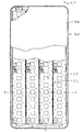
- FIG 4 shows a facet 40 of an antenna made in accordance with the invention.
- the facet comprises four linear arrays 42 arranged in a parallel spaced apart relationship, with a radome 44 (shown part cut-away ).
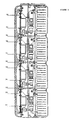
- the antenna arrays are mounted upon a frame 52 as best seen in Figures 5 and 6 by means of electrically insulating fasteners, with flexible metallised plastics film placed between the antenna arrays and the support frame.
- the support frame will be a metal structure and of sufficient strength to support antenna arrays which may be subject to inclement weather conditions.
- the utilisation of flexible metallised film can be easily and simply implemented: a single, wide portion of film may be applied to the frame prior to the attachment of the antennas or individual strips of film may be employed for each linear antenna array.
- the flexible metallised plastics film preferably comprises a layer of metal faced with a layer of plastic on each side.
- the 3M Corporation produce such a type of product, which is known as: 1900 Series Static Shielding Film. It is possible to create a similar effect with the use of a rubber sheet - wire mesh - rubber sheet arrangement. Other combinations of flexible insulating layer - metallic layer sheeting and of flexible insulating layer - metallic layer - insulating layer are possible.
- One feature of the use of metallised plastics film is that it is non-self supporting.
- radio signals are fed to the antenna feed network by, for example, input/output feeds 58 from a base station controller, via amplifiers.
- the feed network divides so that feed probes may radiate within areas defined by apertures in a ground plane of each antenna array.
- Film 54 effectively contains the radiation emanating rearwardly of the antenna arrays 56 due to coupling with the ground planes of the antennas and fasteners 57; microwave input/output feeds 58 are required to pass through this film to couple with feed ports 59 on the rear face of each antenna element, and apertures may be formed or cut in the film to allow coupling of the input/output ports.
- Signal loss by way of radiation leaking through gaps and apertures and through reactive coupling effects is effectively prevented by the flexible metallised film. Spurious signals arising from such connections have been found to be insignificant.
Landscapes
- Physics & Mathematics (AREA)
- Electromagnetism (AREA)
- Variable-Direction Aerials And Aerial Arrays (AREA)
Description
- This invention relates to a radiation shielding device and in particular relates to radiation control means for antennas.
- Antennas for use in telecommunications operate at many different frequencies. Transmit and receive wavebands may be separated so that interference between the signals is reduced, as in GSM and other systems. Intermodulation products may, however, still result, and transmit and receive signals may interfere between themselves. Intermodulation products in receive band signals are particularly undesirable; the operating capacity is reduced and/or the callers cannot clearly communicate, whilst operators face lost calls and accordingly a reduction in revenue.
- One form of layered antenna (an antenna having ground planes, feed networks and dielectric spacers arranged in layers) is known from British application GB-2261554 A (Northern Telecom) and comprises a radiating element including a pair of closely spaced correspondingly apertured ground planes with an interposed printed film circuit, electrically isolated from the ground planes, the film circuit providing excitation elements or probes within the areas of the apertures, to form dipoles, and a feed network for the dipoles. Typically, there is a linear arrangement of a plurality of such aperture/element configurations are spaced at regular intervals co-linearly in the overall layered/triplate structure to form a linear array. This type of antenna lends itself to a cheap yet effective construction for a linear array antenna such as may be utilised for a cellular telephone base station, with the antenna arrays being mounted on a frame. Corresponding European patent application EP 0542447 A1 also describes such a layered antenna.
- One of the problems which arises during operation is that spurious signals are emitted from mounting apertures and other surface features associated with the reflector plane, for instance, mounting bolts which couple some of the radiated energy, and coaxial cable connector ports. Further, the coaxial cable and/or the cable termination assembly may also radiate spurious signals. The effect of all these unwanted signals is that they will couple with other radiating elements to form intermodulation products. In receive mode these intermodulation signals can severely impair the received signal quality, since they will be of a power level comparable to the received signal strength. In a transmit mode the output power will be reduced to a certain extent and these intermodulation products can affect the beamshape in an indeterminable fashion.
- Careful design of the dimensions of the apertures and the elements coupled with the design of the electrical characteristics of the feed network for the elements can give a measure of control of coupling, but for some applications this is not effective. In such cases the performance of the antenna has to be adjusted upon installation, which complicates such a procedure and does not, in fact, solve the problem of spurious radiative effects behind the antenna. These problems are not limited to layered (tri-plate) antennas.
- US Patent 4386354 describes a method of reducing electromagnetic re-radiation of harmonic and intermodulation products. The method comprises applying a layer of non-water soluble substance.
- European patent application EP 0667649 A1 describes a layered antenna having a linear array of radiating elements.
- The invention provides an antenna assembly as defined in claim 1.
- According to an example of the present invention there is provided an antenna assembly comprising a support frame and individually mounted antenna elements, wherein a flexible insulator-conductor sheet is interposed between the antenna elements and the support frame. Radiation emitted rearwardly from each antenna is thus prevented whereby the generation of intermodulation products is substantially eliminated. Thus the antenna can receive signals which are not degraded by the presence of such intermodulation products due to radiation reflected from emissions radiated rearwardly of the antennas and each individually mounted antenna element operates independently. The use of metallised plastics is preferred since it is both low cost and simple. Apertures for coaxial cables and mounting bolts are required in the sheeting but, if not unduly large, will not compromise the effect of the sheilding.
- In accordance with another example, there is provided a method of constructing an antenna arrangement, wherein, in the assembly of an antenna comprising a frame and a number of layered antenna elements, a flexible insulator-conductor sheet is inserted between the layered antenna elements and the frame, with apertures being defined therein to aid connection of coaxial feeder cables and attachment of the radiating elements with connecting means.
- In accordance with a yet further example, there is also provided a method of receiving and transmitting radio signals in a cellular arrangement including an antenna assembly comprising a support frame and individually mounted layered antenna elements, wherein a flexible insulator-conductor sheet is interposed between the antenna elements and the support frame, wherein the method comprises, in a transmission mode, the steps of feeding signals from transmit electronics to the antenna elements via feeder cables and, in a receive mode, the steps of receiving signals via the antenna elements and feeder cables to receive electronics wherein radiative coupling effects from one antenna element coupling with another antenna element due to radiation emitted from the back plane and feeder cables are minimised.
- The invention will now be described with reference to the accompanying drawings in which Figures 1-3 show prior art antennas for explaining the principle of the invention where as Figures 4-6 show one embodiment of the invention.
- Figure 1 is an exploded perspective view of a single element
layered antenna according to the prior art as disclosed in
GB 22 61 554 A or in corresponding EP 0 542 447 A1 (Fig.3); - Figure 2 is a sectional view of a second type of layered antenna according to the prior art as disclosed in EP 0 667 649 A1 (Fig. 1);
- Figure 3 is a perspective view of a further type of layered antenna according to the prior art as disclosed in EP 0 667 649 A1 (Fig. 2);
- Figure 4 is a view of a 2-D array antenna facet;
- Figure 5 is a sectional view of the antenna facet shown in Figure 4 across line X-X, and;
- Figure 6 illustrates a detailed sectional view of one of the antenna arrays shown in Figure 5.
-
- The layered antenna element shown in Figure 1 comprises a first
metallic ground plane 10 having a pair of identicalrectangular apertures 11, a secondmetallic ground plane 12 and aninsulating substrate 13 which is positioned between the two ground planes. On one surface of the substrate there is a metallic conductor pattern which consists of a pair ofradiating probes common feed network 22a. Afeed point 24 is provided for connection to an external feed (not shown). The feed network 21 is positioned so as to form a microstrip transmission line with portions of the ground planes defining the rectangular apertures. The position of thefeed point 24 is chosen so that when an r.f. signal of a given frequency is fed to the network the relative lengths of the two portions of the network 21 are such as to cause the pair ofprobes portions 28 parallel with theprobes radiating probes - The ground planes are spaced from the plane of the feed network by dielectric spacing means (not shown) so that the feed network is equally spaced from both ground planes. Spacing between the network and the ground planes can be determined by foamed dielectric sheets or dielectric studs interposed between the various layers. Alternative mechanical means for maintaining the separation of the feed conductor network may be employed, especially if the feed network is supported on a rigid dielectric.
- With reference to Figure 2, there is shown a layered antenna constructed from a first apertured metal or
ground plane 10, a second like metal orground plane 12 and an interposedfilm circuit 13. Conveniently theplanes apertures 11 formed therein by, for example, press punching. In the embodiment shown the apertures are rectangular and can be formed as part of a single linear array. Thefilm circuit 13 comprises a printedcopper circuit pattern 14a on a thin dielectric film 14b. When sandwiched between the apertured ground planes part of thecopper pattern 14a providesprobes circuit pattern 14a which forms a feed conductor network in a conventional manner. Thefilm circuit 13 is located between and spaced from the ground plane by sheets of foameddielectric material 22. - To achieve a predetermined beam shape in azimuth that is different from the beam shape afforded by a flat antenna structure, the antenna can be deliberately shaped about an axis parallel with the linear array of apertures. In Figure 3, the triplate structure is creased along an
axis 20 substantially co-linear with the linear arrangement ofprobes flat portions unapertured ground plane 28, e.g. a metal plate, situated at a distance behind the array to provide a degree of directionality for the antenna, in order that signals are reflected. - The antenna elements as shown in the above examples are typically mounted upon a frame. Metallic fasteners, apertures and protrusions present on the antenna arrays and ground frames couple with the input signals and radiate at a resonating frequency. These resonant frequency signals couple with the operating frequencies to form intermodulation products, which, as discussed earlier are detrimental to the overall performance of the antenna. Similar coupling occurs with "conventional" horn antennas and triplate antennas.
- Figure 4 shows a
facet 40 of an antenna made in accordance with the invention. The facet comprises fourlinear arrays 42 arranged in a parallel spaced apart relationship, with a radome 44 (shown part cut-away ). The antenna arrays are mounted upon aframe 52 as best seen in Figures 5 and 6 by means of electrically insulating fasteners, with flexible metallised plastics film placed between the antenna arrays and the support frame. The support frame will be a metal structure and of sufficient strength to support antenna arrays which may be subject to inclement weather conditions. - The utilisation of flexible metallised film can be easily and simply implemented: a single, wide portion of film may be applied to the frame prior to the attachment of the antennas or individual strips of film may be employed for each linear antenna array. The flexible metallised plastics film preferably comprises a layer of metal faced with a layer of plastic on each side. The 3M Corporation produce such a type of product, which is known as: 1900 Series Static Shielding Film. It is possible to create a similar effect with the use of a rubber sheet - wire mesh - rubber sheet arrangement. Other combinations of flexible insulating layer - metallic layer sheeting and of flexible insulating layer - metallic layer - insulating layer are possible. One feature of the use of metallised plastics film is that it is non-self supporting.
- When the antenna operates in transmission mode, radio signals are fed to the antenna feed network by, for example, input/output feeds 58 from a base station controller, via amplifiers. The feed network divides so that feed probes may radiate within areas defined by apertures in a ground plane of each antenna array.
Film 54 effectively contains the radiation emanating rearwardly of theantenna arrays 56 due to coupling with the ground planes of the antennas and fasteners 57; microwave input/output feeds 58 are required to pass through this film to couple with feed ports 59 on the rear face of each antenna element, and apertures may be formed or cut in the film to allow coupling of the input/output ports. Signal loss by way of radiation leaking through gaps and apertures and through reactive coupling effects is effectively prevented by the flexible metallised film. Spurious signals arising from such connections have been found to be insignificant.
Claims (9)
- An antenna assembly comprising:(i) a support frame (52);(ii) a plurality of antennas (42, 56) mounted on the support frame (52) characterized in that the antennas are individually mounted on the support frame; and(iii) a flexible, non-self-supporting sheet (54) comprising a metallic layer faced with a layer of insulating material on each side, said sheet being placed between the antennas and the support frame such that in use, radiation emitted rearwardly from the antennas is substantially contained by the sheet such that intermodulation products are substantially eliminated in use.
- An antenna assembly as claimed in claim 1, each antenna (42, 56) being a layered radiating element comprising two metallic ground planes (10, 12) having a number of apertures (11) defined there through, one ground plane positioned on each side of a feed network (13a), and a reflector plane (28) placed parallel with and spaced from one of the apertured ground planes to form a reflector.
- An antenna assembly according to claim 2, wherein the radiating elements each comprise a single radiating aperture.
- An antenna assembly according to claim 2, wherein the radiating elements are linear arrays (42) and a plurality of such linear arrays are arranged in a spaced apart parallel relationship to form a planar array.
- An antenna assembly according to any one of claims 1 to 4, wherein said layers of non-conducting material comprise plastics material.
- A method of constructing an antenna assembly as claimed in any of claims 1 to 5 wherein a number of the antennas are layered radiating elements and wherein, the flexible sheet (54) is inserted between the radiating elements and the frame (52), with apertures being defined in the sheet (54) to aid connection of coaxial feeder cables and attachment of the radiating elements with connecting means.
- A method according to claim 6 wherein said layers of non-conducting material comprise plastics material.
- A method of receiving and transmitting radio signals in a cellular arrangement using an antenna assembly as claimed in any of claims 1 to 5, wherein said antennas comprise layered antenna elements and, wherein the method comprises, in a transmission mode, the steps of feeding signals from transmit electronics into the antenna elements via feeder cables and, in a receive mode, the steps of receiving signals via the antenna elements and feeder cables to receive electronics, wherein radiative coupling effects from one antenna element coupling with another antenna element due to radiation emitted from a back plane and feeder cables are minimised.
- A method according to claim 8, wherein said layers of non-conducting material comprise plastics material.
Applications Claiming Priority (2)
| Application Number | Priority Date | Filing Date | Title |
|---|---|---|---|
| GB9524912 | 1995-12-05 | ||
| GB9524912A GB2308012B (en) | 1995-12-05 | 1995-12-05 | A radiation shielding device |
Publications (2)
| Publication Number | Publication Date |
|---|---|
| EP0777294A1 EP0777294A1 (en) | 1997-06-04 |
| EP0777294B1 true EP0777294B1 (en) | 2003-08-13 |
Family
ID=10784975
Family Applications (1)
| Application Number | Title | Priority Date | Filing Date |
|---|---|---|---|
| EP96308636A Expired - Lifetime EP0777294B1 (en) | 1995-12-05 | 1996-11-29 | A radiation shielding device |
Country Status (4)
| Country | Link |
|---|---|
| US (1) | US6239766B1 (en) |
| EP (1) | EP0777294B1 (en) |
| DE (1) | DE69629441T2 (en) |
| GB (1) | GB2308012B (en) |
Families Citing this family (5)
| Publication number | Priority date | Publication date | Assignee | Title |
|---|---|---|---|---|
| JP3734671B2 (en) * | 2000-03-31 | 2006-01-11 | 三菱電機株式会社 | Antenna device |
| US6650301B1 (en) | 2002-06-19 | 2003-11-18 | Andrew Corp. | Single piece twin folded dipole antenna |
| SE0401144L (en) * | 2004-05-03 | 2005-09-27 | Powerwave Technologies Sweden | Aperturantennelement |
| US7889147B2 (en) * | 2007-02-23 | 2011-02-15 | Northrop Grumman Systems Corporation | Modular active phased array |
| TW201041222A (en) * | 2009-05-08 | 2010-11-16 | Advanced Connectek Inc | Multiple curved-surfaces antenna and manufacturing method thereof |
Family Cites Families (18)
| Publication number | Priority date | Publication date | Assignee | Title |
|---|---|---|---|---|
| US2996710A (en) * | 1945-09-20 | 1961-08-15 | Du Pont | Electromagnetic radiation absorptive article |
| DE941216C (en) | 1952-07-09 | 1956-04-05 | Standard Oil Dev Co | Process for the production of a fuel oil mixture |
| DE1941216A1 (en) * | 1969-07-14 | 1971-04-08 | Hendrix Hans Dr | Metal plate with reduced reflectivity to - electromagnetic waves |
| US3681769A (en) * | 1970-07-30 | 1972-08-01 | Itt | Dual polarized printed circuit dipole antenna array |
| DE2847486A1 (en) * | 1978-11-02 | 1980-05-14 | Bayer Ag | USE OF METALIZED TEXTILES AS A RADIATION PROTECTION AGAINST MICROWAVES |
| US4386354A (en) * | 1980-12-15 | 1983-05-31 | Plessey Overseas Limited | Electromagnetic noise suppression |
| FR2523376A1 (en) * | 1982-03-12 | 1983-09-16 | Labo Electronique Physique | RADIATION ELEMENT OR HYPERFREQUENCY SIGNAL RECEIVER WITH LEFT AND RIGHT CIRCULAR POLARIZATIONS AND FLAT ANTENNA COMPRISING A NETWORK OF SUCH JUXTAPOSED ELEMENTS |
| CA1225510A (en) * | 1983-01-20 | 1987-08-18 | Stig O. Andersson | Micro wave antenna |
| JPS61152104A (en) * | 1984-12-25 | 1986-07-10 | Bridgestone Corp | Electromagnetic wave reflector |
| US4794396A (en) * | 1985-04-05 | 1988-12-27 | Sanders Associates, Inc. | Antenna coupler verification device and method |
| AU603103B2 (en) * | 1986-06-05 | 1990-11-08 | Sony Corporation | Microwave antenna |
| GB2202091B (en) * | 1987-03-09 | 1990-11-28 | British Gas Plc | Broadband microstrip antennas. |
| US4888597A (en) * | 1987-12-14 | 1989-12-19 | California Institute Of Technology | Millimeter and submillimeter wave antenna structure |
| GB2241831B (en) * | 1990-03-07 | 1994-05-25 | Stc Plc | Antenna |
| DE4012782A1 (en) * | 1990-04-21 | 1991-10-24 | Telefunken Systemtechnik | ABSORBER |
| GB2261554B (en) | 1991-11-15 | 1995-05-24 | Northern Telecom Ltd | Flat plate antenna |
| EP0667649B1 (en) * | 1994-02-10 | 1998-09-30 | Nortel Networks Corporation | Antenna |
| GB2301712B (en) * | 1995-06-02 | 2000-02-23 | Dsc Communications | Integrated directional antenna |
-
1995
- 1995-12-05 GB GB9524912A patent/GB2308012B/en not_active Expired - Fee Related
-
1996
- 1996-11-29 EP EP96308636A patent/EP0777294B1/en not_active Expired - Lifetime
- 1996-11-29 DE DE69629441T patent/DE69629441T2/en not_active Expired - Fee Related
- 1996-12-02 US US08/753,846 patent/US6239766B1/en not_active Expired - Lifetime
Also Published As
| Publication number | Publication date |
|---|---|
| DE69629441T2 (en) | 2004-04-08 |
| GB9524912D0 (en) | 1996-02-07 |
| DE69629441D1 (en) | 2003-09-18 |
| EP0777294A1 (en) | 1997-06-04 |
| GB2308012A (en) | 1997-06-11 |
| GB2308012B (en) | 1999-11-17 |
| US6239766B1 (en) | 2001-05-29 |
Similar Documents
| Publication | Publication Date | Title |
|---|---|---|
| US5892482A (en) | Antenna mutual coupling neutralizer | |
| US6198449B1 (en) | Multiple beam antenna system for simultaneously receiving multiple satellite signals | |
| US5990835A (en) | Antenna assembly | |
| US6118405A (en) | Antenna arrangement | |
| EP0301580B1 (en) | Microwave antenna | |
| US5831582A (en) | Multiple beam antenna system for simultaneously receiving multiple satellite signals | |
| US5729237A (en) | Probe fed layered antenna | |
| US20010050654A1 (en) | Printed circuit board-configured dipole array having matched impedance-coupled microstrip feed and parasitic elements for reducing sidelobes | |
| CA2016442A1 (en) | Broadband microstrip-fed antenna | |
| US6052098A (en) | Printed circuit board-configured dipole array having matched impedance-coupled microstrip feed and parasitic elements for reducing sidelobes | |
| EP0831552B1 (en) | Array antenna, antenna device with the array antenna and antenna system employing the antenna device | |
| US5614915A (en) | Layered antenna | |
| US6133877A (en) | Microstrip distribution network device for antennas | |
| EP0312989B1 (en) | Microwave antenna structure | |
| US6040802A (en) | Antenna cross-polar suppression means | |
| US5559523A (en) | Layered antenna | |
| EP0542447B1 (en) | Flat plate antenna | |
| US6239766B1 (en) | Radiation shielding device | |
| EP0487053A1 (en) | Improved antenna structure | |
| US5877729A (en) | Wide-beam high gain base station communications antenna | |
| EP0414266B1 (en) | Stripline patch antenna with slot plate | |
| EP0667649B1 (en) | Antenna | |
| EP4614722A1 (en) | Antenna array comprising horn array elements | |
| US20250286286A1 (en) | Antenna array comprising horn array elements |
Legal Events
| Date | Code | Title | Description |
|---|---|---|---|
| PUAI | Public reference made under article 153(3) epc to a published international application that has entered the european phase |
Free format text: ORIGINAL CODE: 0009012 |
|
| AK | Designated contracting states |
Kind code of ref document: A1 Designated state(s): DE FI FR SE |
|
| 17P | Request for examination filed |
Effective date: 19970423 |
|
| RAP3 | Party data changed (applicant data changed or rights of an application transferred) |
Owner name: NORTEL NETWORKS CORPORATION |
|
| RAP1 | Party data changed (applicant data changed or rights of an application transferred) |
Owner name: NORTEL NETWORKS LIMITED |
|
| 17Q | First examination report despatched |
Effective date: 20001004 |
|
| GRAH | Despatch of communication of intention to grant a patent |
Free format text: ORIGINAL CODE: EPIDOS IGRA |
|
| GRAH | Despatch of communication of intention to grant a patent |
Free format text: ORIGINAL CODE: EPIDOS IGRA |
|
| GRAA | (expected) grant |
Free format text: ORIGINAL CODE: 0009210 |
|
| AK | Designated contracting states |
Designated state(s): DE FI FR SE |
|
| REF | Corresponds to: |
Ref document number: 69629441 Country of ref document: DE Date of ref document: 20030918 Kind code of ref document: P |
|
| RAP2 | Party data changed (patent owner data changed or rights of a patent transferred) |
Owner name: NORTEL NETWORKS LIMITED |
|
| REG | Reference to a national code |
Ref country code: SE Ref legal event code: TRGR |
|
| PG25 | Lapsed in a contracting state [announced via postgrant information from national office to epo] |
Ref country code: SE Free format text: LAPSE BECAUSE OF NON-PAYMENT OF DUE FEES Effective date: 20031123 |
|
| PG25 | Lapsed in a contracting state [announced via postgrant information from national office to epo] |
Ref country code: FI Free format text: LAPSE BECAUSE OF NON-PAYMENT OF DUE FEES Effective date: 20031129 |
|
| ET | Fr: translation filed | ||
| PLBE | No opposition filed within time limit |
Free format text: ORIGINAL CODE: 0009261 |
|
| STAA | Information on the status of an ep patent application or granted ep patent |
Free format text: STATUS: NO OPPOSITION FILED WITHIN TIME LIMIT |
|
| 26N | No opposition filed |
Effective date: 20040514 |
|
| PGFP | Annual fee paid to national office [announced via postgrant information from national office to epo] |
Ref country code: FR Payment date: 20051104 Year of fee payment: 10 |
|
| PGFP | Annual fee paid to national office [announced via postgrant information from national office to epo] |
Ref country code: DE Payment date: 20051130 Year of fee payment: 10 |
|
| PG25 | Lapsed in a contracting state [announced via postgrant information from national office to epo] |
Ref country code: DE Free format text: LAPSE BECAUSE OF NON-PAYMENT OF DUE FEES Effective date: 20070601 |
|
| REG | Reference to a national code |
Ref country code: FR Ref legal event code: ST Effective date: 20070731 |
|
| PG25 | Lapsed in a contracting state [announced via postgrant information from national office to epo] |
Ref country code: FR Free format text: LAPSE BECAUSE OF NON-PAYMENT OF DUE FEES Effective date: 20061130 |