EP0768751B1 - Annulation améliorée de décalage de courant continu pour amplificateurs différentiels - Google Patents
Annulation améliorée de décalage de courant continu pour amplificateurs différentiels Download PDFInfo
- Publication number
- EP0768751B1 EP0768751B1 EP96115661A EP96115661A EP0768751B1 EP 0768751 B1 EP0768751 B1 EP 0768751B1 EP 96115661 A EP96115661 A EP 96115661A EP 96115661 A EP96115661 A EP 96115661A EP 0768751 B1 EP0768751 B1 EP 0768751B1
- Authority
- EP
- European Patent Office
- Prior art keywords
- current
- differential
- differential amplifier
- current source
- pair
- Prior art date
- Legal status (The legal status is an assumption and is not a legal conclusion. Google has not performed a legal analysis and makes no representation as to the accuracy of the status listed.)
- Expired - Lifetime
Links
- 230000000295 complement effect Effects 0.000 claims description 7
- 238000000034 method Methods 0.000 claims description 6
- 101150034459 Parpbp gene Proteins 0.000 claims 1
- 238000010586 diagram Methods 0.000 description 6
- 238000012986 modification Methods 0.000 description 2
- 230000004048 modification Effects 0.000 description 2
- 102100021851 Calbindin Human genes 0.000 description 1
- 101000898082 Homo sapiens Calbindin Proteins 0.000 description 1
- 101001021643 Pseudozyma antarctica Lipase B Proteins 0.000 description 1
- 230000002411 adverse Effects 0.000 description 1
- 239000000872 buffer Substances 0.000 description 1
- 230000001419 dependent effect Effects 0.000 description 1
- 230000000694 effects Effects 0.000 description 1
- 238000002347 injection Methods 0.000 description 1
- 239000007924 injection Substances 0.000 description 1
- 238000005070 sampling Methods 0.000 description 1
Images


Classifications
-
- H—ELECTRICITY
- H03—ELECTRONIC CIRCUITRY
- H03F—AMPLIFIERS
- H03F3/00—Amplifiers with only discharge tubes or only semiconductor devices as amplifying elements
- H03F3/45—Differential amplifiers
- H03F3/45071—Differential amplifiers with semiconductor devices only
- H03F3/45479—Differential amplifiers with semiconductor devices only characterised by the way of common mode signal rejection
- H03F3/45632—Differential amplifiers with semiconductor devices only characterised by the way of common mode signal rejection in differential amplifiers with FET transistors as the active amplifying circuit
- H03F3/45744—Differential amplifiers with semiconductor devices only characterised by the way of common mode signal rejection in differential amplifiers with FET transistors as the active amplifying circuit by offset reduction
-
- H—ELECTRICITY
- H03—ELECTRONIC CIRCUITRY
- H03F—AMPLIFIERS
- H03F1/00—Details of amplifiers with only discharge tubes, only semiconductor devices or only unspecified devices as amplifying elements
- H03F1/30—Modifications of amplifiers to reduce influence of variations of temperature or supply voltage or other physical parameters
- H03F1/303—Modifications of amplifiers to reduce influence of variations of temperature or supply voltage or other physical parameters using a switching device
Definitions
- the present invention relates to amplifier circuits and more particularly to fully differential amplifier circuits with differential offset.
- the amplifier is converted into a single-ended comparator by having both inputs of the amplifiers grounded to analog ground (“AGND”) and using switches to make the amplifier open-loop and single-ended.
- the positive output (“OUTP”) will sit at the positive or negative supply rail, while a current is injected through Current-In. As more and more Current-In is applied to the amplifier, the voltage level of the output OUTP will flip sooner or later to the other supply rail and therefore cross AGND. Note that for analog applications, the AGND is typically half-way between the positive and negative supply rails. At this time, the current needed to cancel the differential offset voltage is determined. After calibration, the normal operation resumes as in the configuration of Figure 1 with the now-determined Current-In consistently applied to cancel the differential offset of the amplifier.
- the conventional approach to offset cancellation has been to reduce the differential offset by injecting a current, I, in one of the two branches of the differential input pair.
- this approach has resulted in a common-mode offset in that the differential offset is now, effectively, shifted by the injected current to the common-mode circuitry of the differential amplifier.
- the total current out of branches pa and pb is now greater than the current out of the current source CS due to the injected current from Current-In.
- the common-mode circuitry (not shown) needs to generate an offset voltage, which will then adversely affect the dynamic range of the amplifier.
- CMOS chopper-stabilized operational amplifier including a nulling amplifier and a main amplifier and which has a pair of two input differential amplifiers in the input stage of each of the nulling amplifier and the main amplifier.
- the nulling amplifier one two-input differential amplifier switchably receives the input signals to the chopper stabilized operational amplifier, while the other two input differential amplifier functions in a feedback loop for developing a nulling voltage for the DC offset of the first two input differential amplifier.
- the operational amplifier has a three-phase clock and samples through a nulling time period, a setting time period, and a sampling time period.
- a differential amplifier with offset cancellation as set forth in claim 1 and 9 and a method for canceling a predetermined offset, as set forth in claim 12 is provided.
- Preferred embodiments of the invention are disclosed in the dependent claims.
- a differential amplifier with improved offset cancellation is disclosed.
- the differential amplifier is converted to a single-ended comparator and the differential offset is reduced by injecting a current, Iin one branch and extracting the same current, lout of the other branch, without affecting the offset of the common-mode circuitry.
- the differential amplifier has a current source connected to a positive supply for providing current through the differential amplifier. Also, a differential pair in common source configuration is coupled to the current source with the common source being coupled to the current source. The differential pair is also coupled to an active load at their drain terminals and has a current source coupled to both the drain terminals of the differential pair for providing complementary currents, which are currents of the same amplitude but in opposite direction, to cancel the offset voltage. This way, the common-mode offset of the circuit is not affected by the injection.
- a current source (“CS") is coupled to the sources of a differential pair of transistors.
- the gates of the transistors are coupled to the differential input signals INP, INM.
- An active load is coupled to the drains of the differential pair and controlled by common-mode circuitry (not shown) through the signal BIAS.
- the supply rails P and N are typically 2.7 V and 0V, respectively, for low-power applications.
- the outputs OUTP, OUTM appear at the drains of the differential pair of transistors.
- a floating current source i.e.
- a current source with neither of its two terminals connected to a supply rail voltage, is coupled between the output nodes of OUTM and OUTP for branches pa and pb , respectively. Note that the floating current source injects current into the differential pair and extract the same from the differential pair.
- Figure 4(b) shows another embodiment of the current source configuration for offset cancellation. Note that only one floating current source is used here.
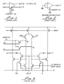
- FIG. 5 shows a schematic diagram of the differential amplifier with improved offset cancellation in accordance with the present invention.
- the transistors 501, 502, 503 are PMOS devices acting as a current source. Their gates are coupled to a BIAS voltage 505 generated from a separate BIAS circuit (not shown)
- the differential pair 510, 511 are also PMOS devices with their sources coupled to the drains of the PMOS 502.
- the input signals INM and INP are applied to the gates of the differential pair 510, 511, respectively. Coupled to the drains of the differential pair 510, 511 at branch pa and pb are the drains of load transistors 532, 533.
- One of the output signals, OUTM 520 appears at the node connecting the drain of PMOS 501, the drain of NMOS 523, and the drain of NMOS 536.
- the other output, OUTP 525 appears at the node connecting the drain of PMOS 503, the drain of NMOS 524 and the drain of NMOS 537.
- a calibration signal CAL 521 is applied to the gate of NMOS 530, which has its source connected to the source of NMOS 531 and the gate of NMOS 532.
- the complementary calibration CALB 522 is applied to the gates of NMOS transistors 523, 524. Note that the gate of NMOS 533 and the source of NMOS 531 are also coupled to common-mode circuitry (not shown), as will be understood by those skilled in the art.
- the floating current sources 514, 515 are connected between the branches pa and pb 513, 512, respectively, as previously described in connection with Figure 2, to apply a current of I.
- the calibration process begins with the signal Q going high to connect the current source 514. This will cause the output OUTP to gradually ramp down, until it flips to the other supply rail, thus crossing AGND. The current from current source 514 is therefore the current needed to cancel the offset voltage.
- the offset has the other polarity, then the maximum current will be reached without the output voltage level ever crossing AGND, since the output will reach and stay at the bottom rail.
- the other current source 515 will be connected by QB going high. Then the output voltage level OUTP will be ramped up to eventually cross AGND. The current from the current source 515 at this moment is therefore what is needed to cancel the offset.
- Figure 6 shows a symbolic representation of the differential amplifier with improved offset cancellation during calibration mode. As previously described, the two inputs are tied to AGND, while the output OUTP is checked for an AGND crossing to determine the current needed to cancel the output voltage offset.
Landscapes
- Engineering & Computer Science (AREA)
- Power Engineering (AREA)
- Amplifiers (AREA)
- Measurement Of Current Or Voltage (AREA)
Claims (12)
- Amplificateur différentiel avec annulation de décalage, ledit amplificateur différentiel ayant un décalage de tension de sortie prédéterminé, comprenant :caractérisé en ce que ledit amplificateur différentiel comprend, de plus :des premiers moyens formant source de courant (501, 502, 503) connectés à une alimentation positive (p) pour fournir un courant à travers ledit amplificateur différentiel ;une paire différentielle (510, 511) comprenant des bornes de source, de drain et de grille dans une configuration de source commune, ladite source commune étant couplée auxdits premiers moyens formant source de courant (501, 502, 503) ;des moyens formant charge active connectés auxdites bornes de drain de ladite paire différentielle (510, 511) ;des seconds moyens formant source de courant (514, 515) couplés auxdites deux bornes de drain de ladite paire différentielle (510, 511), respectivement, pour injecter et extraire des courants complémentaires auxdites bornes de drain, afin d'annuler ladite tension de décalage prédéterminée.
- Amplificateur différentiel selon la revendication 1, dans lequel lesdits seconds moyens formant source de courant (514, 515) comprennent, soit au moins une source de courant flottante, soit au moins deux sources de courant fixes avec des courants complémentaires.
- Amplificateur différentiel selon la revendication 2, dans lequel :
ladite paire différentielle (510, 511) comprend une paire de transistors PMOS. - Amplificateur différentiel selon la revendication 2, dans lequel :
ladite paire différentielle (510, 511) comprend une paire de transistors NMOS. - Amplificateur différentiel selon la revendication 1, dans lequel lesdits seconds moyens formant source de courant (514, 515) comprennent des première et seconde sources de courant pour injecter des courants dans ladite paire différentielle (510, 511) afin d'annuler ladite tension de décalage prédéterminée.
- Amplificateur différentiel selon la revendication 2, dans lequel lesdits moyens formant source de courant flottante (514, 515) comprennent des première et seconde sources de courant pour injecter des courants dans ladite paire différentielle (510, 511) et pour extraire des courants de celle-ci afin d'annuler ladite tension de décalage prédéterminée.
- Amplificateur différentiel selon la revendication 3, dans lequel lesdits moyens formant source de courant flottante (514, 515) comprennent des première et seconde sources de courant pour injecter des courants dans ladite paire différentielle (510, 511) et pour extraire des courants de celle-ci afin d'annuler ladite tension de décalage prédéterminée.
- Amplificateur différentiel selon la revendication 4, dans lequel lesdits moyens formant source de courant flottante (514, 515) comprennent des première et seconde sources de courant pour injecter des courants dans ladite paire différentielle (510, 511) et pour extraire des courants de celle-ci afin d'annuler ladite tension de décalage prédéterminée.
- Amplificateur différentiel avec annulation de décalage, ledit amplificateur différentiel ayant une tension de décalage prédéterminée, comprenant :caractérisé en ce que ledit amplificateur différentiel comprend, de plus :des moyens formant source de courant (501, 502, 503) couplés à une alimentation positive (p) pour fournir un courant à travers ledit amplificateur différentiel ;une paire différentielle (510, 511) comportant des bornes de source, de grille et de drain dans une configuration de source commune, leurs bornes de source commune étant couplées auxdits moyens formant source de courant (501, 502, 503) ;des moyens formant charge active couplés aux bornes de drain de ladite paire différentielle (510, 511) ;des premiers moyens formant source de courant (514) couplés à la borne de drain de ladite paire différentielle (510, 511) pour appliquer un premier courant à ladite paire différentielle, etune seconde source de courant (515), de même amplitude mais de direction opposée auxdits premiers moyens formant source de courant (514), couplée à une autre borne de drain de ladite paire différentielle (510, 511) pour appliquer un second courant audit amplificateur différentiel, dans lequel à la fois lesdits premier et second courants appliqués ensemble annulent ladite tension de décalage prédéterminée.
- Amplificateur différentiel selon la revendication 9, dans lequel :
ladite paire différentielle (510, 511) comprend une paire de transistors PMOS. - Amplificateur différentiel selon la revendication 9, dans lequel :
ladite paire différentielle (510, 511) comprend une paire de transistors NMOS. - Procédé d'annulation d'une tension de décalage prédéterminée dans un amplificateur différentiel, ledit amplificateur différentiel comprenant une première source de courant (501, 502, 503) connectée à une alimentation positive pour fournir un courant à travers ledit amplificateur différentiel, le procédé comprenant les étapes consistant à :(a) connecter une paire différentielle (510, 511) comprenant des bornes de source, de drain et de grille dans une configuration de source commune, ladite source commune étant couplée auxdits moyens formant première source de courant (501, 502, 503) ;(b) connecter une charge active auxdites bornes de drain de ladite paire différentielle (510, 511) ;
caractérisé par l'étape consistant à :(c) connecter une seconde source de courant (514, 515) auxdites bornes de drain de ladite paire différentielle (510, 511) pour fournir des courants complémentaires auxdites bornes de drain afin d'annuler ladite tension de décalage prédéterminée, ladite source de courant appliquant un courant prédéterminé à une borne de drain de ladite paire différentielle (510, 511) tout en extrayant un courant complémentaire dudit courant prédéterminé à partir d'une autre borne de drain.
Applications Claiming Priority (2)
| Application Number | Priority Date | Filing Date | Title |
|---|---|---|---|
| US08/536,331 US5631603A (en) | 1995-09-29 | 1995-09-29 | Offset cancellation for differential amplifiers |
| US536331 | 1995-09-29 |
Publications (2)
| Publication Number | Publication Date |
|---|---|
| EP0768751A1 EP0768751A1 (fr) | 1997-04-16 |
| EP0768751B1 true EP0768751B1 (fr) | 2002-01-16 |
Family
ID=24138075
Family Applications (1)
| Application Number | Title | Priority Date | Filing Date |
|---|---|---|---|
| EP96115661A Expired - Lifetime EP0768751B1 (fr) | 1995-09-29 | 1996-09-30 | Annulation améliorée de décalage de courant continu pour amplificateurs différentiels |
Country Status (4)
| Country | Link |
|---|---|
| US (1) | US5631603A (fr) |
| EP (1) | EP0768751B1 (fr) |
| JP (1) | JPH09130172A (fr) |
| DE (1) | DE69618523T2 (fr) |
Cited By (2)
| Publication number | Priority date | Publication date | Assignee | Title |
|---|---|---|---|---|
| TWI385922B (zh) * | 2007-10-03 | 2013-02-11 | Renesas Electronics Corp | 半導體電路 |
| CN105954563A (zh) * | 2016-05-16 | 2016-09-21 | 国电南瑞科技股份有限公司 | 基于电流求导和差分电流过零点识别拖尾电流的方法 |
Families Citing this family (15)
| Publication number | Priority date | Publication date | Assignee | Title |
|---|---|---|---|---|
| US6006169A (en) * | 1997-12-31 | 1999-12-21 | Intel Corporation | Method and apparatus for trimming an integrated circuit |
| US6072349A (en) * | 1997-12-31 | 2000-06-06 | Intel Corporation | Comparator |
| WO2002087073A2 (fr) * | 2001-04-24 | 2002-10-31 | Tripath Technology Inc. | Systeme d'auto-etalonnage pour decalage en continu destine a un amplificateur de commutation numerique |
| US6535030B1 (en) * | 2001-06-19 | 2003-03-18 | Xilinx, Inc. | Differential comparator with offset correction |
| WO2003003568A2 (fr) * | 2001-06-29 | 2003-01-09 | Infineon Technologies North America Corp. | Circuit a auto zero actif pour amplificateurs programmables en boucle ouverte a continuite temporelle |
| DE10142707A1 (de) * | 2001-08-31 | 2003-04-03 | Infineon Technologies Ag | Mehrstufiger Differenzverstärker mit CMFB-Schaltkreis |
| US7026866B2 (en) * | 2003-03-28 | 2006-04-11 | Tripath Technology, Inc. | DC offset self-calibration system for a switching amplifier |
| US7154421B2 (en) * | 2003-12-12 | 2006-12-26 | Telasic Communications, Inc. | DNL/INL trim techniques for comparator based analog to digital converters |
| US7142047B2 (en) * | 2004-11-29 | 2006-11-28 | Tripath Technology, Inc. | Offset cancellation in a switching amplifier |
| US7321259B1 (en) | 2005-10-06 | 2008-01-22 | Altera Corporation | Programmable logic enabled dynamic offset cancellation |
| US7541857B1 (en) | 2005-12-29 | 2009-06-02 | Altera Corporation | Comparator offset cancellation assisted by PLD resources |
| US7368968B1 (en) * | 2005-12-29 | 2008-05-06 | Altera Corporation | Signal offset cancellation |
| TW201134088A (en) | 2010-03-31 | 2011-10-01 | Sunplus Technology Co Ltd | Differential offset calibration circuit |
| US20220352857A1 (en) * | 2021-04-30 | 2022-11-03 | Sumitomo Electric Industries, Ltd. | Transimpedance amplifier circuit |
| US11888483B2 (en) * | 2022-04-05 | 2024-01-30 | Cypress Semiconductor Corporation | Clock signal conversion circuit for high-speed serial data controllers |
Family Cites Families (4)
| Publication number | Priority date | Publication date | Assignee | Title |
|---|---|---|---|---|
| US4806875A (en) * | 1988-05-11 | 1989-02-21 | Maxim Integrated Products | Precision operational amplifier |
| US4933642A (en) * | 1989-02-17 | 1990-06-12 | Linear Technology Corporation | CMOS chopper-stabilized operational amplifier using two differential amplifier pairs as input stages |
| US5047727A (en) * | 1989-09-20 | 1991-09-10 | Deutsche Itt Industries Gmbh | Offset-voltage-balancing operational amplifier |
| US5124663A (en) * | 1991-03-04 | 1992-06-23 | Motorola, Inc. | Offset compensation CMOS operational amplifier |
-
1995
- 1995-09-29 US US08/536,331 patent/US5631603A/en not_active Expired - Lifetime
-
1996
- 1996-09-27 JP JP8256242A patent/JPH09130172A/ja not_active Withdrawn
- 1996-09-30 EP EP96115661A patent/EP0768751B1/fr not_active Expired - Lifetime
- 1996-09-30 DE DE69618523T patent/DE69618523T2/de not_active Expired - Lifetime
Cited By (3)
| Publication number | Priority date | Publication date | Assignee | Title |
|---|---|---|---|---|
| TWI385922B (zh) * | 2007-10-03 | 2013-02-11 | Renesas Electronics Corp | 半導體電路 |
| CN105954563A (zh) * | 2016-05-16 | 2016-09-21 | 国电南瑞科技股份有限公司 | 基于电流求导和差分电流过零点识别拖尾电流的方法 |
| CN105954563B (zh) * | 2016-05-16 | 2018-09-28 | 国电南瑞科技股份有限公司 | 基于电流求导和差分电流过零点识别拖尾电流的方法 |
Also Published As
| Publication number | Publication date |
|---|---|
| JPH09130172A (ja) | 1997-05-16 |
| US5631603A (en) | 1997-05-20 |
| DE69618523T2 (de) | 2002-09-05 |
| EP0768751A1 (fr) | 1997-04-16 |
| DE69618523D1 (de) | 2002-02-21 |
Similar Documents
| Publication | Publication Date | Title |
|---|---|---|
| EP0768751B1 (fr) | Annulation améliorée de décalage de courant continu pour amplificateurs différentiels | |
| US5124663A (en) | Offset compensation CMOS operational amplifier | |
| EP1380101B1 (fr) | Circuit resonnant de mode commun a condensateur commute pour amplificateur differentiel sans courant de queue | |
| US6456159B1 (en) | CMOS operational amplifier | |
| US6624698B2 (en) | Low-voltage, broadband operational amplifier | |
| US5963156A (en) | Sample and hold circuit and method with common mode differential signal feedback for converting single-ended signals to differential signals | |
| US5663680A (en) | Chopper stabilized amplifier having an additional differential amplifier stage for improved noise reduction | |
| US6066985A (en) | Large swing input/output analog buffer | |
| US20100289568A1 (en) | Low-Noise, Low-Power, Low Drift Offset Correction in Operational and Instrumentation Amplifiers | |
| JPH0927722A (ja) | ゲイン可変増幅装置 | |
| EP1010237A1 (fr) | Amplificateur operationnel multivoie d'ordre eleve avec reduction de decalage dynamique, limitation du courant de saturation regulee et retour du courant pour une meilleure stabilite conditionnelle | |
| US4874969A (en) | High speed CMOS comparator with hysteresis | |
| JPH05152870A (ja) | 演算増幅器 | |
| US6396334B1 (en) | Charge pump for reference voltages in analog to digital converter | |
| US5798660A (en) | Cascoded differential pair amplifier with current injection for gain enhancement | |
| US20020105369A1 (en) | Clock buffer with DC offset suppression | |
| US6617921B2 (en) | High output swing comparator stage | |
| US5136255A (en) | Amplifier circuit | |
| EP0836275A1 (fr) | Amplificateur opérationnel commuté à haute vitesse pour applications à tension d'alimentation basse | |
| US5923206A (en) | Charge injection cancellation technique | |
| CN111669166B (zh) | 用于低偏移开关电容器积分器的开关方案 | |
| US6127855A (en) | Switch-capacitor circuit with overdrive-protected switch | |
| US7449950B2 (en) | Analog signal processing circuit | |
| US7888994B2 (en) | Differential to single-ended conversion circuit and comparator using the circuit | |
| US6480065B1 (en) | CMOS folding amplifier having high resolution and low power consumption |
Legal Events
| Date | Code | Title | Description |
|---|---|---|---|
| PUAI | Public reference made under article 153(3) epc to a published international application that has entered the european phase |
Free format text: ORIGINAL CODE: 0009012 |
|
| AK | Designated contracting states |
Kind code of ref document: A1 Designated state(s): DE FR GB |
|
| RIN1 | Information on inventor provided before grant (corrected) |
Inventor name: SHAMLOU, DARYUSH (NMI) Inventor name: MACROBBIE, EDWARD W. Inventor name: STUBBE, FREDERIC M. |
|
| 17P | Request for examination filed |
Effective date: 19971013 |
|
| 17Q | First examination report despatched |
Effective date: 19991216 |
|
| RAP1 | Party data changed (applicant data changed or rights of an application transferred) |
Owner name: CONEXANT SYSTEMS, INC. |
|
| GRAG | Despatch of communication of intention to grant |
Free format text: ORIGINAL CODE: EPIDOS AGRA |
|
| GRAG | Despatch of communication of intention to grant |
Free format text: ORIGINAL CODE: EPIDOS AGRA |
|
| GRAH | Despatch of communication of intention to grant a patent |
Free format text: ORIGINAL CODE: EPIDOS IGRA |
|
| GRAH | Despatch of communication of intention to grant a patent |
Free format text: ORIGINAL CODE: EPIDOS IGRA |
|
| GRAA | (expected) grant |
Free format text: ORIGINAL CODE: 0009210 |
|
| REG | Reference to a national code |
Ref country code: GB Ref legal event code: IF02 |
|
| AK | Designated contracting states |
Kind code of ref document: B1 Designated state(s): DE FR GB |
|
| REF | Corresponds to: |
Ref document number: 69618523 Country of ref document: DE Date of ref document: 20020221 |
|
| PLBE | No opposition filed within time limit |
Free format text: ORIGINAL CODE: 0009261 |
|
| STAA | Information on the status of an ep patent application or granted ep patent |
Free format text: STATUS: NO OPPOSITION FILED WITHIN TIME LIMIT |
|
| 26N | No opposition filed | ||
| REG | Reference to a national code |
Ref country code: GB Ref legal event code: 732E |
|
| REG | Reference to a national code |
Ref country code: FR Ref legal event code: TP |
|
| PGFP | Annual fee paid to national office [announced via postgrant information from national office to epo] |
Ref country code: DE Payment date: 20130919 Year of fee payment: 18 |
|
| PGFP | Annual fee paid to national office [announced via postgrant information from national office to epo] |
Ref country code: FR Payment date: 20130919 Year of fee payment: 18 Ref country code: GB Payment date: 20130919 Year of fee payment: 18 |
|
| REG | Reference to a national code |
Ref country code: DE Ref legal event code: R119 Ref document number: 69618523 Country of ref document: DE |
|
| GBPC | Gb: european patent ceased through non-payment of renewal fee |
Effective date: 20140930 |
|
| REG | Reference to a national code |
Ref country code: FR Ref legal event code: ST Effective date: 20150529 |
|
| PG25 | Lapsed in a contracting state [announced via postgrant information from national office to epo] |
Ref country code: GB Free format text: LAPSE BECAUSE OF NON-PAYMENT OF DUE FEES Effective date: 20140930 Ref country code: DE Free format text: LAPSE BECAUSE OF NON-PAYMENT OF DUE FEES Effective date: 20150401 |
|
| PG25 | Lapsed in a contracting state [announced via postgrant information from national office to epo] |
Ref country code: FR Free format text: LAPSE BECAUSE OF NON-PAYMENT OF DUE FEES Effective date: 20140930 |