EP0767478A1 - Safety circuit - Google Patents
Safety circuit Download PDFInfo
- Publication number
- EP0767478A1 EP0767478A1 EP95117767A EP95117767A EP0767478A1 EP 0767478 A1 EP0767478 A1 EP 0767478A1 EP 95117767 A EP95117767 A EP 95117767A EP 95117767 A EP95117767 A EP 95117767A EP 0767478 A1 EP0767478 A1 EP 0767478A1
- Authority
- EP
- European Patent Office
- Prior art keywords
- signal
- multivibrator
- safety circuit
- driver stage
- relays
- Prior art date
- Legal status (The legal status is an assumption and is not a legal conclusion. Google has not performed a legal analysis and makes no representation as to the accuracy of the status listed.)
- Granted
Links
Images
Classifications
-
- F—MECHANICAL ENGINEERING; LIGHTING; HEATING; WEAPONS; BLASTING
- F16—ENGINEERING ELEMENTS AND UNITS; GENERAL MEASURES FOR PRODUCING AND MAINTAINING EFFECTIVE FUNCTIONING OF MACHINES OR INSTALLATIONS; THERMAL INSULATION IN GENERAL
- F16P—SAFETY DEVICES IN GENERAL; SAFETY DEVICES FOR PRESSES
- F16P3/00—Safety devices acting in conjunction with the control or operation of a machine; Control arrangements requiring the simultaneous use of two or more parts of the body
- F16P3/18—Control arrangements requiring the use of both hands
- F16P3/20—Control arrangements requiring the use of both hands for electric control systems
-
- H—ELECTRICITY
- H01—ELECTRIC ELEMENTS
- H01H—ELECTRIC SWITCHES; RELAYS; SELECTORS; EMERGENCY PROTECTIVE DEVICES
- H01H47/00—Circuit arrangements not adapted to a particular application of the relay and designed to obtain desired operating characteristics or to provide energising current
- H01H47/002—Monitoring or fail-safe circuits
- H01H47/004—Monitoring or fail-safe circuits using plural redundant serial connected relay operated contacts in controlled circuit
- H01H47/005—Safety control circuits therefor, e.g. chain of relays mutually monitoring each other
Definitions
- the invention relates to a safety circuit with an actuating device for electrical devices, the actuating device being operable by means of two buttons or contact sets.
- electrical devices is to be understood as a versatile field of application, i. That is, the invention can be applied to all electrical safety devices with two separately monitored electrical buttons or contact sets, such as light grids, protective doors, for example on machine systems, emergency stop monitors, limit switching monitors, floor mats, light curtains and the like. Examples of machine systems include presses, punching devices, milling machines, lathes or elevators.
- the electrical Safety circuit works correctly, so that it is only possible to switch through to the consumer, ie switch on the dangerous operating state, but that, on the other hand, switching through is definitely prevented if any fault occurs within the circuit.
- the previously known electrical safety circuits either do not meet all the safety criteria or they are designed in such a complicated and complex manner that they require a very high cost and a safety risk can also be seen in the complexity of the construction.
- the invention has for its object to provide a generally suitable safety circuit that is very simple and clearly designed and therefore means low costs, but which withstands all safety criteria including the avoidance of any manipulation.
- the safety circuit consists essentially of two modules, namely a driver stage and an astable multivibrator or a multivibrator with the features specified in claim 1.
- An advantageous embodiment of the invention is that a capacitor is provided, which is dimensioned such that it stores the energy in the rest position, which is required to energize the flip-flop or the multivibrator during the actuation time of both buttons of a maximum of 500 ms supply.
- the driver stage is supplied with voltage V + and V- via the make contacts and the relays are activated.
- the capacitor is integrated in the multivibrator.
- the astable flip-flop or multivibrator square-wave signals with a slope produces up to 10 microseconds, preferably less than 1 s, in particular, a duty cycle, there is a T to 50% T of 50%.
- a first diode is arranged between the first button and the driver stage and a second diode between the second button and the driver stage, the diodes blocking the current flow to the driver stage when the buttons are not actuated.
- the square-wave signals of the multivibrator or multivibrator control the driver stage in such a way that the square-wave signals are alternately high or low, so that either the first or the second relay is energized.
- the flip-flop or the multivibrator are supplied via the relays when the relays are energized.
- the two complementary square-wave signals of the same length are constant and inverse to one another.
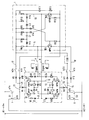
- the safety circuit shown in the drawing consists essentially of a driver stage 2 according to the rectangular dash-dotted line and a flip-flop or a multivibrator 1, which is also enclosed in the drawing by a rectangular dash-dotted line and to the driver stage 2, as explained in detail below is connected.
- Driver stage 2 interacts with two buttons S1 and S2 of an actuating device, not shown in detail, for example a two-hand actuation.
- the pushbuttons S1 and S2 should be operated at the same time if possible, at least within the short actuation time explained in more detail below.
- the driver stage 2 is supplied with the electrical voltage V + and V- via the buttons S1 and S2.
- Driver stage 2 has two PNP transistors Q1 and Q2 and two NPN transistors Q3 and Q4.
- the bases of the PNP transistor Q2 and the NPN transistor Q4 are connected to one another via a line 3, in which line 3 two resistors R2 and R4 and two Zener diodes Z2 and Z4 are connected in series.
- a line 4 is connected between the Zener diodes Z2 and Z4, which are connected in the same direction, in their forward direction from the resistor R4 to the resistor R2, which connects the driver stage 2 with the trigger circuit or the multivibrator 1 and that was explained in more detail below Signal 1 transmits, the line 4 in the multivibrator being connected to a line 5 which connects the resistor R6 to the collector of the transistor Q5.
- the collector of the PNP transistor Q2 is connected via a line 6 to the collector of the NPN transistor Q4.
- the emitter of the NPN transistor Q4 is in turn connected to the emitter of the NPN transistor Q3, the collector of which is connected via a line 7 to the collector of the PNP transistor Q1 is connected.
- the emitter of the PNP transistor Q1 is also connected to the emitter of the PNP transistor Q2.
- the PNP transistor Q1 and the NPN transistor Q3 are also connected via a line 8, which is connected to the bases of the aforementioned transistors Q1 and Q3, respectively.
- Two resistors R1 and R3 are arranged in line 8, between which Zener diodes Z1 and Z3 are connected.
- a line 9 is connected between the Zener diodes Z1 and Z3, which connects the line 8 in the driver stage 2 with a line 10 in the flip-flop or in the multivibrator 1, the line 10 between the resistor R11 and the collector of the NPN transistor Q6 runs.
- Signal 2 which will be explained below, is transmitted via line 9.
- the second relay-diode combination consists of a line 12, in which a diode V7 and a relay K2 are connected in series, the diode V7 on the collector side of the PNP transistor Q2 and the relay K2 on the collector side of the NPN transistor Q3 and the forward direction of the diode V7 runs from the collector of the PNP transistor Q2 to the collector of the NPN transistor Q3.
- a freewheeling diode V6 is also connected in parallel with the relay K2, the forward direction of which runs counter to the forward direction of the diode V7.
- the button S1 which in this example is equipped with a double contact, namely an NC contact s1ö and a NO contact s1s, is connected to the driver stage 2 via a line 13.
- the button S2 which is also equipped with a double contact, namely an NC contact s2ö and a NO contact s2s, is connected to the driver stage 2 via a line 14.
- Opener contacts a1ö and k2ö of relays K1 and K2 are arranged in lines 13 and 14, which also lead to the flip-flop or multivibrator 1, a diode V10 being connected to the normally closed contact k1ö and a diode V11 connected to the normally closed contact k2ö, the forward direction of which are oriented in opposite directions.
- further lines 17 and 18 run parallel to the lines 13 and 14, which likewise connect the button S1 on the one hand and the button S2 on the other hand to the flip-flop or the multivibrator 1.
- NO contacts k2s and k1s of the relays K2 and K1 are provided.
- the normally open contacts k2s and k1s are also connected upstream of diodes V9 and V12, which in turn are oriented in opposite directions with respect to their forward direction, the diodes V9 and V10 on the one hand and the diodes V11 and V12 on the other hand also being oriented in opposite directions.
- the driver stage 2 is connected via a line 21 to the line 13, the line 21 being connected between the emitters of the PNP transistors Q1 and Q2 and having a diode V1, the forward direction of which from the push button S1 to the connecting line between the emitters of the PNP Transistors Q1 and Q2 is aligned.
- a line 22 is provided which also has a diode V8 and which is connected on the emitter side to the NPN transistors Q3 and Q4, the diode V8 passing its direction from the emitters of the NPN transistors Q3 and Q4 to line 14.
- the flip-flop or multivibrator 1 has two NPN transistors Q5 and Q6, the bases of which are each connected between a resistor R5 or R12 and a diode V15 or V14.
- the collector of NPN transistor Q5 is connected in series with a resistor R6, whereas the collector of NPN transistor Q6 is connected in series with resistor R11.
- Resistor R6 is connected in parallel with two resistors R7 and R8 and resistor R11 is connected in parallel with two resistors R9 and R10.
- a diode V13 is connected between the resistors R6 and R7 and a diode V16 is connected between the resistors R10 and R11, the flow direction of the diode V13 from the resistor R7 to the resistor R6 and the flow direction of the diode V16 from the resistor R10 to the resistor R11.
- a capacitor C1 is connected between the resistors R7 and R8 and a capacitor C2 is connected between the resistors R9 and R10, the resistors R8 and R9 being connected in series with the diodes V14 and V 15, the direction of flow of which towards the bases of the NPN -Transistors Q5 and Q6 runs.
- a capacitor C3 and a resistor R13 are also connected in parallel with the resistor R11, the positive plate of the capacitor C3 being arranged on the side of the resistor R11 and the negative plate of the capacitor C3 being arranged on the side of the resistor R13, which has the emitter of the NPN transistor Q6 on the output side and the resistor R12 connected in parallel with it.
- the safety circuit uses direct current is operated. If the buttons S1 and S2 of the actuation device, for example a two-hand operation, are not pressed, the safety circuit is in the rest position. Via the closed contacts of the connection, referred to simply as ESB (external start condition), with feedback circuits known per se, namely the connection of the safety circuit to the rest of the machine control system, for example a dangerous metalworking machine, furthermore via the break contact k2ö of the relay K2, the diode V11 and the break contact s2ö of the button S2, the flip-flop or the multivibrator 1 is supplied with the voltage V-. Via the break contact k1ö of the relay K1, the diode V10 and the break contact s1ö of the button S1, the flip-flop or the multivibrator 1 is set to voltage V +.
- ESB internal start condition
- the flip-flop or multivibrator 1 swings in this state and generates two square-wave signals, namely signal 1 and signal 2, which are complementary and inverse to one another and each have the same length of time.
- the capacitor C3 absorbs or stores the energy which it needs in order to supply the flip-flop or the multivibrator 1 in an actuation time of the buttons S1 and S2 of a maximum of 500 ms. If the two buttons S1 and S2 are not actuated within this actuation time, i.e. practically simultaneously, the capacitor C3 is discharged prematurely, so that the multivibrator 1 or multivibrator 1 would no longer supply the relays K1 and K2, so that the further process the safety circuit would be interrupted.
- the diodes V1 and V8 block the current flow for the driver stage 2, so that the relays K1 and K2 are not energized. If a break contact k1ö and k2ö of the relays K1 or K2 are not closed in this state, the flip-flop or the multivibrator 1 would not work. Since the relays K1 and K2 positive relays, a possible contact failure is discovered here.
- driver stage 2 When pushbuttons S1 and S2 are actuated within the actuation time of 500 ms, driver stage 2 is supplied with voltage V + and V- via make contacts s1s and s2s. The diodes V1 and V8 are now polarized in the direction of flow. In this state, the energy stored in capacitor C3 supplies the flip-flop or multivibrator 1 for the maximum actuation time of 500 ms.
- relays K1 and K2 are activated and supply the flip-flop or multivibrator 1 with voltage via diodes V9 and V12.
- the square-wave signals signal 1 and signal 2 of the multivibrator or multivibrator 1 control the driver stage 2 as follows:
- signal 1 is high (high) and signal 2 low (low), as a result of which the transistors Q1 and Q 4 conduct and the relay K1 is excited, which also switches the contacts of the relay accordingly.
- signal 1 is low (low) and signal 2 is high (high), so that transistors Q2 and Q3 conduct and relay K2 is energized, so that its contacts switch accordingly.
- the flip-flop or the multivibrator 1 is supplied via the make contacts k1s and k2s of the relays K1 and K2.
- the current flows from A1 via the normally open contact s1s of the button S1, the diode V1, the transistor Q1, the diode V4 through the relay K1 to the transistor Q4 and from the transistor Q4 via the diode V8 and the normally open contact s2s of the button S2 to A1.
- the relay K1 is energized.
- the current flows from A1 via the normally open contact s1s of the button S1, the diode V1 to the transistor Q2 and from the transistor Q2 via the diode V7 through the relay K2 and from there via the transistor Q3 to the diode V8 to the normally open contact s2s of the button S2 to flow to A2.
- the relay K2 is energized.
- the frequency of the multivibrator or multivibrator 1 is preferably 1000 Hz and thus changes the state of the signals signal 1 and signal 2 every 0.5 ms. Due to the delay time of the relays K1 and K2 and the magnetic energy stored in the respective relay coil, which maintains the current flow of the mutual induction through the relay coils during the control breaks via the freewheeling diode V5 for relay K1 and the freewheeling diode V6 for relay K2 and K2 tightened. This state remains until the buttons S1 and S2 are released. Now the diodes V1 and V8 block the current flow and the driver stage 2 is no longer supplied with voltage. The relays K1 and K2 drop out, which sets the rest position of the device or the safety circuit.
- either the transistor Q5 or the transistor Q6 is turned on in the flip-flop or in the multivibrator 1 when it is switched on.
- the collector of transistor Q6 is at low potential in accordance with signal 2.
- a charging current, which is defined by the resistor R9, thus flows via the capacitor C2.
- the base of transistor Q5 is initially at low potential, transistor Q5 being blocked.
- the collector of transistor Q5 is correspondingly the signal 1 high potential.
- the charge current flowing through capacitor C2 increases the potential at the base of transistor Q5 until transistor Q5 turns on.
- Signal 1 drops to low potential and at the same time a charging current, which is defined by resistor R8, flows through capacitor C1.
- transistor Q6 falls back to low potential and blocks transistor Q6, causing signal 2 to go high.
- the diodes V13, V14, V15 and V16 present in the safety circuit described above serve to accelerate the switching times of signals 1 and 2.
- the operating points are set by resistors R5 and R12.
- the following error analysis shows further features and effects of the safety circuit according to the invention. Above all, the error analysis shows that all conceivable errors from pushbuttons S1, S2 to the input of the ESB (external star condition) of the external machine control system are recognized and that switching through is prevented in any case.
- the dangerous movement to be protected is triggered redundantly via two unsigned outputs of the safety device.
- the redundant outputs can be designed both as normally open circuits and as normally closed circuits.
Abstract
Description
Die Erfindung betrifft eine Sicherheitsschaltung mit einer Betätigungsvorrichtung für elektrische Einrichtungen, wobei die Betätigungsvorrichtung mittels zweier Taster bzw. Kontaktsätzen bedienbar ist. Unter dem Begriff elektrische Einrichtungen sind vielseitige Anwendungsgebiete zu verstehen, d. h., die Erfindung läßt sich auf alle elektrische Sicherheitseinrichtungen mit zwei getrennt zu überwachenden elektrischen Tastern bzw. Kontaktsätzen, wie bei Lichtgittern, Schutztüren, zum Beispiel an Maschinenanlagen, Not-Aus-Überwachungen, Grenzschaltüberwachungen, Fußmatten, Lichtvorhängen und dergleichen anwenden. Als Beispiele für Maschinenanlagen seien Pressen, Stanzvorrichtungen, Fräsmaschinen, Drehbänke oder Aufzüge genannt.The invention relates to a safety circuit with an actuating device for electrical devices, the actuating device being operable by means of two buttons or contact sets. The term electrical devices is to be understood as a versatile field of application, i. That is, the invention can be applied to all electrical safety devices with two separately monitored electrical buttons or contact sets, such as light grids, protective doors, for example on machine systems, emergency stop monitors, limit switching monitors, floor mats, light curtains and the like. Examples of machine systems include presses, punching devices, milling machines, lathes or elevators.
Aus der Praxis und aus dem Stand der Technik sind Sicherheitsschaltungen der zuvor genannten Gattung in mehreren Ausführungen bekannt, und zwar im Zusammenhang mit elektrischen Einrichtungen oder Maschinen, bei denen im eingeschalteten Zustand für die Bedienungspersonen gefährliche Bedingungen, insbesondere gefährliche Maschinenbewegungen herrschen. Zum Einschalten des jeweils gefährlichen Zustandes dient hierbei eine Zweihandbetätigung, wodurch sichergestellt werden soll, daß die beiden Hände der bedienenden Person beschäftigt sind und jede Möglichkeit ausgeschlossen ist, etwa mit der einen oder anderen Hand in den Gefahr bringenden Raum einzugreifen. Gleichzeitig soll sichergestellt sein, daß sich die bedienende Person oder deren Beine an einem Platz befinden, an dem keine Gefahr während der gefährlichen Bewegung auf die bedienende Person entsteht. In diesem Zusammenhang soll auch bei den bekannten Sicherheitsschaltungen angestrebt werden, daß jegliche Manipulation an der Zweihandbetätigung ausgeschlossen ist. Ferner wird angestrebt, daß die elektrische Sicherheitsschaltung fehlerfrei arbeitet, so daß nur dann ein Durchschalten an den Verbraucher, d. h. ein Einschalten des gefährlichen Betriebszustandes möglich ist, daß aber andererseits bei Auftreten irgendeines Fehlers innerhalb der Schaltung mit Sicherheit ein Durchschalten unterbunden wird. Die bisher bekannten elektrischen Sicherheitsschaltungen erfüllen entweder nicht alle Sicherheitskriterien oder sie sind derart kompliziert und bauaufwendig gestaltet, daß sie einen sehr hohen Kostenaufwand erfordern und auch gerade in der Kompliziertheit des Aufbaus ein Sicherheitsrisiko zu sehen ist.Several versions of safety circuits of the aforementioned type are known from practice and from the prior art, specifically in connection with electrical devices or machines in which dangerous conditions, in particular dangerous machine movements, prevail for the operators when switched on. A two-hand operation is used to switch on the respective dangerous condition, which is to ensure that the operator's two hands are busy and that every possibility is excluded, for example to intervene in the dangerous space with one hand or the other. At the same time, it should be ensured that the operator or his legs are in a place where there is no danger during the dangerous movement on the operator. In this context, it should also be attempted with the known safety circuits that any manipulation of the two-hand operation is excluded. It is also sought that the electrical Safety circuit works correctly, so that it is only possible to switch through to the consumer, ie switch on the dangerous operating state, but that, on the other hand, switching through is definitely prevented if any fault occurs within the circuit. The previously known electrical safety circuits either do not meet all the safety criteria or they are designed in such a complicated and complex manner that they require a very high cost and a safety risk can also be seen in the complexity of the construction.
Der Erfindung liegt die Aufgabe zugrunde, eine allgemein geeignete Sicherheitsschaltung zu schaffen, die sehr einfach und übersichtlich gestaltet ist und die einen demzufolge geringen Kostenaufwand bedeutet, die aber allen Sicherheitskriterien standhält einschließlich der Vermeidung von irgendwelchen Manipulationen.The invention has for its object to provide a generally suitable safety circuit that is very simple and clearly designed and therefore means low costs, but which withstands all safety criteria including the avoidance of any manipulation.
Zur Lösung dieser Aufgabe wird eine Sicherheitsschaltung mit den Merkmalen des Anspruches 1 vorgeschlagen.To achieve this object, a safety circuit with the features of
Demzufolge besteht die Sicherheitsschaltung im wesentlichen aus zwei Baugruppen, nämlich einer Treiberstufe und einer astabilen Kippstufe bzw. einem Multivibrator mit den im Anspruch 1 angeführten Merkmalen.Accordingly, the safety circuit consists essentially of two modules, namely a driver stage and an astable multivibrator or a multivibrator with the features specified in
Eine vorteilhafte Ausgestaltung der Erfindung besteht darin, daß ein Kondensator vorgesehen ist, welcher so bemessen ist, daß er in Ruhelage die Energie speichert, die benötigt wird, um in der Betätigungszeit beider Taster von maximal 500 ms die Kippstufe bzw. den Multivibrator mit Energie zu versorgen.An advantageous embodiment of the invention is that a capacitor is provided, which is dimensioned such that it stores the energy in the rest position, which is required to energize the flip-flop or the multivibrator during the actuation time of both buttons of a maximum of 500 ms supply.
In diesem Zusammenhang ist es von Vorteil, daß bei Betätigung der beiden Taster innerhalb einer Betätigungszeit von maximal 500 ms die Treiberstufe über die Schließerkontakte der Taster mit Spannung V+ und V- versorgt ist und die Relais aktiviert werden. Schaltungsmäßig ist der Kondensator in die Kippstufe bzw. den Multivibrator integriert.In this context, it is advantageous that when the two buttons are actuated within an actuation time of maximum 500 ms the driver stage is supplied with voltage V + and V- via the make contacts and the relays are activated. In terms of circuitry, the capacitor is integrated in the multivibrator.
Vorzugsweise erzeugt die astabile Kippstufe bzw. der Multivibrator Rechtecksignale mit einer Flankensteilheit bis zu 10 µs, vorzugsweise kleiner als 1 µs, wobei insbesondere ein Tastverhältnis Tein zu Taus von 50% zu 50% besteht.Preferably, the astable flip-flop or multivibrator square-wave signals with a slope produces up to 10 microseconds, preferably less than 1 s, in particular, a duty cycle, there is a T to 50% T of 50%.
Nach einem weiteren Merkmal der Erfindung ist vorgesehen, daß zwischen dem ersten Taster und der Treiberstufe eine erste Diode und zwischen dem zweiten Taster und der Treiberstufe eine zweite Diode angeordnet sind, wobei die Dioden bei unbetätigten Tastern den Stromfluß zur Treiberstufe sperren.According to a further feature of the invention it is provided that a first diode is arranged between the first button and the driver stage and a second diode between the second button and the driver stage, the diodes blocking the current flow to the driver stage when the buttons are not actuated.
Ferner ist es bei einer vorteilhaften Weiterbildung der erfindungsgemäßen Sicherheitsschaltung vorgesehen, daß die Rechtecksignale der Kippstufe bzw. des Multivibrators die Treiberstufe in der Art ansteuern, daß die Rechtecksignale alternierend hoch oder niedrig sind, so daß entweder das erste oder das zweite Relais erregt ist.Furthermore, it is provided in an advantageous development of the safety circuit according to the invention that the square-wave signals of the multivibrator or multivibrator control the driver stage in such a way that the square-wave signals are alternately high or low, so that either the first or the second relay is energized.
Nach einem weiteren Merkmal der Erfindung ist vorgesehen, daß die Kippstufe bzw. der Multivibrator über Schließer der Relais versorgt sind, wenn die Relais angezogen sind.According to a further feature of the invention, it is provided that the flip-flop or the multivibrator are supplied via the relays when the relays are energized.
Schließlich ist es bei der erfindungsgemäßen Sicherheitsschaltung vorgesehen, daß die zwei komplementären Rechtecksignale gleiche Längen andauernd und zueinander invers sind.Finally, it is provided in the safety circuit according to the invention that the two complementary square-wave signals of the same length are constant and inverse to one another.
In der Zeichnung ist eine bevorzugte Ausführungsform der erfindungsgemäßen Sicherheitsschaltung dargestellt, die nachfolgend in ihrem Aufbau und in ihrer Funktion beschrieben ist.In the drawing, a preferred embodiment of the safety circuit according to the invention is shown, which is described below in its structure and function.
Die in der Zeichnung dargestellte Sicherheitsschaltung besteht im wesentlichen aus einer Treiberstufe 2 gemäß der rechteckigen strichpunktierten Linie und einer Kippstufe bzw. einem Multivibrator 1, der ebenfalls in der Zeichnung von einer rechteckigen strichpunktierten Linie umschlossen ist und an die Treiberstufe 2, wie nachfolgend noch ausführlich dargelegt wird, angeschlossen ist.The safety circuit shown in the drawing consists essentially of a
Die Treiberstufe 2 wirkt mit zwei Tastern S1 und S2 einer im einzelnen nicht dargestellten Betätigungsvorrichtung, beispielsweise einer Zweihandbetätigung zusammen. Die Taster S1 und S2 sind möglichst gleichzeitig, zumindest innerhalb der weiter unten näher erläuterten kurzen Betätigungszeit, zu bedienen. Über die Taster S1 und S2 wird der Treiberstufe 2 die elektrische Spannung V+ sowie V- zugeführt. Die Treiberstufe 2 weist zwei PNP-Transistoren Q1 und Q2 und zwei NPN-Transistoren Q3 und Q4 auf. Die Basen des PNP-Transistors Q2 und des NPN-Transistors Q4 sind über eine Leitung 3 miteinander verbunden, wobei in dieser Leitung 3 zwei Widerstände R2 und R4 und zwei Zenerdioden Z2 und Z4 in Reihe geschaltet sind. Ferner ist zwischen den Zenerdioden Z2 und Z4, die gleichsinnig geschaltet sind, und zwar in ihrer Durchlaßrichtung vom Widerstand R4 zum Widerstand R2, eine Leitung 4 angeschlossen, die die Treiberstufe 2 mit der Kippstufe bzw. dem Multivibrator 1 verbindet und daß weiter unten näher erläuterte Signal 1 überträgt, wobei die Leitung 4 im Multivibrator an einer Leitung 5 angeschlossen ist, die den Widerstand R6 mit dem Kollektor des Transistors Q5 verbindet.
Ferner ist der Kollektor des PNP-Transistors Q2 über eine Leitung 6 mit dem Kollektor des NPN-Transistors Q4 verbunden. Der Emitter des NPN-Transistors Q4 ist wiederum mit dem Emitter des NPN-Transistors Q3 verbunden, dessen Kollektor über eine Leitung 7 mit dem Kollektor des PNP-Transistors Q1 verbunden ist. Der Emitter des PNP-Transistors Q1 ist ferner mit dem Emitter des PNP-Transistors Q2 verbunden. Der PNP-Transistor Q1 und der NPN-Transistor Q3 sind darüberhinaus über eine Leitung 8 verbunden, die jeweils an den Basen der voranstehend genannten Transistoren Q1 und Q3 angeschlossen ist. In der Leitung 8 sind zwei Widerstände R1 und R3 angeordnet, zwischen denen Zenerdioden Z1 und Z3 geschaltet sind. Zwischen den Zenerdioden Z1 und Z3 ist eine Leitung 9 angeschlossen, welche die Leitung 8 in der Treiberstufe 2 mit einer Leitung 10 in der Kippstufe bzw. in dem Multivibrator 1 verbindet, wobei die Leitung 10 zwischen dem Widerstand R11 und dem Kollektor des NPN-Transistors Q6 verläuft. Über die Leitung 9 wird das nachfolgend noch erläuterte Signal 2 übertragen.Furthermore, the collector of the PNP transistor Q2 is connected via a
Zwischen die Leitungen 6 und 7 sind zwei Relais-Dioden-Kombinationen geschaltet, wobei in einer Leitung 11 eine Diode V4 und ein Relais K1 geschaltet ist, wobei die Durchlaßrichtung dieser Diode von dem Kollektor des PNP-Transistors Q1 in Richtung auf den Kollektor des NPN-Transistors Q4 verläuft. Parallel zum Relais K1 ist eine Freilaufdiode V5 geschaltet, deren Durchlaßrichtung entgegengesetzt der Durchlaßrichtung der Diode V4 ist.Between the
Die zweite Relais-Dioden-Kombination besteht aus einer Leitung 12, in welcher eine Diode V7 und ein Relais K2 in Reihe geschaltet sind, wobei die Diode V7 kollektorseitig des PNP-Transistors Q2 und das Relais K2 kollektorseitig des NPN-Transistors Q3 angeordnet ist und die Durchlaßrichtung der Diode V7 vom Kollektor des PNP-Transistors Q2 zum Kollektor des NPN-Transistors Q3 verläuft. Parallel zum Relais K2 ist ferner eine Freilaufdiode V6 geschaltet, deren Durchlaßrichtung entgegengesetzt der Durchlaßrichtung der Diode V7 verläuft.The second relay-diode combination consists of a
Der Taster S1, welcher in diesem Beispiel mit einem Doppelkontakt, nämlich einem Öffnerkontakt s1ö und einem Schließerkontakt s1s ausgestattet ist, ist über eine Leitung 13 mit der Treiberstufe 2 verbunden. In gleicher Weise ist der Taster S2, der ebenfalls mit einem Doppelkontakt, nämlich einem Öffnerkontakt s2ö und einem Schließerkontakt s2s ausgestattet ist, über eine Leitung 14 mit der Treiberstufe 2 verbunden. In die Leitungen 13 und 14, die ebenfalls zu der Kippstufe bzw. dem Multivibrator 1 führen, sind Öffnerkontakte a1ö und k2ö der Relais K1 und K2 angeordnet, wobei dem Öffnerkontakt k1ö eine Diode V10 und dem Öffnerkontakt k2ö eine Diode V11 vorgeschaltet sind, deren Durchlaßrichtung entgegengesetzt ausgerichtet sind. Parallel zu den Leitungen 13 und 14 verlaufen gemäß diesem Ausführungsbeispiel weitere Leitungen 17 und 18, welche ebenfalls den Taster S1 einerseits und den Taster S2 andererseits mit der Kippstufe bzw. dem Multivibrator 1 verbinden. In die Leitungen 17 und 18 sind Schließerkontakte k2s und k1s der Relais K2 und K1 vorgesehen. Den Schließerkontakten k2s und k1s sind ebenfalls Dioden V9 und V12 vorgeschaltet, die wiederum hinsichtlich ihrer Durchlaßrichtung gegenläufig ausgerichtet sind, wobei ebenfalls die Dioden V9 und V10 einerseits und die Dioden V11 und V12 andererseits gegenläufig ausgerichtet sind.The button S1, which in this example is equipped with a double contact, namely an NC contact s1ö and a NO contact s1s, is connected to the
Die Treiberstufe 2 ist über eine Leitung 21 an die Leitung 13 angeschlossen, wobei die Leitung 21 zwischen den Emittern der PNP-Transistoren Q1 und Q2 angeschlossen ist und eine Diode V1 aufweist, deren Durchlaßrichtung vom Taster S1 zu der Verbindungsleitung zwischen den Emittern der PNP-Transistoren Q1 und Q2 ausgerichtet ist. Zwischen der Treiberstufe 2 und der Leitung 14 ist eine Leitung 22 vorgesehen, die ebenfalls eine Diode V8 aufweist und die emitterseitig an die NPN-Transistoren Q3 und Q4 angeschlossen ist, wobei die Diode V8 ihre Durchlaßrichtung von den Emittern der NPN-Transistoren Q3 und Q4 zur Leitung 14 hat.The
Die Kippstufe bzw. der Multivibrator 1 weist zwei NPN-Transistoren Q5 und Q6 auf, deren Basis jeweils zwischen einem Widerstand R5 bzw. R12 und jeweils einer Diode V15 bzw. V14 geschaltet ist. Der Kollektor des NPN-Transistors Q5 ist mit einem Widerstand R6 in Reihe geschaltet, wogegen der Kollektor des NPN-Transistors Q6 mit dem Widerstand R11 in Reihe geschaltet ist.The flip-flop or
Der Widerstand R6 ist parallel zu zwei Widerständen R7 und R8 und der Widerstand R11 ist parallel zu zwei Widerständen R9 und R10 geschaltet. Zwischen die Widerstände R6 und R7 ist eine Diode V13 und zwischen die Widerstände R10 und R11 ist eine Diode V16 geschaltet, wobei die Durchflußrichtung der Diode V13 vom Widerstand R7 zum Widerstand R6 und die Durchflußrichtung der Diode V16 vom Widerstand R10 zum Widerstand R11 verläuft.Resistor R6 is connected in parallel with two resistors R7 and R8 and resistor R11 is connected in parallel with two resistors R9 and R10. A diode V13 is connected between the resistors R6 and R7 and a diode V16 is connected between the resistors R10 and R11, the flow direction of the diode V13 from the resistor R7 to the resistor R6 and the flow direction of the diode V16 from the resistor R10 to the resistor R11.
Ferner sind zwischen die Widerstände R7 und R8 ein Kondensator C1 und zwischen die Widerstände R9 und R10 ein Kondensator C2 geschaltet, wobei die Widerstände R8 und R9 in Reihe mit den Dioden V14 und V 15 geschaltet sind, deren Durchflußrichtung in Richtung auf die Basen der NPN-Transistoren Q5 und Q6 verläuft.Furthermore, a capacitor C1 is connected between the resistors R7 and R8 and a capacitor C2 is connected between the resistors R9 and R10, the resistors R8 and R9 being connected in series with the diodes V14 and
Parallel zum Widerstand R11 ist ferner ein Kondensator C3 und ein Widerstand R13 geschaltet, wobei die positive Platte des Kondensators C3 seitens des Widerstandes R11 und die negative Platte des Kondensators C3 seitens des Widerstandes R13 angeordnet ist, welcher ausgangsseitig mit dem Emitter des NPN-Transistors Q6 und dem dazu parallel geschalteten Widerstand R12 verbunden ist.A capacitor C3 and a resistor R13 are also connected in parallel with the resistor R11, the positive plate of the capacitor C3 being arranged on the side of the resistor R11 and the negative plate of the capacitor C3 being arranged on the side of the resistor R13, which has the emitter of the NPN transistor Q6 on the output side and the resistor R12 connected in parallel with it.
Die Wirkungsweise der zuvor beschriebenen Sicherheitsschaltung ist im wesentlichen folgende:The principle of operation of the safety circuit described above is essentially as follows:
Zunächst sei bemerkt, daß die Sicherheitsschaltung gemäß dem beschriebenen Ausführungsbeispiel mit Gleichstrom betrieben wird. Wenn die Taster S1 und S2 der Betätigungsvorrichtung, beispielsweise einer Zweihandbetätigung nicht gedrückt sind, so befindet sich die Sicherheitsschaltung in Ruhelage. Über die geschlossenen Kontakte des vereinfacht mit ESB (externe Startbedingung) bezeichneten Anschlusses mit an sich bekannten Rückführkreisen, nämlich dem Anschluß der Sicherheitsschaltung an den Rest der Maschinensteuerung, beispielsweise einer Gefahr bringenden metallverarbeitenden Maschine, ferner über den Öffnerkontakt k2ö des Relais K2, die Diode V11 und den Öffnerkontakt s2ö des Tasters S2 wird die Kippstufe bzw. der Multivibrator 1 mit der Spannung V- versorgt. Über den Öffnerkontakt k1ö des Relais K1, die Diode V10 und den Öffnerkontakt s1ö des Tasters S1 wird die Kippstufe bzw. der Multivibrator 1 auf Spannung V+ gelegt.First of all, it should be noted that the safety circuit according to the described exemplary embodiment uses direct current is operated. If the buttons S1 and S2 of the actuation device, for example a two-hand operation, are not pressed, the safety circuit is in the rest position. Via the closed contacts of the connection, referred to simply as ESB (external start condition), with feedback circuits known per se, namely the connection of the safety circuit to the rest of the machine control system, for example a dangerous metalworking machine, furthermore via the break contact k2ö of the relay K2, the diode V11 and the break contact s2ö of the button S2, the flip-flop or the
Die Kippstufe bzw. der Multivibrator 1 schwingt in diesem Zustand an und erzeugt zwei Rechtecksignale, nämlich Signal 1 und Signal 2, die komplementär und zueinander invers verlaufen und jeweils gleiche Zeitlängen andauern. In dieser Ruhelage nimmt der Kondensator C3 die Energie auf bzw. speichert diese, die er benötigt, um in einer Betätigungszeit der Taster S1 und S2 von maximal 500 ms die Kippstufe bzw. den Multivibrator 1 zu versorgen. Wenn die beiden Taster S1 und S2 nicht innerhalb dieser Betätigungszeit, also praktisch gleichzeitig, betätigt werden, ist der Kondensator C3 vorzeitig entladen, so daß die Kippstufe bzw. der Multivibrator 1 die Relais K1 und K2 nicht mehr versorgen würde, so daß der weitere Vorgang der Sicherheitsschaltung unterbrochen würde. Die Dioden V1 und V8 sperren in diesem Zustand, in dem die Taster S1 und S2 unbetätigt sind, den Stromfluß für die Treiberstufe 2, so daß die Relais K1 und K2 nicht erregt werden. Wenn in diesem Zustand ein Öffnerkontakt k1ö und k2ö der Relais K1 oder K2 nicht geschlossen sind, würde die Kippstufe bzw. der Multivibrator 1 nicht arbeiten. Da die Relais K1 und K2 zwangsführende Relais sind, wird ein mögliches Kontaktversagen hier entdeckt.The flip-flop or
Bei Betätigung der Taster S1 und S2 innerhalb der Betätigungszeit von 500 ms wird die Treiberstufe 2 über die Schließer s1s und s2s mit Spannung V+ und V- versorgt. Die Dioden V1 und V8 sind jetzt in Flußrichtung gepolt. Die im Kondensator C3 gespeicherte Energie versorgt in diesem Zustand für die Länge der Betätigungszeit von maximal 500 ms die Kippstufe bzw. den Multivibrator 1.When pushbuttons S1 and S2 are actuated within the actuation time of 500 ms,
Bei der Betätigung der Taster S1 und S2 innerhalb der Betätigungszeit von maximal 500 ms werden die Relais K1 und K2 aktiviert und versorgen die Kippstufe bzw. den Multivibrator 1 über die Dioden V9 und V12 mit Spannung. Hierbei steuern die Rechtecksignale Signal 1 und Signal 2 der Kippstufe bzw. des Multivibrators 1 die Treiberstufe 2 wie folgt durch:When pushbuttons S1 and S2 are actuated within a maximum actuation time of 500 ms, relays K1 and K2 are activated and supply the flip-flop or
In einem ersten Zustand ist das Signal 1 hoch (high) und das Signal 2 niedrig (low), wodurch die Transistoren Q1 und Q 4 leiten und das Relais K1 erregt wird, womit auch die Kontakte des Relais entsprechend umschalten.In a first state,
In einem zweiten Zustand ist das Signal 1 niedrig (low) und das Signal 2 hoch (high), so daß die Transistoren Q2 und Q3 leiten und das Relais K2 erregt wird, womit dessen Kontakte entsprechend umschalten.In a second state,
Sind die Relais K1 und 2 angezogen, so wird die Kippstufe bzw. der Multivibrator 1 über die Schließerkontakte k1s und k2s der Relais K1 und K2 versorgt.If the relays K1 and 2 are energized, the flip-flop or the
Im vorstehend genannten ersten Zustand fließt der Strom von A1 über den Schließerkontakt s1s des Tasters S1, die Diode V1, den Transistor Q1, die Diode V4 durch das Relais K1 zum Transistor Q4 und von dem Transistor Q4 über die Diode V8 und den Schließerkontakt s2s des Tasters S2 nach A1. Hierbei wird das Relais K1 erregt.In the above-mentioned first state, the current flows from A1 via the normally open contact s1s of the button S1, the diode V1, the transistor Q1, the diode V4 through the relay K1 to the transistor Q4 and from the transistor Q4 via the diode V8 and the normally open contact s2s of the button S2 to A1. Here the relay K1 is energized.
In dem voranstehend beschriebenen zweiten Zustand fließt der Strom von A1 über den Schließerkontakt s1s des Tasters S1, die Diode V1 zum Transistor Q2 und vom Transistor Q2 über die Diode V7 durch das Relais K2 und von dort über den Transistor Q3 zur Diode V8, um über den Schließerkontakt s2s des Tasters S2 nach A2 zu fließen. In diesem Zustand wird das Relais K2 erregt.In the second state described above, the current flows from A1 via the normally open contact s1s of the button S1, the diode V1 to the transistor Q2 and from the transistor Q2 via the diode V7 through the relay K2 and from there via the transistor Q3 to the diode V8 to the normally open contact s2s of the button S2 to flow to A2. In this state, the relay K2 is energized.
Die Frequenz der Kippstufe bzw. des Multivibrators 1 beträgt vorzugsweise 1000 Hz und wechselt somit den Zustand der Signale Signal 1 und Signal 2 alle 0,5 ms. Bedingt durch die Abfallverzugszeit der Relais K1 und K2 und der in der jeweiligen Relaisspule gespeicherten magnetischen Energie, die in den Ansteuerpausen über die Freilaufdiode V5 für Relais K1 und die Freilaufdiode V6 für Relais K2 den Stromfluß der Gegeninduktion durch die Relaisspulen aufrechterhält, bleiben beide Relais K1 und K2 angezogen. Dieser Zustand bleibt solange erhalten, bis die Taster S1 und S2 losgelassen werden. Nun sperren die Dioden V1 und V8 den Stromfluß und die Treiberstufe 2 wird nicht mehr mit Spannung versorgt. Die Relais K1 und K2 fallen ab, wodurch sich die Ruhelage des Gerätes bzw. der Sicherheitsschaltung einstellt.The frequency of the multivibrator or
Aufgrund verschiedener Toleranzen wird bei der Kippstufe bzw. bei dem Multivibrator 1 im Einschaltmoment entweder der Transistor Q5 oder der Transistor Q6 durchgesteuert. Für den Fall, daß der Transistor Q6 durchgesteuert ist, liegt der Kollektor des Transistors Q6 entsprechend dem Signal 2 auf low-Potential. Damit fließt ein Ladestrom, der durch den Widerstand R9 definiert ist, über den Kondensator C2. Die Basis des Transistors Q5 liegt hierbei zunächst auf low-Potential, wobei der Transistor Q5 gesperrt ist. Hierdurch steht am Kollektor des Transistors Q5 entsprechend dem Signal 1 high-Potential an. Durch den Ladestrom, der über den Kondensator C2 fließt, steigt das Potential an der Basis des Transistors Q5 an, bis der Transistor Q5 durchsteuert. Dabei fällt das Signal 1 auf low-Potential und gleichzeitig fließt ein Ladestrom, der durch den Widerstand R8 definiert ist, über den Kondensator C1.Due to different tolerances, either the transistor Q5 or the transistor Q6 is turned on in the flip-flop or in the
Die Basis des Transistors Q6 fällt dabei zurück auf low-Potential und sperrt den Transistor Q6, wodurch das Signal 2 auf high-Potential geht.The base of transistor Q6 falls back to low potential and blocks transistor Q6, causing
Dieser Prozeß läuft zyklisch ab. Sofern![]()
![]()
Die in der voranstehend beschriebenen Sicherheitsschaltung vorhandenen Dioden V13, V14, V15 und V16 dienen der Beschleunigung der Umschaltzeiten der Signale 1 und 2. Die Arbeitspunkte werden durch die Widerstände R5 und R12 eingestellt.The diodes V13, V14, V15 and V16 present in the safety circuit described above serve to accelerate the switching times of
Aus der nachfolgenden Fehlerbetrachtung ergeben sich weitere Merkmale und Wirkungsweisen der erfindungsgemäßen Sicherheitsschaltung. Die Fehlerbetrachtung zeigt vor allem, daß alle nur denkbaren Fehler von den Tastern S1, S2 bis hin zum Eingang der ESB (externen Starbedingung) der externen Maschinensteuerung erkannt werden und in jedem Falle ein Durchschalten verhindert wird.The following error analysis shows further features and effects of the safety circuit according to the invention. Above all, the error analysis shows that all conceivable errors from pushbuttons S1, S2 to the input of the ESB (external star condition) of the external machine control system are recognized and that switching through is prevented in any case.
Die zu schützende gefährliche Bewegung wird über zwei nicht gezeichnete Ausgänge der Sicherheitseinrichtung redundant ausgelöst. Dabei können die redundanten Ausgänge sowohl als Schließerkreise als auch als Öffnerkreise ausgebildet sein.


Claims (10)
Priority Applications (7)
| Application Number | Priority Date | Filing Date | Title |
|---|---|---|---|
| EP95117767A EP0767478B1 (en) | 1995-10-04 | 1995-11-11 | Safety circuit |
| AT95117767T ATE185448T1 (en) | 1995-10-04 | 1995-11-11 | SAFETY CIRCUIT |
| DE59506997T DE59506997D1 (en) | 1995-10-04 | 1995-11-11 | Safety circuit |
| MXPA/A/1996/004549A MXPA96004549A (en) | 1995-10-04 | 1996-10-03 | Circuito de seguri |
| CA002187101A CA2187101C (en) | 1995-10-04 | 1996-10-03 | Safety circuit |
| US08/725,715 US5771146A (en) | 1995-10-04 | 1996-10-04 | Safety circuit |
| JP8264941A JPH09223427A (en) | 1995-10-04 | 1996-10-04 | Safety circuit having actuator for electric appliance |
Applications Claiming Priority (3)
| Application Number | Priority Date | Filing Date | Title |
|---|---|---|---|
| EP95115622 | 1995-10-04 | ||
| DE95115622 | 1995-10-04 | ||
| EP95117767A EP0767478B1 (en) | 1995-10-04 | 1995-11-11 | Safety circuit |
Publications (2)
| Publication Number | Publication Date |
|---|---|
| EP0767478A1 true EP0767478A1 (en) | 1997-04-09 |
| EP0767478B1 EP0767478B1 (en) | 1999-10-06 |
Family
ID=26138842
Family Applications (1)
| Application Number | Title | Priority Date | Filing Date |
|---|---|---|---|
| EP95117767A Expired - Lifetime EP0767478B1 (en) | 1995-10-04 | 1995-11-11 | Safety circuit |
Country Status (6)
| Country | Link |
|---|---|
| US (1) | US5771146A (en) |
| EP (1) | EP0767478B1 (en) |
| JP (1) | JPH09223427A (en) |
| AT (1) | ATE185448T1 (en) |
| CA (1) | CA2187101C (en) |
| DE (1) | DE59506997D1 (en) |
Cited By (2)
| Publication number | Priority date | Publication date | Assignee | Title |
|---|---|---|---|---|
| WO2001039229A1 (en) * | 1999-11-25 | 2001-05-31 | Siemens Aktiengesellschaft | Configuration comprising two contactors connected in series |
| EP2551874A1 (en) * | 2011-07-28 | 2013-01-30 | PHOENIX CONTACT GmbH & Co. KG | Electric relay control circuit |
Families Citing this family (1)
| Publication number | Priority date | Publication date | Assignee | Title |
|---|---|---|---|---|
| DE19715098B4 (en) * | 1997-04-11 | 2004-12-23 | Schneider Electric Gmbh | monitoring circuit |
Citations (3)
| Publication number | Priority date | Publication date | Assignee | Title |
|---|---|---|---|---|
| DE1926607A1 (en) * | 1969-05-24 | 1970-12-17 | Ako Werke Gmbh & Co | Elasticated wound dressing plasters with abrasive covers |
| EP0105054A1 (en) * | 1982-10-01 | 1984-04-11 | Square D Starkstrom GmbH | Circuit for the active control of limit switches arranged in pairs |
| DE3600173A1 (en) * | 1986-01-07 | 1987-07-09 | Rohr Manfred | Two-channel, two-handed circuit operated using direct current for power-operated presses or the like |
Family Cites Families (6)
| Publication number | Priority date | Publication date | Assignee | Title |
|---|---|---|---|---|
| DE1463215B2 (en) * | 1963-02-20 | 1970-12-17 | Th. Kieserling & Albrecht, 565O Solingen | Electrical safety control for presses, punching or the like |
| US3371254A (en) * | 1965-10-01 | 1968-02-27 | Harold T. Hagfors | Safety control system |
| US3793533A (en) * | 1973-03-16 | 1974-02-19 | Precision Electronic Component | Electrical safety control circuit |
| US3914621A (en) * | 1974-10-07 | 1975-10-21 | Gen Electric | Circuit for enabling safe actuation of a machine |
| US4412268A (en) * | 1981-10-02 | 1983-10-25 | Dart Industries Inc. | Safety switch system for industrial machines |
| US5235217A (en) * | 1991-07-24 | 1993-08-10 | Isb Ltd. | Capacitive press control actuation system |
-
1995
- 1995-11-11 DE DE59506997T patent/DE59506997D1/en not_active Expired - Lifetime
- 1995-11-11 EP EP95117767A patent/EP0767478B1/en not_active Expired - Lifetime
- 1995-11-11 AT AT95117767T patent/ATE185448T1/en not_active IP Right Cessation
-
1996
- 1996-10-03 CA CA002187101A patent/CA2187101C/en not_active Expired - Fee Related
- 1996-10-04 US US08/725,715 patent/US5771146A/en not_active Expired - Lifetime
- 1996-10-04 JP JP8264941A patent/JPH09223427A/en active Pending
Patent Citations (3)
| Publication number | Priority date | Publication date | Assignee | Title |
|---|---|---|---|---|
| DE1926607A1 (en) * | 1969-05-24 | 1970-12-17 | Ako Werke Gmbh & Co | Elasticated wound dressing plasters with abrasive covers |
| EP0105054A1 (en) * | 1982-10-01 | 1984-04-11 | Square D Starkstrom GmbH | Circuit for the active control of limit switches arranged in pairs |
| DE3600173A1 (en) * | 1986-01-07 | 1987-07-09 | Rohr Manfred | Two-channel, two-handed circuit operated using direct current for power-operated presses or the like |
Cited By (4)
| Publication number | Priority date | Publication date | Assignee | Title |
|---|---|---|---|---|
| WO2001039229A1 (en) * | 1999-11-25 | 2001-05-31 | Siemens Aktiengesellschaft | Configuration comprising two contactors connected in series |
| US6870723B1 (en) | 1999-11-25 | 2005-03-22 | Siemens Aktiengesellschaft | Configuration comprising two contactors connected in series |
| EP2551874A1 (en) * | 2011-07-28 | 2013-01-30 | PHOENIX CONTACT GmbH & Co. KG | Electric relay control circuit |
| DE102011052251A1 (en) * | 2011-07-28 | 2013-01-31 | Phoenix Contact Gmbh & Co. Kg | Electric relay drive circuit |
Also Published As
| Publication number | Publication date |
|---|---|
| DE59506997D1 (en) | 1999-11-11 |
| CA2187101C (en) | 2000-08-29 |
| CA2187101A1 (en) | 1997-04-05 |
| US5771146A (en) | 1998-06-23 |
| JPH09223427A (en) | 1997-08-26 |
| EP0767478B1 (en) | 1999-10-06 |
| ATE185448T1 (en) | 1999-10-15 |
| MX9604549A (en) | 1998-10-31 |
Similar Documents
| Publication | Publication Date | Title |
|---|---|---|
| DE10011211B4 (en) | Safety relay and safety relay system | |
| EP1493064B1 (en) | Device for the error-proof switching off of an electric consumer, particularly in industrial production plants | |
| DE19813143A1 (en) | Emergency switching system for motors, e.g. for use in robots and machine tools | |
| DE2711416C2 (en) | Arrangement for displaying the switching status of the switches | |
| DE102008002758B4 (en) | relay circuit | |
| DE2007664A1 (en) | Control circuit for machines | |
| EP0767478B1 (en) | Safety circuit | |
| DE19513191C1 (en) | Safety circuit with electronic switches across contacts of relays for human operative protection on equipment and machines | |
| DE19715098B4 (en) | monitoring circuit | |
| EP0470441A2 (en) | Method for communication of an acknowledgement signal for operating a robot | |
| EP0253000B1 (en) | Machine protective system | |
| DE2449725C3 (en) | Two-hand safety switch arrangement for switching on a machine and for triggering a reciprocating working stroke | |
| DE2524789A1 (en) | SAFETY DEVICE FOR METAL WORKING MACHINERY, IN PARTICULAR PRESSES AND PRESS BRAKES | |
| DE19751674C2 (en) | Circuit arrangement with safety function | |
| DE825698C (en) | Equipment for signal boxes with electrical locks, in particular table lever mechanisms | |
| EP0890058B1 (en) | Protective circuit | |
| DE2614748A1 (en) | Circuit to monitor function of indirectly acting switch - having reversing switch assigned to each switch position formed from 2 diodes in antiparallel | |
| EP1652203B1 (en) | Protector suitable for cascade connections and corresponding method for safety-conditioned switching | |
| DE19722927C1 (en) | Switching device with in-built safety function for protecting personnel from injury due to moving machinery or plant | |
| DE3637037A1 (en) | Set of points with local electrical control | |
| EP1451651A2 (en) | Electric motor drive for a piece of furniture | |
| DE2808761A1 (en) | Machine operator's safety circuit - has alternator producing control signal via control branch with gate connections controlled by two keys | |
| DE4424285A1 (en) | Two-channel, two-hand safety operating system for use with presses | |
| DE1135555B (en) | Device for central antivalence monitoring of electronic controls | |
| DE2318072B2 (en) | System for monitoring and error messages in safety systems |
Legal Events
| Date | Code | Title | Description |
|---|---|---|---|
| PUAI | Public reference made under article 153(3) epc to a published international application that has entered the european phase |
Free format text: ORIGINAL CODE: 0009012 |
|
| AK | Designated contracting states |
Kind code of ref document: A1 Designated state(s): AT BE CH DE DK ES FR GB GR IE IT LI LU MC NL PT SE |
|
| 17P | Request for examination filed |
Effective date: 19970821 |
|
| GRAG | Despatch of communication of intention to grant |
Free format text: ORIGINAL CODE: EPIDOS AGRA |
|
| GRAG | Despatch of communication of intention to grant |
Free format text: ORIGINAL CODE: EPIDOS AGRA |
|
| GRAH | Despatch of communication of intention to grant a patent |
Free format text: ORIGINAL CODE: EPIDOS IGRA |
|
| 17Q | First examination report despatched |
Effective date: 19990319 |
|
| GRAH | Despatch of communication of intention to grant a patent |
Free format text: ORIGINAL CODE: EPIDOS IGRA |
|
| GRAA | (expected) grant |
Free format text: ORIGINAL CODE: 0009210 |
|
| AK | Designated contracting states |
Kind code of ref document: B1 Designated state(s): AT BE CH DE DK ES FR GB GR IE IT LI LU MC NL PT SE |
|
| PG25 | Lapsed in a contracting state [announced via postgrant information from national office to epo] |
Ref country code: SE Free format text: THE PATENT HAS BEEN ANNULLED BY A DECISION OF A NATIONAL AUTHORITY Effective date: 19991006 Ref country code: NL Free format text: LAPSE BECAUSE OF FAILURE TO SUBMIT A TRANSLATION OF THE DESCRIPTION OR TO PAY THE FEE WITHIN THE PRESCRIBED TIME-LIMIT Effective date: 19991006 Ref country code: GR Free format text: LAPSE BECAUSE OF NON-PAYMENT OF DUE FEES Effective date: 19991006 Ref country code: ES Free format text: THE PATENT HAS BEEN ANNULLED BY A DECISION OF A NATIONAL AUTHORITY Effective date: 19991006 |
|
| REF | Corresponds to: |
Ref document number: 185448 Country of ref document: AT Date of ref document: 19991015 Kind code of ref document: T |
|
| REG | Reference to a national code |
Ref country code: CH Ref legal event code: EP |
|
| PG25 | Lapsed in a contracting state [announced via postgrant information from national office to epo] |
Ref country code: LU Free format text: LAPSE BECAUSE OF NON-PAYMENT OF DUE FEES Effective date: 19991111 Ref country code: AT Free format text: LAPSE BECAUSE OF NON-PAYMENT OF DUE FEES Effective date: 19991111 |
|
| REF | Corresponds to: |
Ref document number: 59506997 Country of ref document: DE Date of ref document: 19991111 |
|
| PG25 | Lapsed in a contracting state [announced via postgrant information from national office to epo] |
Ref country code: LI Free format text: LAPSE BECAUSE OF NON-PAYMENT OF DUE FEES Effective date: 19991130 Ref country code: CH Free format text: LAPSE BECAUSE OF NON-PAYMENT OF DUE FEES Effective date: 19991130 Ref country code: BE Free format text: LAPSE BECAUSE OF NON-PAYMENT OF DUE FEES Effective date: 19991130 |
|
| ITF | It: translation for a ep patent filed |
Owner name: STUDIO JAUMANN P. & C. S.N.C. |
|
| PG25 | Lapsed in a contracting state [announced via postgrant information from national office to epo] |
Ref country code: PT Free format text: LAPSE BECAUSE OF FAILURE TO SUBMIT A TRANSLATION OF THE DESCRIPTION OR TO PAY THE FEE WITHIN THE PRESCRIBED TIME-LIMIT Effective date: 20000106 Ref country code: DK Free format text: LAPSE BECAUSE OF FAILURE TO SUBMIT A TRANSLATION OF THE DESCRIPTION OR TO PAY THE FEE WITHIN THE PRESCRIBED TIME-LIMIT Effective date: 20000106 |
|
| ET | Fr: translation filed | ||
| GBT | Gb: translation of ep patent filed (gb section 77(6)(a)/1977) |
Effective date: 19991224 |
|
| REG | Reference to a national code |
Ref country code: IE Ref legal event code: FG4D Free format text: GERMAN |
|
| NLV1 | Nl: lapsed or annulled due to failure to fulfill the requirements of art. 29p and 29m of the patents act | ||
| BERE | Be: lapsed |
Owner name: SCHNEIDER ELECTRIC G.M.B.H. Effective date: 19991130 |
|
| PG25 | Lapsed in a contracting state [announced via postgrant information from national office to epo] |
Ref country code: MC Free format text: LAPSE BECAUSE OF NON-PAYMENT OF DUE FEES Effective date: 20000531 |
|
| REG | Reference to a national code |
Ref country code: CH Ref legal event code: PL |
|
| PLBE | No opposition filed within time limit |
Free format text: ORIGINAL CODE: 0009261 |
|
| STAA | Information on the status of an ep patent application or granted ep patent |
Free format text: STATUS: NO OPPOSITION FILED WITHIN TIME LIMIT |
|
| REG | Reference to a national code |
Ref country code: IE Ref legal event code: FD4D |
|
| 26N | No opposition filed | ||
| REG | Reference to a national code |
Ref country code: GB Ref legal event code: IF02 |
|
| REG | Reference to a national code |
Ref country code: FR Ref legal event code: CJ Ref country code: FR Ref legal event code: CD Ref country code: FR Ref legal event code: CA |
|
| PGFP | Annual fee paid to national office [announced via postgrant information from national office to epo] |
Ref country code: GB Payment date: 20101020 Year of fee payment: 16 Ref country code: IT Payment date: 20101125 Year of fee payment: 16 |
|
| GBPC | Gb: european patent ceased through non-payment of renewal fee |
Effective date: 20121111 |
|
| PG25 | Lapsed in a contracting state [announced via postgrant information from national office to epo] |
Ref country code: IT Free format text: LAPSE BECAUSE OF NON-PAYMENT OF DUE FEES Effective date: 20121111 |
|
| PG25 | Lapsed in a contracting state [announced via postgrant information from national office to epo] |
Ref country code: GB Free format text: LAPSE BECAUSE OF NON-PAYMENT OF DUE FEES Effective date: 20121111 |
|
| PGFP | Annual fee paid to national office [announced via postgrant information from national office to epo] |
Ref country code: DE Payment date: 20141014 Year of fee payment: 20 Ref country code: FR Payment date: 20141010 Year of fee payment: 20 |
|
| REG | Reference to a national code |
Ref country code: DE Ref legal event code: R071 Ref document number: 59506997 Country of ref document: DE |