EP0763402B1 - Method and apparatus for polishing semiconductor substrate - Google Patents
Method and apparatus for polishing semiconductor substrate Download PDFInfo
- Publication number
- EP0763402B1 EP0763402B1 EP96113864A EP96113864A EP0763402B1 EP 0763402 B1 EP0763402 B1 EP 0763402B1 EP 96113864 A EP96113864 A EP 96113864A EP 96113864 A EP96113864 A EP 96113864A EP 0763402 B1 EP0763402 B1 EP 0763402B1
- Authority
- EP
- European Patent Office
- Prior art keywords
- platen
- slurry
- polishing pad
- polishing
- semiconductor substrate
- Prior art date
- Legal status (The legal status is an assumption and is not a legal conclusion. Google has not performed a legal analysis and makes no representation as to the accuracy of the status listed.)
- Expired - Lifetime
Links
Images


Classifications
-
- B—PERFORMING OPERATIONS; TRANSPORTING
- B24—GRINDING; POLISHING
- B24B—MACHINES, DEVICES, OR PROCESSES FOR GRINDING OR POLISHING; DRESSING OR CONDITIONING OF ABRADING SURFACES; FEEDING OF GRINDING, POLISHING, OR LAPPING AGENTS
- B24B37/00—Lapping machines or devices; Accessories
- B24B37/04—Lapping machines or devices; Accessories designed for working plane surfaces
-
- B—PERFORMING OPERATIONS; TRANSPORTING
- B24—GRINDING; POLISHING
- B24B—MACHINES, DEVICES, OR PROCESSES FOR GRINDING OR POLISHING; DRESSING OR CONDITIONING OF ABRADING SURFACES; FEEDING OF GRINDING, POLISHING, OR LAPPING AGENTS
- B24B57/00—Devices for feeding, applying, grading or recovering grinding, polishing or lapping agents
- B24B57/02—Devices for feeding, applying, grading or recovering grinding, polishing or lapping agents for feeding of fluid, sprayed, pulverised, or liquefied grinding, polishing or lapping agents
Description
- The present invention relates to a method and apparatus for polishing a semiconductor substrate whereby chemical mechanical polishing (CMP) is performed with respect to a semiconductor substrate of silicon or the like to flatten a surface thereof.
- From the 1990s, CMP technology for polishing semiconductor substrates of silicon or the like has shown increasing tendencies toward single-wafer processing as the semiconductor substrates processed by CMP have had larger diameters on the order of 10 cm or more, resulting in an increased amount of slurry consumed per wafer.
- By way of example, a conventional apparatus for polishing a semiconductor substrate will be described below with reference to the drawings.
- FIG. 22 schematically shows the construction of the conventional polishing apparatus, in which is shown a
platen 11 including: asubstrate holder 11a made of a rigid material and having a flat surface; arotary shaft 11b extending vertically downwardly from the back surface of thesubstrate holder 11a; and rotating means (not shown) for rotating therotary shaft 11b. To the top surface of thesubstrate holder 11a of theplaten 11 is adhered apolishing pad 12. Above theplaten 11 is provided asubstrate holding head 14 which holds and rotates asemiconductor substrate 13. Thesemiconductor substrate 13 is rotated and pressed against thepolishing pad 12 on theplaten 11 by thesubstrate holding head 14. Aslurry 15 containing abrasive grains (extremely fine powder for polishing) is dropped in a prescribed amount from aslurry supply pipe 16 onto thepolishing pad 12 so as to supply the abrasive grains to the space between thepolishing pad 12 and thesemiconductor substrate 13. - In the polishing apparatus thus constructed, the
polishing pad 12 supplied with theslurry 15 is rotated by rotating theplaten 11 and thesemiconductor substrate 13 is pressed against the rotatingpolishing pad 12 by thesubstrate holding head 14 so that a surface of thesemiconductor substrate 13 is polished. - In this process, if the surface of the
semiconductor substrate 13 is rugged, the polishing rate is increased at projecting portions of thesemiconductor substrate 13 since their contact pressure with thepolishing pad 12 is high. On the other hand, the polishing rate is reduced at recessed portions of thesemiconductor substrate 13 since their contact pressure with thepolishing pad 12 is low. Consequently, the surface of thesemiconductor substrate 13 becomes less rugged and more smooth. - However, the above polishing apparatus have the following problems.
- When a consideration is given to the amount of supplied slurry and the polishing rate, the polishing rate increases with increases in the amount of supplied
slurry 15 and eventually becomes constant when the amount of supplied slurry reaches a given value. Accordingly, the amount ofslurry 15 normally supplied onto thepolishing pad 12 is slightly larger than the given value with which the polishing rate becomes constant. - However, since the
slurry 15 is supplied onto the rotatingpolishing pad 12 as described above, theslurry 15 is caused to flow to the peripheral portion of thepolishing pad 12 by a centrifugal force accompanying the rotation of theplaten 11. When the amount ofslurry 15 becomes smaller than the given value, the polishing rate is reduced. To compensate for the reduction in the polishing rate, the pressure for pressing thesemiconductor substrate 13 against thepolishing pad 12 should be increased. However, the increased pressure induces dishing or like phenomenon, which causes such a problem as the degradation of polishing properties. Hence, the slurry should constantly be supplied in an amount slightly larger than the given value with which the polishing rate becomes constant, so that the cost of the slurry accounts for a considerable proportion of the cost of polishing. - To solve the problem, there have been proposed an apparatus and method for polishing wherein a slurry on a polishing pad is prevented from flowing out by a partition board enclosing the polishing pad, as disclosed in U.S. Pat. No.4,910,155.
- According to the apparatus and method for polishing, however, foreign matters such as tips of polishing pad generated at the polishing are accumulated on the polishing pad. Also, water supplied onto the polishing pad to clean up a semiconductor substrate after polishing or perform dressing (the conditioning of the surface of the polishing pad) as well as the slurry is prevented from flowing out, resulting in unfavorable variations in the concentration of the slurry, which changes the polishing properties.
- Document EP-A-O 763 401, published on 19.03.1997 and which constitutes state of the art according to Art 54(3) EPC is regarded as the most relevant state of the art. This document proposes several solutions to the retention of the slurry on the platen, among which an apparatus for polishing a semiconductor substrate comprising:
- a platen having a flat surface and rotating around a shaft vertical to said flat surface;
- a polishing pad disposed on said flat surface of said platen;
- slurry supplying means for supplying a slurry onto said polishing pad;
- substrate holding means for holding a semiconductor substrate (13) and pressing it against said polishing pad; and
- a slurry pushing plate for pushing, to a central portion of said platen, the slurry supplied onto said polishing pad and caused to flow to a peripheral portion of said platen by a centrifugal force accompanying the rotation of said platen; wherein said slurry pushing plate is a pushing plate held over said polishing pad to push, to the central portion of said platen the slurry brought in contact therewith by the centrifugal force accompanying the rotation of said platen.
-
- This document also proposes
- an apparatus for polishing a semiconductor substrate comprising
- a platen having a flat surface and rotating around a shaft vertical to said flat surface;
- a polishing pad disposed on said flat surface of said platen;
- slurry supplying means for supplying a slurry onto said polishing pad;
- substrate holding means for holding a semiconductor substrate and pressing it against said polishing pad;
- slurry pushing means for pushing, to a central portion of said platen, the slurry supplied onto said polishing pad and caused to flow to a peripheral portion of said platen by a centrifugal force accompanying the rotation of said platen, wherein said slurry pushing means has a rotary member provided in contact with or slightly spaced from a top surface of said polishing pad and rotating in a direction opposite to the rotation of said platen.
-
- The present invention is defined by the apparatus claims 1,3,4, 6 and 7, as well as by the method claims 11, 12, 13 and 14. Preferred embodiments are defined in the dependent claims.
-
- FIG. 1 is a perspective view of an apparatus for polishing a semiconductor substrate according to a first embodiment;
- FIG. 2 is a perspective view of an apparatus for polishing a semiconductor substrate according to a second embodiment;
- FIG. 3 is a plan view of the apparatus for polishing a semiconductor substrate according to the second embodiment;
- FIG. 4 is a plan view showing a variation of a pushing plate in the apparatus for polishing a semiconductor substrate according to the second embodiment;
- FIGS. 5(a) to 5(d) are plan views showing respective variations of the pushing plate in the apparatus for polishing a semiconductor substrate according to the second embodiment;
- FIGS. 6(a) to 6(d) are cross-sectional views showing the respective variations of the pushing plate in the apparatus for polishing a semiconductor substrate according to the second embodiment;
- FIGS. 7(a) to 7(c) are perspective views illustrating a polishing method using the apparatus for polishing a semiconductor substrate according to the second embodiment;
- FIG. 8 is a perspective view of an apparatus for polishing a semiconductor substrate according to a third embodiment;
- FIG. 9 is a plan view illustrating polishing performed by using the apparatus for polishing the semiconductor substrate according to the third embodiment;
- FIG. 10 is a plan view showing a variation of a rotary member in the apparatus for polishing a semiconductor substrate according to the third embodiment;
- FIG. 11 is a perspective view of an apparatus for polishing a semiconductor substrate according to a fourth embodiment;
- FIG. 12 is a plan view of the apparatus for polishing a semiconductor substrate according to the fourth embodiment;
- FIGS. 13(a) to 13(d) are plan views showing respective variations of a pushing plate in the apparatus for polishing a semiconductor substrate according to the fourth embodiment;
- FIGS. 14(a) and 14(b) are perspective views each illustrating a polishing method using the apparatus for polishing a semiconductor substrate according to the fourth embodiment;
- FIGS. 15(a) and 15(b) are perspective views each illustrating the polishing method using the apparatus for polishing a semiconductor substrate according to the fourth embodiment;
- FIG. 16(a) is a perspective view of an apparatus for polishing a semiconductor substrate according to a fifth embodiment and FIG. 16(b) is a perspective view illustrating a polishing method using the apparatus for polishing a semiconductor substrate according to the fifth embodiment;
- FIGS. 17(a) and 17(b) are plan views illustrating the polishing method using the apparatus for polishing a semiconductor substrate according to the fifth embodiment;
- FIGS. 18(a) and 18(b) are plan views illustrating a polishing method using a variation of the apparatus for polishing a semiconductor substrate according to the fifth embodiment;
- FIG. 19 is a perspective view of an apparatus for polishing a semiconductor substrate according to a sixth embodiment;
- FIG. 20 is a perspective view of a polishing method using the apparatus for polishing a semiconductor substrate according to the sixth embodiment;
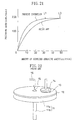
- FIG. 21 is a view showing respective relationships between the amounts of slurry and polishing rates during polishing performed by using the apparatus for polishing a semiconductor substrate according to the present invention and a conventional apparatus for polishing a semiconductor substrate; and
- FIG. 22 is a schematic perspective view of the conventional apparatus for polishing a semiconductor substrate.
-
- Below, polishing methods and polishing apparatus according to the individual embodiments of the present invention will be described with reference to the drawings.
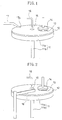
- FIG. 1 is a schematic perspective view of a polishing apparatus according to a first embodiment of the present invention, in which is shown a
platen 11 including: a polishing-pad holder 11a made of a rigid material and having a flat surface; arotary shaft 11b extending vertically downwardly from the back surface of the polishing-pad holder 11a; and rotating means (not shown) for rotating therotary shaft 11b. To the top surface of the polishing-pad holder 11a is adhered apolishing pad 12 made of polyurethane or like material. Above theplaten 11, there is provided asubstrate holding head 14 which holds and rotates asemiconductor substrate 13. Thesemiconductor substrate 13 is rotated and pressed against thepolishing pad 12 on theplaten 11 by thesubstrate holding head 14. Aslurry 15 containing abrasive grains is dropped in a prescribed amount from aslurry supply pipe 16 onto thepolishing pad 12 and supplied to the space between the polishingpad 12 and thesemiconductor substrate 13 by rotating theplaten 11 and thesubstrate holding head 14. - The first embodiment is characterized in that a compressed-
air supply pipe 17 for ejecting a compressed air to the top surface of thepolishing pad 12 is provided as slurry pushing means over the periphery of thepolishing pad 12. Anejection hole 17a of the compressed-air supply pipe 17 is opened to face the center of rotation of theplaten 11. Theejection hole 17a has a diameter of, e.g., about 3 mm and the flow speed of the compressed air ejected from theejection hole 17a is set at about 5 m/second. With the arrangement, the compressed air ejected from theejection hole 17a of the compressed-air supply pipe 17 is supplied from theslurry supply pipe 16 to the top surface of thepolishing pad 12 to push theslurry 15 directed to the peripheral portion by a centrifugal force accompanying the rotation of theplaten 11 back to the central portion of theplaten 11. As a result, theslurry 15 reciprocates between the central and peripheral portions of theplaten 11 to equally provide the abrasive grains over the top surface of thesemiconductor substrate 13. - The diameter of the
ejection hole 15a and the flow speed of the compressed air are not limited to the foregoing. Any diameter and any speed may be selected properly provided that theslurry 15 on thepolishing pad 12 is pushed back to the central portion of theplaten 11. Although theejection hole 17a of the compressed-air supply pipe 17 is opened to face the center of rotation of theplaten 11, it may face any direction provided that the gas ejected from theejection hole 17a is capable of causing theslurry 15 on thepolishing pad 12 to flow to the center of rotation of theplaten 11. - The number of
ejection holes 17a of the compressed-air supply pipe 17 is not particularly limited. However, a plurality of, e.g., 5 or 6ejection holes 17a are preferably provided. - Although the first embodiment has used the compressed air as the gas to be ejected, similar effects are achieved by using any other gas. However, an inert gas such as a nitrogen gas is preferably ejected depending on the type of the slurry, since the inert gas exhibits chemical stability to the slurry.
- Although the
slurry 15 contains the abrasive grains in the above first embodiment, theslurry 15 may be a liquid containing no abrasive grain. Any flowable slurry may be used extensively. The same shall apply to each of the embodiments which will be described below. - FIGS. 2 and 3 schematically show the construction of a polishing apparatus according to a second embodiment of the present invention, of which FIG. 2 is a perspective view and FIG. 3 is a plan view.
- The second embodiment comprises: a
platen 11; apolishing pad 12; asubstrate holding head 14; and aslurry supply pipe 16, similarly to the first embodiment. Asemiconductor substrate 13 is rotated and pressed against thepolishing pad 12 on theplaten 11. Aslurry 15 is supplied in a prescribed amount from theslurry supply pipe 16 onto thepolishing pad 12. - The second embodiment is characterized in that a slat-like
slurry pushing member 18 made of, e.g., polyurethane foam is provided as the slurry pushing means for pushing theslurry 15 to the central portion of theplaten 11 by sliding over thepolishing pad 12. As shown in FIG. 3, theslurry pushing member 18 is fixed such that aninner portion 18a thereof in a radial direction of theplaten 11 is positioned downstream (forward) of anouter portion 18b thereof in the radial direction of theplaten 11 in the direction of rotation of theplaten 11 during polishing. Specifically, theslurry pushing member 18 is fixed such that the tangent L to the circle S centering around the center of rotation of theplaten 11 and theslurry pushing member 18 intersect each other to form an angle of 120° therebetween. - With the arrangement, the
slurry 15 supplied from theslurry supply pipe 16 onto thepolishing pad 12 and caused to flow to the outside of theplaten 11 by a centrifugal force accompanying the rotation of theplaten 11 is returned to the central portion of theplaten 11 by the surface of theslurry pushing member 18, evenly spread over thepolishing pad 12, and supplied to thesemiconductor substrate 13. In the case of removing a cleaning liquid such as water from the top surface of thepolishing pad 12, the removal is promoted if theplaten 11 is rotated in the direction opposite to the rotation of theplaten 11 during polishing, since the cleaning liquid is brought in contact with the back surface of theslurry pushing member 18 by the rotation of theplaten 11 in the opposite direction. - The length and angle of the
slurry pushing member 18 may be selected properly provided that theslurry pushing member 18 returns theslurry 15 on thepolishing pad 12 to the central portion of theplaten 11. - Although the angle between the
slurry pushing member 18 and a radius of theplaten 11 is invariable in the second embodiment, the angle between theslurry pushing member 18 and a radius of theplaten 11 may be variable such that theslurry 15 is returned efficiently to the central portion of theplaten 11 depending on the viscosity of theslurry 15 and on the rotation speed of theplaten 11. - Although the
slurry pushing member 18 is fixed, it may be rotated in a direction relatively opposite to the rotation of theplaten 11 during polishing. In this case, it is necessary to provide theslurry pushing member 18 of such a length in such a position as to prevent theslurry pushing member 18 from colliding with thesubstrate holding head 14. In the arrangement, the cleaning liquid supplied onto thepolishing pad 12 can be removed efficiently by the back surface of theslurry pushing member 18. - The material of the
slurry pushing member 18 is not limited to polyurethane foam but any other material may be used instead. However, the use of a soft material such as one containing polyethylene, polypropylene, polystyrene, polyvinyl chloride, or Teflon as the main component or rubber such as butadiene rubber is particularly preferred, since theslurry pushing member 18 made of such a material is deformed to follow the surface configuration of thepolishing pad 12, as shown in FIG. 4. - There may be provided a space sufficiently large to permit the
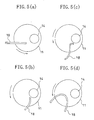
slurry 15 to be returned to the central portion of the platen 11 (space with a height equal to or less than the thickness of the layer of the slurry 15) between theslurry pushing member 18 and thepolishing pad 12 so that theslurry pushing member 18 is kept from rubbing against thepolishing pad 12. The arrangement is preferred since it is free from powder resulting from the rubbing of theslurry pushing member 18 against thepolishing pad 12. - FIGS. 5(a) to 5(d) and FIGS. 6(a) to 6(d) show variations of the
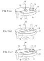
slurry pushing member 18 in terms of the configuration and number thereof. As shown in the drawings, the configuration and number of theslurry pushing members 18 are not limited but can be changed properly depending on the viscosity of theslurry 15 and the rotation speed of theplaten 11. As shown in FIG. 5(b) or 5(c), theslurry pushing member 18 may be curved such that the outer portion thereof in the radial direction of theplaten 11 has the function of collecting theslurry 15 and that the inner portion thereof in the radial direction of theplaten 11 has the function of pushing the collectedslurry 15 toward thesubstrate holding head 14. - Below, a polishing method using the polishing apparatus according to the second embodiment will be described with reference to FIGS. 7.
- Initially, as shown in FIG. 7(a), the
semiconductor substrate 13 is attached to thesubstrate holding head 14 with a face to be polished facing downward. - Next, as shown in FIG. 7(b), the
slurry 15 is supplied from theslurry supply pipe 16 onto a portion of thepolishing pad 12 corresponding to the near-central portion of theplaten 11, while theplaten 11 and thesubstrate holding head 14 are rotated counterclockwise (CCW). As a result, theslurry 15 is caused to flow to the peripheral portion of thepolishing pad 12 by a centrifugal force accompanying the rotation of theplaten 11 to be supplied to the interface between thesemiconductor substrate 13 and thepolishing pad 12. - As shown in FIG. 7(c), the
slurry 15 on thepolishing pad 12 tends to flow toward the outside of thepolishing pad 12 due to the centrifugal force accompanying the rotation of theplaten 11. However, theslurry 15 is brought in contact with theslurry pushing member 18 in one complete rotation of theplaten 11 and returned to the central portion of thepolishing pad 12 to be reused in the polishing of thesemiconductor substrate 13. - When the polishing of the
semiconductor substrate 13 is completed, a cleaning liquid such as water is supplied onto thepolishing pad 12 to clean the surface to be polished of thesemiconductor substrate 13 and remove theslurry 15 from the top surface of thepolishing pad 12. Thereafter, theplaten 11 is rotated clockwise (CW) to remove the slurry remaining on theplaten 11 and polishingpad 12. As a result, the cleaning liquid is pushed to the outside of thepolishing pad 12 so that the cleaning liquid is removed more efficiently than in the case where theslurry pushing member 18 is not provided. - Although the
platen 11 and thesubstrate holding head 14 are rotated after theslurry 15 is supplied in the foregoing polishing method, the timing of rotating theplaten 11 and thesubstrate holding head 14 and the timing of supplying theslurry 15 can be changed as necessary provided that theslurry 15 is supplied prior to the rotation of theplaten 11. - Although the
platen 11 is rotated CCW during polishing and CW during the removal of the cleaning liquid, the polishing effect by theslurry 15 remains substantially the same even when theplaten 11 is continuously rotated CCW during the removal of the cleaning liquid, except for a slight reduction in the speed at which the cleaning liquid is removed. - The
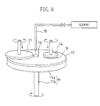
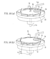
slurry 15 may be supplied onto a portion other than the portion of thepolishing pad 12 corresponding to the near-central portion of theplaten 11 provided that it is interior to the outer end of theslurry pushing member 18. - FIG. 8 is a perspective view schematically showing the construction of the polishing apparatus according to a third embodiment of the present invention. The third embodiment comprises: a
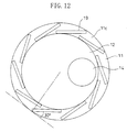
platen 11; apolishing pad 12; asubstrate holding head 14; and aslurry supply pipe 16, similarly to the first embodiment. Asemiconductor substrate 13 is rotated and pressed against thepolishing pad 12 on theplaten 11. Aslurry 15 is supplied in a prescribed amount from theslurry supply pipe 16 onto thepolishing pad 12. - The third embodiment is characterized in that a
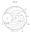
circular rotary member 21 as rotatable slurry pushing means is provided in close contact with or slightly spaced from the top surface of thepolishing pad 12 on the side opposite to thesubstrate holding head 14. The diameter of therotary member 21 is determined to be larger than the diameter of thesubstrate holding head 14. Therotary member 21 partially projects from the edge of thepolishing pad 12. Therotary member 21 rotates in the direction opposite to the rotation of theplaten 11 during polishing, while rotating in the same direction as the rotation of theplaten 11 during the removal of the cleaning liquid or the like. - Thus, as shown in FIG. 9, the
slurry 15 supplied from theslurry supply pipe 16 onto thepolishing pad 12 and directed to the peripheral portion of theplaten 11 by a centrifugal force accompanying the rotation of theplaten 11 is brought in contact with the outer circumferential surface of therotary member 21, returned to the central portion of theplaten 11 along the outer circumferential surface of therotary member 21, and evenly spread over thepolishing pad 12 to be supplied to thesemiconductor substrate 13. The arrow above thepolishing pad 12 in FIG. 9 conceptually indicates the flow direction of theslurry 15 during polishing. In this case, although theslurry 15 is formed into aswell 15a by the surface tension thereof on the peripheral portion of thepolishing pad 12, theswell 15a is eventually pushed back to the central portion of theplaten 11 during the rotation of therotary member 21 since therotary member 21 partially projects from the edge of thepolishing pad 12. - In removing the cleaning liquid from the top surface of the
polishing pad 12, on the other hand, the removal of the cleaning liquid is promoted since the cleaning liquid flows to the outside of theplaten 11 along the outer circumferential surface of therotary member 21 rotating in the same direction as theplaten 11. - The plan configuration of the
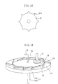
rotary member 21 is not limited to a circle. The provision of projectingportions 21a on the outer circumferential surface of therotary member 21 enhances the effect of pushing theslurry 15 back to the central portion of theplaten 11 along the outer circumferential surface of therotary member 21 rotating in the direction opposite to the rotation of theplaten 11. Although thededicated rotary member 21 is provided as the slurry pushing means in the third embodiment, a rotary member of the same configuration as that of thesubstrate holding head 14 may be provided in place of thededicated rotary member 21. - FIGS. 11 and 12 schematically show the construction of a polishing apparatus according to a fourth embodiment of the present invention, of which FIG. 11 is a perspective view and FIG. 12 is a plan view.
- The fourth embodiment comprises: a
platen 11; apolishing pad 12; asubstrate holding head 14; and aslurry supply pipe 16, similarly to the first embodiment. Asemiconductor substrate 13 is rotated and pressed against thepolishing pad 12. Aslurry 15 is supplied in a prescribed amount from theslurry supply pipe 16 onto thepolishing pad 12. - The fourth embodiment is characterized in that the diameter of the
polishing pad 12 is smaller than that of theplaten 11 so that thepolishing pad 12 is disposed on the central portion of theplaten 11. On the other hand, a plurality of slat-likeslurry holding members 19 made of, e.g., polyvinyl chloride are provided as slurry holding means along the outer circumferential surface of thepolishing pad 12 to hold theslurry 15 on thepolishing pad 12. Each of theslurry holding members 19 has such a height that the top position thereof is higher in level than the top surface of thepolishing pad 12 and is positioned so that the inner portion thereof in a radial direction of the platen 1 is downstream of the outer portion thereof in the radial direction of the platen 1 in the direction of rotation of the platen 1 during polishing. Specifically, theslurry holding member 19 is fixed so that an angle of about 30 degrees is formed between theslurry holding member 19 and a tangent to the outer circumferential surface of thepolishing pad 12. - As a general rule in the second embodiment, the
slurry pushing member 18 does not rotate in conjunction with thepolishing pad 12 so that theslurry 15 is pushed back to the central portion of theplaten 11. As a general rule in the fourth embodiment, on the other hand, theslurry holding members 19 rotate in conjunction with thepolishing pad 12 so that theslurry 15 is stored on thepolishing pad 12. Specifically, theslurry 15 supplied from theslurry supply pipe 16 onto thepolishing pad 12 and directed to the peripheral portion of theplaten 11 by a centrifugal force accompanying the rotation of theplaten 11 changes its direction in collision with theslurry holding members 19 and is stored on thepolishing pad 12. Consequently, theslurry 15 is evenly spread over thepolishing pad 12 when it is supplied to thesemiconductor substrate 13. - The proper length and angle of the
slurry holding member 19 can be selected such that theslurry 15 is held on thepolishing pad 12. If any adjacent two of the holdingmembers 19 are provided to overlap in the radial direction of theplaten 11, theslurry 15 can be held more positively. - The
slurry holding member 19 may be provided on thepolishing pad 12, not on the peripheral portion 11c of theplaten 11. - The material of the
slurry holding members 19 is not limited to polyvinyl chloride. Any other material can be used instead, similarly to the second embodiment. - FIGS. 13(a) to 13(d) show variations of the configuration, placement angle, and number of the
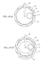
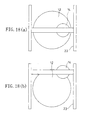
slurry holding member 19. As shown in the drawings, the configuration, placement angle, and number of theslurry holding member 19 are not particularly limited and can be varied properly depending on the viscosity of theslurry 15 and on the rotation speed of theplaten 11. In other words, theslurry holding member 19 may be curved. - Below, a polishing method using the polishing apparatus according to the fourth embodiment will be described with reference to FIGS. 14(a) and 14(b) and FIGS. 15(a) and 15(b).
- Initially, as shown in FIGS. 14(a), the
semiconductor substrate 13 is attached to thesubstrate holding head 14 with a surface to the polished facing downward and pressed against thepolishing pad 12. - Next, as shown in FIG. 14(b), the
slurry 15 is supplied from theslurry supply pipe 16 onto a portion of thepolishing pad 12 corresponding to the near-central portion of theplaten 11, followed by the clockwise (CW) rotation of theplaten 11 andsubstrate holding head 14. As a result, theslurry 15 flows toward the outside of thepolishing pad 12 due to the centrifugal force accompanying the rotation of theplaten 11 to be supplied to the interface between thesemiconductor substrate 13 and thepolishing pad 12. - As shown in FIG. 15(a), the
slurry 15 on thepolishing pad 12 tends to flow toward the outside of thepolishing pad 12 due to the centrifugal force accompanying the rotation of theplaten 11, comes into contact with the inner surface of eachslurry holding member 19, flows upstream in the direction of rotation of the platen 11 (from the outer portion of eachslurry holding member 19 in the radial direction of thepolishing pad 12 to the inner portion of theslurry holding member 19 in the radial direction of the polishing pad 12) along the inner surface of theslurry holding member 19, and then moves to the outer portion of the subsequentslurry holding member 19 in the radial direction of thepolishing pad 12. By repeatedly performing the foregoing flowing movement, theslurry 15 is held on thepolishing pad 12 and reused in the polishing of thesemiconductor substrate 13. - When the polishing of the
semiconductor substrate 13 is completed, a cleaning liquid such as water is supplied onto thepolishing pad 12 to clean the polished surface of thesemiconductor substrate 13 and rinse theslurry 15 out of the top surface of polishingpad 12. Thereafter, theplaten 11 is rotated counterclockwise (CCW) to remove the cleaning liquid or the like remaining on theplaten 11 and on thepolishing pad 12. As a result, the cleaning liquid 20 exhibits a flowing movement in the direction opposite to the flowing movement of theslurry 15 described above as shown in FIG. 15(b), so that the cleaningliquid 20 is removed more efficiently than in the case where noslurry holding member 19 is provided. - Although the
platen 11 is rotated CW during the polishing of thesemiconductor substrate 13 and CCW during the removal of the cleaningliquid 20, theplaten 11 is rotated CCW during the polishing of thesemiconductor substrate 13 and CW during the removal of the cleaningliquid 20 in the case where the orientation in which theslurry holding member 19 is placed is radially reversed. - FIG. 16(a) is a schematic perspective view of a polishing apparatus according to a fifth embodiment of the present invention.
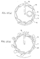
- As shown in FIG. 16(a), the fifth embodiment also comprises a
platen 11, apolishing pad 12, asubstrate holding head 14, and aslurry supply pipe 16, similarly to the first embodiment. Asemiconductor substrate 13 is rotated and pressed against thepolishing pad 12 on theplaten 11. Aslurry 15 is supplied in a prescribed amount from theslurry supply pipe 16 onto thepolishing pad 12. In FIG. 16(a), the drawing of a polishing-pad holder 11a of theplaten 11 is omitted. - The fifth embodiment is characterized in that a ring-shaped vertically
movable member 22 moving vertically relative to theplaten 11 and rotated by rotating means other than the rotating means for theplaten 11 is provided on the outside of the polishing-pad holder 11a of theplaten 11. On the verticallymovable member 22, a plurality of slat-likeslurry holding members 19 having the same configuration as in the fourth embodiment is provided as the slurry holding means along the outer circumferential surface of thepolishing pad 12 to hold theslurry 15 on thepolishing pad 12. Theslurry holding members 19 move vertically relative to thepolishing pad 12 as the verticallymovable member 22 moves vertically. Theslurry holding member 19 is held such that the top position thereof becomes higher in level than the surface of thepolishing pad 12 during polishing and that the top position thereof becomes lower in level than the surface of thepolishing pad 12 during cleaning. - The fifth embodiment is also characterized in that an
arm 14a of thesubstrate holding head 14 performs a rotary movement over the surface of thepolishing pad 12. - The two-dimensional arrangement of the
slurry holding members 19 is the same as in the fourth embodiment so that theslurry 15 supplied from theslurry supply pipe 16 onto thepolishing pad 12 and directed to the peripheral portion of theplaten 11 by the centrifugal force accompanying the rotation of theplaten 11 changes its direction in collision with theslurry holding members 19 and is stored on thepolishing pad 12. As a result, theslurry 15 is evenly spread over thepolishing pad 12 before it is used in the polishing of thesemiconductor substrate 13. - Below, a polishing method using a polishing apparatus according to the fifth embodiment will be described with reference to FIGS. 16(a) and 16(b) and FIGS. 17(a) and 17(b).
- Initially, the
semiconductor substrate 13 is attached to the substrate holding head with a surface to be polished facing downward and pressed against thepolishing pad 12. - Next, the
slurry 15 is supplied from theslurry supply pipe 16 onto a portion of thepolishing pad 12 corresponding to the near-central portion of theplaten 11, followed by individual rotations of theplaten 11 and thesubstrate holding head 14. As a result, theslurry 15 flows toward the outside of thepolishing pad 12 due to a centrifugal force accompanying the rotation of theplaten 11 and is supplied to the interface between thesemiconductor substrate 13 and thepolishing pad 12. In this case, theslurry 15 on thepolishing pad 12 tends to flow toward the outside of thepolishing pad 12 due to the centrifugal force accompanying the rotation of theplaten 11, charges its flow direction in collision with theslurry holding member 19, is stored on thepolishing pad 12, and evenly spread over thepolishing pad 12 before it is used to polish thesemiconductor substrate 13. - When the polishing of the
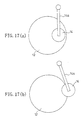
semiconductor substrate 13 is completed, the verticallymovable member 22 is moved downward relative to theplaten 11, as shown in FIG. 16(b). - Next, as shown in FIGS. 17(a) and 17(b), the
arm 14a of thesubstrate holding head 14 is rotated along the surface of thepolishing pad 12 so that a part of thesubstrate holding head 14 and therefore a part of thesemiconductor substrate 13 thrust out from thepolishing pad 12. Consequently, the adhesion of thepolishing pad 12 to thesemiconductor substrate 13 is reduced to permit easy removal of thesemiconductor substrate 13 from thepolishing pad 12. - FIGS. 18(a) and 18(b) show another structure in which the
substrate holding head 14 is moved along the surface of thepolishing pad 12. Thesubstrate holding head 14 is held by a horizontalmovable member 23 moving horizontally in parallel with the surface of thepolishing pad 12. - When the polishing of the
semiconductor substrate 13 is completed, the verticallymovable member 22 is moved downward relative to theplaten 11 as shown in FIG. 16(b) and then the horizontalmovable member 23 is moved horizontally as shown in FIGS. 18(a) and 18(b) to move thesubstrate holding head 14 along the surface of thepolishing pad 12. Consequently, a part of thesubstrate holding head 14 and therefore a part of thesemiconductor substrate 13 thrust out from thepolishing pad 12, so that thesemiconductor substrate 13 is removed easily from the top surface of thepolishing pad 12. - FIG. 19 schematically shows the plan configuration of a polishing apparatus according to a sixth embodiment of the present invention.
- As shown in FIG. 19, the sixth embodiment also comprises a
platen 11, apolishing pad 12, asubstrate holding head 14, and aslurry supply pipe 16, similarly to the first embodiment. Asemiconductor substrate 13 is rotated and pressed against thepolishing pad 12 on theplaten 11. Aslurry 15 is supplied in a prescribed amount from theslurry supply pipe 16 onto thepolishing pad 12. In FIG. 19, the drawing of a polishing-pad holder 11a of theplaten 11 is omitted. - The sixth embodiment is characterized in that a ring-shaped
rotary member 24 rotated in a plane vertical to the surface of thepolishing pad 12 by rotating means other than the rotating means for theplaten 11 is provided outside the polishing-pad holder 11a of theplaten 11. The drawing of a mechanism for rotating therotary member 24 is omitted here. On therotary member 24, a plurality of slat-likeslurry holding members 19 having the same configuration as in the fourth embodiment are provided as the slurry holding means along the outer circumferential surface of thepolishing pad 12 to hold theslurry 15 on thepolishing pad 12. Theslurry holding member 19 rotates relative to thepolishing pad 12 with the rotation of therotary member 24. Theslurry holding member 19 is held so that the top position thereof becomes higher in level than the surface of thepolishing pad 12 during polishing. - An
arm 14a of thesubstrate holding head 14 is provided to perform a rotary movement over the surface of thepolishing pad 12, similarly to the fifth embodiment. - The two-dimensional arrangement of the
slurry holding member 19 is the same as in the fourth embodiment so that theslurry 15 supplied from theslurry supply pipe 16 and directed to the peripheral portion of theplaten 11 by a centrifugal force accompanying the rotation of theplaten 11 changes its direction in collision with theslurry holding member 19 and is stored on thepolishing pad 12. As a result, theslurry 15 is evenly spread over thepolishing pad 12 before it is used in the polishing of thesemiconductor substrate 13. - Below, a polishing method using the polishing apparatus according to the sixth embodiment will be described with reference to FIGS. 19 and 20.
- Initially, as shown in FIG. 19, the
slurry 15 is supplied from theslurry supply pipe 16 onto a portion of thepolishing pad 12 corresponding to the near-central portion of theplaten 11, while theplaten 11 and thesubstrate holding head 14 are rotated individually. As a result, theslurry 15 flows toward the outside of thepolishing pad 12 due to the centrifugal force accompanying the rotation of theplaten 11 and is supplied to the interface between thesemiconductor substrate 13 and thepolishing pad 12. In this case, theslurry 15 on thepolishing pad 12 tends to flow to the outside of thepolishing pad 12 due to the centrifugal force accompanying the rotation of theplaten 11 but changes its direction in collision with theslurry holding member 19 and is stored on thepolishing pad 12. As a result, theslurry 15 is evenly spread over thepolishing pad 12 before it is used in the polishing of thesemiconductor substrate 13. - When the polishing of the
semiconductor substrate 13 is completed, therotary member 24 is rotated in a plane vertical to the surface of thepolishing pad 12, as shown in FIG. 20, and then thearm 14a of thesubstrate holding head 14 is rotated over the surface of thepolishing pad 12 so that a part of thesubstrate holding head 14 and therefore a part of thesemiconductor substrate 13 thrust out from thepolishing pad 12, similarly to the fifth embodiment. Consequently, the adhesion of thepolishing pad 12 to thesemiconductor substrate 13 is reduced to permit easy removal of thesemiconductor substrate 13 from thepolishing pad 12. - As shown in FIGS. 18(a) and 18(b), the
substrate holding head 14 may be held by a horizontalmovable member 23 moving horizontally in parallel with the surface of thepolishing pad 12 so that a part of thesubstrate holding head 14 and therefore a part of thesemiconductor substrate 13 thrust out from thepolishing pad 12. - FIG. 21 shows respective relationships between the amounts of supplied slurry and the polishing rates in the case where polishing is performed by using the polishing apparatus according to the individual embodiments of the present invention and in the case where polishing is performed by using the conventional polishing apparatus. Although the amount of supplied slurry required to maintain a sufficient polishing rate is L0 in the conventional embodiment, the present invention requires L1, which is smaller than L0, to maintain a polishing rate on the same order as in the conventional embodiment.
Claims (18)
- An apparatus for polishing a semiconductor substrate (13) comprising:wherein said slurry pushing plate (18) is a pushing plate (18) held over said polishing pad (12) to push, to the central portion of said platen (11), the slurry (15) brought in contact therewith by the centrifugal force accompanying the rotation of said platen (11);a platen (11) having a flat surface (11a) and rotating around a shaft (11b) vertical to said flat surface (11a);a polishing pad (12) disposed on said flat surface (11a) of said platen (11);slurry supplying means (16) for supplying a slurry (15) onto said polishing pad (12);substrate holding means (14) for holding a semiconductor substrate (13) and pressing it against said polishing pad (12); anda slurry pushing plate (18) for pushing, to a central portion of said platen (11), the slurry (15) supplied onto said polishing pad (12) and caused to flow to a peripheral portion of said platen (11) by a centrifugal force accompanying the rotation of said platen (11);
wherein:said pushing plate (18) is positioned to intersect a radial direction of the platen (11) such that an inner portion (18a) of said pushing plate (18) in the radial direction of the platen (11) is downstream of an outer portion (18b) of said pushing plate (18) in the radial direction of the platen (11) in the direction of rotation of the platen (11) during polishing. - An apparatus for polishing a semiconductor substrate according to claim 1, wherein said pushing plate (18) is provided rotatable in a direction opposite to the rotation of the platen (11) during polishing.
- An apparatus for polishing a semiconductor substrate (13) comprising:wherein said slurry pushing plate (18) is a pushing plate (18) held over said polishing pad (12) to push, to the central portion of said platen (11), the slurry (15) brought in contact therewith by the centrifugal force accompanying the rotation of said platen (11);a platen (11) having a flat surface (11a) and rotating around a shaft (11b) vertical to said flat surface (11a);a polishing pad (12) disposed on said flat surface (11a) of said platen (11);slurry supplying means (16) for supplying a slurry (15) onto said polishing pad (12);substrate holding means (14) for holding a semiconductor substrate (13) and pressing it against said polishing pad (12); anda slurry pushing plate (18) for pushing, to a central portion of said platen (11), the slurry (15) supplied onto said polishing pad (12) and caused to flow to a peripheral portion of said platen (11) by a centrifugal force accompanying the rotation of said platen (11);
whereina plurality of pushing plates (18) are spaced along the periphery of said platen (11). - An apparatus for polishing a semiconductor substrate (13) comprising:witha platen (11) having a flat surface (11a) and rotating around a shaft (11b) vertical to said flat surface (11a);a polishing pad (12) disposed on said flat surface (11a) of said platen (11);slurry supplying means (16) for supplying a slurry (15) onto said polishing pad (12);substrate holding means (14) for holding a semiconductor substrate (13) and pressing it against said polishing pad (12);slurry pushing means (17) for pushing, to a central portion of said platen (11), the slurry (15) supplied onto said polishing pad (12) and caused to flow to a peripheral portion of said platen (11) by a centrifugal force accompanying the rotation of said platen (11), wherein said slurry pushing means (17) has gas ejecting means (17a) for ejecting a gas for pushing the slurry (15) on said polishing pad (12) to a central portion of said platen (11).
- An apparatus for polishing a semiconductor substrate according to claim 4, wherein a plurality of gas ejecting means (17a) are provided along the periphery of said platen (11).
- An apparatus for polishing a semiconductor substrate (13) comprising:whereina platen (11) having a flat surface (11a) and rotating around a shaft (11b) vertical to said flat surface (11a);a polishing pad (12) disposed on said flat surface (11a) of said platen (11);slurry supplying means (16) for supplying a slurry (15) onto said polishing pad (12);substrate holding means (14) for holding a semiconductor substrate (13) and pressing it against said polishing pad (12);slurry pushing means (21) for pushing, to a central portion of said platen (11), the slurry (15) supplied onto said polishing pad (12) and caused to flow to a peripheral portion of said platen (11) by a centrifugal force accompanying the rotation of said platen (11), wherein said slurry pushing means (21) has a rotary member (21) provided in contact with or slightly spaced from a top surface of said polishing pad (12) and rotating in a direction opposite to the rotation of said platen (11)
said rotary member (21) has a projecting portion on the outer circumferential surface thereof. - An apparatus for polishing a semiconductor substrate (13) comprising:whereina platen (11) having a flat surface (11a) and rotating around a shaft (11b) vertical to said flat surface (11a);a polishing pad (12) disposed on said flat surface (11a) of said platen (11); slurry supplying means (16) for supplying a slurry (15) onto said polishing pad (12);substrate holding means (14) for holding a semiconductor substrate (13) and pressing it against said polishing pad (12); anda slurry holding member (19) provided on an edge portion of said platen (11)
said slurry holding member (19) is provided such that an inner portion of the slurry holding member (19) in a radial direction of the platen (11) is downstream of an outer portion of the slurry holding member (19) in the radial direction of the platen (11) in the direction of rotation of the platen (11) during polishing so as to hold the slurry (15) supplied onto said polishing pad (12) and caused to flow to a peripheral portion of said platen (11) by a centrifugal force accompanying the rotation of said platen (11) on said polishing pad (12). - An apparatus for polishing a semiconductor substrate according to claim 7, wherein a plurality of slurry holding members (19) are spaced along the periphery of said platen (11).
- An apparatus for polishing a semiconductor substrate according to claim 8, wherein, of said plurality of slurry holding members (19), adjacent ones are overlapping in the radial direction of the platen (11).
- An apparatus for polishing a semiconductor substrate according to claim 7, wherein said slurry holding member (19) is provided movable upwardly, downwardly, or outwardly from said polishing pad (12), and
said substrate holding member (14) is provided movable in a plane in parallel with said polishing pad (12) while holding said semiconductor substrate (13). - A method of polishing a semiconductor substrate, comprising:wherein said pushing plate (18) is held over said polishing pad (12); whereina slurry supplying step of supplying a slurry (15) onto a polishing pad (12) disposed on a flat surface (11a) of a platen (11) rotating around a shaft (11b) vertical to said flat surface (11a);a substrate polishing step of polishing a semiconductor substrate (13) by pressing it against said polishing pad (12);a slurry pushing step of pushing, to a central portion of said platen (11), the slurry (15) supplied onto said polishing pad (12) and caused to flow to a peripheral portion of said platen (11) by a centrifugal force accompanying the rotation of said platen (11), wherein said slurry pushing step includes a step of pushing the slurry (15) on said polishing pad (12) to the central portion of said platen (11) by means of a pushing plate (18);
said slurry pushing step includes a step of pushing the slurry (15) on said polishing pad (12) to the central portion of said platen (11) by means of said pushing plate (18) positioned to intersect a radial direction of the platen such that an inner portion (18a) of the pushing plate (18) in the radial direction of the platen (11) is downstream of an outer portion (18b) of the pushing plate (18) in the radial direction of the platen (11) in the direction of rotation of the platen (11) during polishing. - A method of polishing a semiconductor substrate, comprising:wherein said pushing plate (18) is held over said polishing pad (12); whereina slurry supplying step of supplying a slurry (15) onto a polishing pad (12) disposed on a flat surface (11a) of a platen (11) rotating around a shaft (11b) vertical to said flat surface (11a);a substrate polishing step of polishing a semiconductor substrate (13) by pressing it against said polishing pad (12);a slurry pushing step of pushing, to a central portion of said platen (11), the slurry (15) supplied onto said polishing pad (12) and caused to flow to a peripheral portion of said platen (11) by a centrifugal force accompanying the rotation of said platen (11), wherein said slurry pushing step includes a step of pushing the slurry (15) on said polishing pad (12) to the central portion of said platen (11) by means of a pushing plate (18);
the method further comprises a cleaning-liquid removing step of removing a cleaning liquid supplied onto said polishing pad (12) by rotating said platen (11) in a direction opposite to the rotation of the platen (11) during polishing. - A method of polishing a semiconductor substrate, comprising:wherein there is furthera slurry supplying step of supplying a slurry (15) onto a polishing pad (12) disposed on a flat surface (11a) of a platen (11) rotating around a shaft vertical (11b) to said flat surface (11a);a substrate polishing step of polishing a semiconductor substrate (13) the slurry (15) supplied onto said polishing pad (12)a slurry pushing step of pushing, to a central portion of said platen (11), the slurry (15) supplied onto said polishing pad (12) and caused to flow to a peripheral portion of said platen (11) by a centrifugal force accompanying the rotation of said platen (11), wherein said slurry pushing step includes a step of ejecting a gas toward a central portion of said platen (11) to push the slurry (15) on said polishing pad (12) to the central portion of said platen (11).
- A method of polishing a semiconductor substrate, comprising:whereina slurry supplying step of supplying a slurry (15) onto a polishing pad (12) disposed on a flat surface (11a) of a platen (11) rotating around a shaft (11b) vertical to said flat surface (11a);a substrate polishing step of polishing a semiconductor substrate (13) by pressing it against said polishing pad (12); anda slurry holding step of holding the slurry (15) supplied onto said polishing pad (12) and caused to flow to a peripheral portion of said platen (11) by a centrifugal force accompanying the rotation of said platen (11) on said polishing pad,
the slurry holding step is performed by means of a slurry holding member (19) fixed to an edge portion of said platen (11) such that an inner portion of the slurry holding member (19) in a radial direction of the platen (11) is downstream of an outer portion of the slurry holding member (19) in the radial direction of the platen (11) in the direction of rotation of the platen (11) during polishing. - A method of polishing a semiconductor substrate according to claim 14,
wherein said slurry holding step includes a step of holding the slurry (15) on said polishing pad (12) by means of a plurality of slurry holding members (19) spaced along the periphery of said platen. - A method of polishing a semiconductor substrate according to claim 15, wherein said slurry holding step includes a step of holding the slurry (15) on said polishing pad (12) by means of said plurality of slurry holding members (19) of which adjacent ones are overlapping in the radial direction of the platen (11).
- A method of polishing a semiconductor substrate according to claim 14, further comprising a cleaning-liquid removing step of removing a cleaning liquid supplied onto said polishing pad (12) by rotating said platen (11) in a direction opposite to the rotation of the platen (11) during polishing.
- A method of polishing a semiconductor substrate according to claim 14, further comprising:a slurry-holding-member moving step of moving said slurry holding member (19) upwardly, downwardly, or outwardly from said polishing pad (12); anda substrate moving step of moving said semiconductor substrate (13) in a plane in parallel with said polishing pad (12) such that at least a part of said semiconductor substrate (13) thrusts out from said polishing pad (12).
Applications Claiming Priority (3)
| Application Number | Priority Date | Filing Date | Title |
|---|---|---|---|
| JP23135595 | 1995-09-08 | ||
| JP231355/95 | 1995-09-08 | ||
| JP23135595 | 1995-09-08 |
Publications (2)
| Publication Number | Publication Date |
|---|---|
| EP0763402A1 EP0763402A1 (en) | 1997-03-19 |
| EP0763402B1 true EP0763402B1 (en) | 2002-01-30 |
Family
ID=16922329
Family Applications (1)
| Application Number | Title | Priority Date | Filing Date |
|---|---|---|---|
| EP96113864A Expired - Lifetime EP0763402B1 (en) | 1995-09-08 | 1996-08-29 | Method and apparatus for polishing semiconductor substrate |
Country Status (4)
| Country | Link |
|---|---|
| US (1) | US5866480A (en) |
| EP (1) | EP0763402B1 (en) |
| KR (1) | KR970018240A (en) |
| DE (1) | DE69618882T2 (en) |
Families Citing this family (19)
| Publication number | Priority date | Publication date | Assignee | Title |
|---|---|---|---|---|
| JP2833552B2 (en) * | 1995-10-19 | 1998-12-09 | 日本電気株式会社 | Wafer polishing method and polishing apparatus |
| JPH10329011A (en) * | 1997-03-21 | 1998-12-15 | Canon Inc | Precise polishing device and method |
| US5921849A (en) * | 1997-06-04 | 1999-07-13 | Speedfam Corporation | Method and apparatus for distributing a polishing agent onto a polishing element |
| JP2000216120A (en) * | 1999-01-27 | 2000-08-04 | Mitsubishi Electric Corp | Polisher and manufacturing semiconductor device using the same |
| US6429131B2 (en) * | 1999-03-18 | 2002-08-06 | Infineon Technologies Ag | CMP uniformity |
| JP2001138233A (en) * | 1999-11-19 | 2001-05-22 | Sony Corp | Grinding apparatus, grinding method and cleaning method of grinding tool |
| US6887132B2 (en) * | 2001-09-10 | 2005-05-03 | Multi Planar Technologies Incorporated | Slurry distributor for chemical mechanical polishing apparatus and method of using the same |
| JP4101609B2 (en) * | 2001-12-07 | 2008-06-18 | 大日本スクリーン製造株式会社 | Substrate processing method |
| JP2003324085A (en) * | 2002-05-01 | 2003-11-14 | Mitsubishi Electric Corp | Device and method for polishing semiconductor wafer |
| US7128803B2 (en) * | 2002-06-28 | 2006-10-31 | Lam Research Corporation | Integration of sensor based metrology into semiconductor processing tools |
| US7309618B2 (en) | 2002-06-28 | 2007-12-18 | Lam Research Corporation | Method and apparatus for real time metal film thickness measurement |
| JP2005271151A (en) * | 2004-03-25 | 2005-10-06 | Toshiba Corp | Polishing apparatus and polishing method |
| JP5298383B2 (en) * | 2007-04-25 | 2013-09-25 | Esファイバービジョンズ株式会社 | Heat-adhesive conjugate fiber excellent in bulkiness and flexibility and fiber molded article using the same |
| KR101110268B1 (en) * | 2010-04-30 | 2012-02-16 | 삼성전자주식회사 | Chemical mechanical polishing system which prevents air pressure tube electric wires from being twisted |
| TWI517935B (en) * | 2013-04-16 | 2016-01-21 | 國立台灣科技大學 | Supplying system of adding gas into slurry and method thereof |
| JP6975078B2 (en) | 2018-03-15 | 2021-12-01 | キオクシア株式会社 | Semiconductor manufacturing equipment and methods for manufacturing semiconductor equipment |
| JP7162465B2 (en) | 2018-08-06 | 2022-10-28 | 株式会社荏原製作所 | Polishing device and polishing method |
| JP7083722B2 (en) | 2018-08-06 | 2022-06-13 | 株式会社荏原製作所 | Polishing equipment and polishing method |
| CN111113224B (en) * | 2019-12-27 | 2020-11-27 | 绍兴圣万特热流道有限公司 | Automatic machining equipment for hot runner mold |
Citations (1)
| Publication number | Priority date | Publication date | Assignee | Title |
|---|---|---|---|---|
| EP0763401A1 (en) * | 1995-08-24 | 1997-03-19 | Matsushita Electric Industrial Co., Ltd. | Method and apparatus for polishing semiconductor substrate |
Family Cites Families (8)
| Publication number | Priority date | Publication date | Assignee | Title |
|---|---|---|---|---|
| US4910155A (en) * | 1988-10-28 | 1990-03-20 | International Business Machines Corporation | Wafer flood polishing |
| US5081051A (en) * | 1990-09-12 | 1992-01-14 | Intel Corporation | Method for conditioning the surface of a polishing pad |
| US5308438A (en) * | 1992-01-30 | 1994-05-03 | International Business Machines Corporation | Endpoint detection apparatus and method for chemical/mechanical polishing |
| US5216843A (en) * | 1992-09-24 | 1993-06-08 | Intel Corporation | Polishing pad conditioning apparatus for wafer planarization process |
| US5341602A (en) * | 1993-04-14 | 1994-08-30 | Williams International Corporation | Apparatus for improved slurry polishing |
| JP2903980B2 (en) * | 1993-11-30 | 1999-06-14 | 信越半導体株式会社 | Wafer polishing method and apparatus |
| US5650039A (en) * | 1994-03-02 | 1997-07-22 | Applied Materials, Inc. | Chemical mechanical polishing apparatus with improved slurry distribution |
| US5527424A (en) * | 1995-01-30 | 1996-06-18 | Motorola, Inc. | Preconditioner for a polishing pad and method for using the same |
-
1996
- 1996-08-20 KR KR1019960034339A patent/KR970018240A/en not_active Application Discontinuation
- 1996-08-26 US US08/697,509 patent/US5866480A/en not_active Expired - Lifetime
- 1996-08-29 DE DE69618882T patent/DE69618882T2/en not_active Expired - Lifetime
- 1996-08-29 EP EP96113864A patent/EP0763402B1/en not_active Expired - Lifetime
Patent Citations (1)
| Publication number | Priority date | Publication date | Assignee | Title |
|---|---|---|---|---|
| EP0763401A1 (en) * | 1995-08-24 | 1997-03-19 | Matsushita Electric Industrial Co., Ltd. | Method and apparatus for polishing semiconductor substrate |
Also Published As
| Publication number | Publication date |
|---|---|
| US5866480A (en) | 1999-02-02 |
| DE69618882T2 (en) | 2002-07-11 |
| EP0763402A1 (en) | 1997-03-19 |
| DE69618882D1 (en) | 2002-03-14 |
| KR970018240A (en) | 1997-04-30 |
Similar Documents
| Publication | Publication Date | Title |
|---|---|---|
| EP0763402B1 (en) | Method and apparatus for polishing semiconductor substrate | |
| US5769697A (en) | Method and apparatus for polishing semiconductor substrate | |
| US20020068516A1 (en) | Apparatus and method for controlled delivery of slurry to a region of a polishing device | |
| US7708622B2 (en) | Apparatuses and methods for conditioning polishing pads used in polishing micro-device workpieces | |
| EP0764478A1 (en) | Method of and apparatus for cleaning workpiece | |
| US6364752B1 (en) | Method and apparatus for dressing polishing cloth | |
| US9375825B2 (en) | Polishing pad conditioning system including suction | |
| JP2001018169A (en) | Polishing device | |
| US6409579B1 (en) | Method and apparatus for conditioning a polish pad at the point of polish and for dispensing slurry at the point of polish | |
| WO2001027350A1 (en) | Optimal offset, pad size and pad shape for cmp buffing and polishing | |
| US6343977B1 (en) | Multi-zone conditioner for chemical mechanical polishing system | |
| US10974366B2 (en) | Conditioning wheel for polishing pads | |
| US6813796B2 (en) | Apparatus and methods to clean copper contamination on wafer edge | |
| US6793565B1 (en) | Orbiting indexable belt polishing station for chemical mechanical polishing | |
| US11890717B2 (en) | Polishing system with platen for substrate edge control | |
| JP2983905B2 (en) | Method and apparatus for polishing semiconductor substrate | |
| JP3326841B2 (en) | Polishing equipment | |
| WO2004059714A1 (en) | Polishing device and method of producing semiconductor device | |
| JPH10309661A (en) | Method and device for polishing semiconductor substrate | |
| JP3692970B2 (en) | Polishing pad | |
| WO1998012020A1 (en) | Methods and apparatus for uniform polishing of a workpiece | |
| CN110744444B (en) | Polishing pad and polishing apparatus | |
| JP2002178260A (en) | Polishing device | |
| JP3646430B2 (en) | Chemical mechanical polishing method and chemical mechanical polishing apparatus | |
| CN117295585A (en) | Chemical mechanical polishing with die-based modification |
Legal Events
| Date | Code | Title | Description |
|---|---|---|---|
| PUAI | Public reference made under article 153(3) epc to a published international application that has entered the european phase |
Free format text: ORIGINAL CODE: 0009012 |
|
| AK | Designated contracting states |
Kind code of ref document: A1 Designated state(s): DE FR GB |
|
| 17P | Request for examination filed |
Effective date: 19970320 |
|
| 17Q | First examination report despatched |
Effective date: 19991026 |
|
| GRAG | Despatch of communication of intention to grant |
Free format text: ORIGINAL CODE: EPIDOS AGRA |
|
| GRAG | Despatch of communication of intention to grant |
Free format text: ORIGINAL CODE: EPIDOS AGRA |
|
| GRAH | Despatch of communication of intention to grant a patent |
Free format text: ORIGINAL CODE: EPIDOS IGRA |
|
| GRAH | Despatch of communication of intention to grant a patent |
Free format text: ORIGINAL CODE: EPIDOS IGRA |
|
| GRAA | (expected) grant |
Free format text: ORIGINAL CODE: 0009210 |
|
| REG | Reference to a national code |
Ref country code: GB Ref legal event code: IF02 |
|
| AK | Designated contracting states |
Kind code of ref document: B1 Designated state(s): DE FR GB |
|
| REF | Corresponds to: |
Ref document number: 69618882 Country of ref document: DE Date of ref document: 20020314 |
|
| ET | Fr: translation filed | ||
| PLBE | No opposition filed within time limit |
Free format text: ORIGINAL CODE: 0009261 |
|
| STAA | Information on the status of an ep patent application or granted ep patent |
Free format text: STATUS: NO OPPOSITION FILED WITHIN TIME LIMIT |
|
| 26N | No opposition filed | ||
| PGFP | Annual fee paid to national office [announced via postgrant information from national office to epo] |
Ref country code: FR Payment date: 20090814 Year of fee payment: 14 |
|
| PGFP | Annual fee paid to national office [announced via postgrant information from national office to epo] |
Ref country code: GB Payment date: 20090826 Year of fee payment: 14 Ref country code: DE Payment date: 20090827 Year of fee payment: 14 |
|
| GBPC | Gb: european patent ceased through non-payment of renewal fee |
Effective date: 20100829 |
|
| REG | Reference to a national code |
Ref country code: FR Ref legal event code: ST Effective date: 20110502 |
|
| REG | Reference to a national code |
Ref country code: DE Ref legal event code: R119 Ref document number: 69618882 Country of ref document: DE Effective date: 20110301 |
|
| PG25 | Lapsed in a contracting state [announced via postgrant information from national office to epo] |
Ref country code: DE Free format text: LAPSE BECAUSE OF NON-PAYMENT OF DUE FEES Effective date: 20110301 Ref country code: FR Free format text: LAPSE BECAUSE OF NON-PAYMENT OF DUE FEES Effective date: 20100831 |
|
| PG25 | Lapsed in a contracting state [announced via postgrant information from national office to epo] |
Ref country code: GB Free format text: LAPSE BECAUSE OF NON-PAYMENT OF DUE FEES Effective date: 20100829 |