EP0757429B1 - Switched mode power supply with power factor correction - Google Patents
Switched mode power supply with power factor correction Download PDFInfo
- Publication number
- EP0757429B1 EP0757429B1 EP95410076A EP95410076A EP0757429B1 EP 0757429 B1 EP0757429 B1 EP 0757429B1 EP 95410076 A EP95410076 A EP 95410076A EP 95410076 A EP95410076 A EP 95410076A EP 0757429 B1 EP0757429 B1 EP 0757429B1
- Authority
- EP
- European Patent Office
- Prior art keywords
- output
- switching device
- voltage
- inductor
- power supply
- Prior art date
- Legal status (The legal status is an assumption and is not a legal conclusion. Google has not performed a legal analysis and makes no representation as to the accuracy of the status listed.)
- Expired - Lifetime
Links
- 238000012937 correction Methods 0.000 title abstract description 12
- 238000004804 winding Methods 0.000 claims abstract description 42
- 239000003990 capacitor Substances 0.000 claims abstract description 41
- 230000001105 regulatory effect Effects 0.000 claims abstract description 14
- 230000001276 controlling effect Effects 0.000 claims abstract description 6
- 230000001419 dependent effect Effects 0.000 claims abstract description 6
- 230000008878 coupling Effects 0.000 claims abstract description 5
- 238000010168 coupling process Methods 0.000 claims abstract description 5
- 238000005859 coupling reaction Methods 0.000 claims abstract description 5
- 125000004122 cyclic group Chemical group 0.000 claims abstract description 5
- 230000004907 flux Effects 0.000 claims description 17
- 230000008859 change Effects 0.000 claims description 8
- 230000001052 transient effect Effects 0.000 claims description 8
- 238000012544 monitoring process Methods 0.000 claims description 4
- 238000007599 discharging Methods 0.000 claims 2
- 230000000977 initiatory effect Effects 0.000 claims 2
- 230000001939 inductive effect Effects 0.000 description 8
- 230000007423 decrease Effects 0.000 description 6
- 238000010586 diagram Methods 0.000 description 6
- 238000002955 isolation Methods 0.000 description 4
- 238000013459 approach Methods 0.000 description 3
- 238000013461 design Methods 0.000 description 3
- 230000000694 effects Effects 0.000 description 3
- 238000001514 detection method Methods 0.000 description 2
- 238000000034 method Methods 0.000 description 2
- 230000004044 response Effects 0.000 description 2
- 230000002441 reversible effect Effects 0.000 description 2
- UXUFTKZYJYGMGO-CMCWBKRRSA-N (2s,3s,4r,5r)-5-[6-amino-2-[2-[4-[3-(2-aminoethylamino)-3-oxopropyl]phenyl]ethylamino]purin-9-yl]-n-ethyl-3,4-dihydroxyoxolane-2-carboxamide Chemical compound O[C@@H]1[C@H](O)[C@@H](C(=O)NCC)O[C@H]1N1C2=NC(NCCC=3C=CC(CCC(=O)NCCN)=CC=3)=NC(N)=C2N=C1 UXUFTKZYJYGMGO-CMCWBKRRSA-N 0.000 description 1
- 230000003247 decreasing effect Effects 0.000 description 1
- 238000009499 grossing Methods 0.000 description 1
- 230000003993 interaction Effects 0.000 description 1
- 238000012986 modification Methods 0.000 description 1
- 230000004048 modification Effects 0.000 description 1
- 230000009467 reduction Effects 0.000 description 1
- 230000004043 responsiveness Effects 0.000 description 1
- 230000001360 synchronised effect Effects 0.000 description 1
Images


Classifications
-
- H—ELECTRICITY
- H02—GENERATION; CONVERSION OR DISTRIBUTION OF ELECTRIC POWER
- H02M—APPARATUS FOR CONVERSION BETWEEN AC AND AC, BETWEEN AC AND DC, OR BETWEEN DC AND DC, AND FOR USE WITH MAINS OR SIMILAR POWER SUPPLY SYSTEMS; CONVERSION OF DC OR AC INPUT POWER INTO SURGE OUTPUT POWER; CONTROL OR REGULATION THEREOF
- H02M1/00—Details of apparatus for conversion
- H02M1/42—Circuits or arrangements for compensating for or adjusting power factor in converters or inverters
- H02M1/4208—Arrangements for improving power factor of AC input
- H02M1/4258—Arrangements for improving power factor of AC input using a single converter stage both for correction of AC input power factor and generation of a regulated and galvanically isolated DC output voltage
-
- G—PHYSICS
- G06—COMPUTING; CALCULATING OR COUNTING
- G06F—ELECTRIC DIGITAL DATA PROCESSING
- G06F1/00—Details not covered by groups G06F3/00 - G06F13/00 and G06F21/00
- G06F1/26—Power supply means, e.g. regulation thereof
- G06F1/28—Supervision thereof, e.g. detecting power-supply failure by out of limits supervision
-
- H—ELECTRICITY
- H02—GENERATION; CONVERSION OR DISTRIBUTION OF ELECTRIC POWER
- H02M—APPARATUS FOR CONVERSION BETWEEN AC AND AC, BETWEEN AC AND DC, OR BETWEEN DC AND DC, AND FOR USE WITH MAINS OR SIMILAR POWER SUPPLY SYSTEMS; CONVERSION OF DC OR AC INPUT POWER INTO SURGE OUTPUT POWER; CONTROL OR REGULATION THEREOF
- H02M3/00—Conversion of dc power input into dc power output
- H02M3/005—Conversion of dc power input into dc power output using Cuk converters
-
- H—ELECTRICITY
- H02—GENERATION; CONVERSION OR DISTRIBUTION OF ELECTRIC POWER
- H02M—APPARATUS FOR CONVERSION BETWEEN AC AND AC, BETWEEN AC AND DC, OR BETWEEN DC AND DC, AND FOR USE WITH MAINS OR SIMILAR POWER SUPPLY SYSTEMS; CONVERSION OF DC OR AC INPUT POWER INTO SURGE OUTPUT POWER; CONTROL OR REGULATION THEREOF
- H02M3/00—Conversion of dc power input into dc power output
- H02M3/22—Conversion of dc power input into dc power output with intermediate conversion into ac
- H02M3/24—Conversion of dc power input into dc power output with intermediate conversion into ac by static converters
- H02M3/28—Conversion of dc power input into dc power output with intermediate conversion into ac by static converters using discharge tubes with control electrode or semiconductor devices with control electrode to produce the intermediate ac
- H02M3/325—Conversion of dc power input into dc power output with intermediate conversion into ac by static converters using discharge tubes with control electrode or semiconductor devices with control electrode to produce the intermediate ac using devices of a triode or a transistor type requiring continuous application of a control signal
- H02M3/335—Conversion of dc power input into dc power output with intermediate conversion into ac by static converters using discharge tubes with control electrode or semiconductor devices with control electrode to produce the intermediate ac using devices of a triode or a transistor type requiring continuous application of a control signal using semiconductor devices only
- H02M3/33507—Conversion of dc power input into dc power output with intermediate conversion into ac by static converters using discharge tubes with control electrode or semiconductor devices with control electrode to produce the intermediate ac using devices of a triode or a transistor type requiring continuous application of a control signal using semiconductor devices only with automatic control of the output voltage or current, e.g. flyback converters
-
- Y—GENERAL TAGGING OF NEW TECHNOLOGICAL DEVELOPMENTS; GENERAL TAGGING OF CROSS-SECTIONAL TECHNOLOGIES SPANNING OVER SEVERAL SECTIONS OF THE IPC; TECHNICAL SUBJECTS COVERED BY FORMER USPC CROSS-REFERENCE ART COLLECTIONS [XRACs] AND DIGESTS
- Y02—TECHNOLOGIES OR APPLICATIONS FOR MITIGATION OR ADAPTATION AGAINST CLIMATE CHANGE
- Y02B—CLIMATE CHANGE MITIGATION TECHNOLOGIES RELATED TO BUILDINGS, e.g. HOUSING, HOUSE APPLIANCES OR RELATED END-USER APPLICATIONS
- Y02B70/00—Technologies for an efficient end-user side electric power management and consumption
- Y02B70/10—Technologies improving the efficiency by using switched-mode power supplies [SMPS], i.e. efficient power electronics conversion e.g. power factor correction or reduction of losses in power supplies or efficient standby modes
-
- Y—GENERAL TAGGING OF NEW TECHNOLOGICAL DEVELOPMENTS; GENERAL TAGGING OF CROSS-SECTIONAL TECHNOLOGIES SPANNING OVER SEVERAL SECTIONS OF THE IPC; TECHNICAL SUBJECTS COVERED BY FORMER USPC CROSS-REFERENCE ART COLLECTIONS [XRACs] AND DIGESTS
- Y02—TECHNOLOGIES OR APPLICATIONS FOR MITIGATION OR ADAPTATION AGAINST CLIMATE CHANGE
- Y02P—CLIMATE CHANGE MITIGATION TECHNOLOGIES IN THE PRODUCTION OR PROCESSING OF GOODS
- Y02P80/00—Climate change mitigation technologies for sector-wide applications
- Y02P80/10—Efficient use of energy, e.g. using compressed air or pressurized fluid as energy carrier
Definitions
- the present invention relates to a switched mode power supply with power factor correction.
- Switched mode power supplies are frequently used in electronic equipment for producing a regulated dc output from an ac mains input.
- a switched mode power supply for such an application typically comprises a rectifier unit for producing a rectified and at least partially smoothed dc output, and a DC/DC converter such as a flyback or forward converter coupled to the rectifier unit.
- the DC/DC converter normally serves not only to produce a regulated dc output but also to provide isolation of the output from the ac mains input.
- a switched mode power supply of the above form will generally exhibit a poor (low) power factor, this latter being the ratio of the true power drawn by the power supply to the product of the RMS values of the actual voltage and current.
- the discrepancy between the two values is due to the harmonic distortion of the rectifier unit and the smoothing capacitors.
- One known approach to providing power factor correction in switched mode power supplies is to dispense with the large capacitors generally provided in the rectifier unit and then seek to cause the current drawn during each switching cycle of the downstream converter to be proportional to the instantaneous value of the rectified half sine wave input voltage (the switching frequency being much higher than the mains frequency).
- the converter By arranging for the current drawn by the converter to be proportional to the input voltage, the converter (and thus the switched mode power supply) appears resistive in nature with a high power factor.
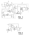
- the switched mode power supply shown in Figure 1 comprises a bridge rectifier 11 feeding a boost regulator 12 which, in turn, supplies a flyback converter 13.
- the boost regulator 12 stores energy in a reservoir capacitor 14 at a voltage above the maximum of the rectified output from the bridge rectifier 11, and the flyback converter 13 then runs off the energy source constituted by the capacitor 14.
- the boost regulator 12 is arranged to charge the capacitor 14 with a current proportional to the rectified voltage V IN produced at the output of the bridge 11 whereby to present itself as a resistive load to the ac mains.
- the duty cycle of the switching device (MOSFET) 16 of the regulator 12 is controlled by a fixed-frequency pulse width modulation (PWM) control block 17 that is responsive to the instantaneaous value of V IN (as sensed via a potential divider network 18) to increase the on time of the switching device 16 in proportion to the sensed value of V IN .
- PWM pulse width modulation
- the natural characteristics of the boost regulator are such that when operated in a continuous mode, the average input current will be proportional to the on time of the duty cycle of the switching device 16 provided that the voltage V C is constant; this latter may be assumed to be the case on the time scale of the ac mains frequency in view of the magnitude of the capacitor 14.
- V C the voltage of the switching device 16
- low pass filter 15 ensures that this adjustment is on a longer timescale to that of the variation in voltage V IN . Since the input signal of the PWM control block 17 must still have the same shape as the converter input voltage as sensed by the divider network 18, the output of the low pass filter 15 is multiplied by the sensed input voltage in multiplier 24 before being fed to the PWM control block 17.
- the flyback converter 13 is of standard form and includes a pulse width modulation (PWM) control block 20 responsive to the value of the output voltage V O of the converter 13 to regulate the duty cycle of the converter switching device (MOSFET) 21 whereby to maintain the output voltage V O at a desired level (the loopback electronics, including a reference for setting the desired output voltage level, are incorporated in the control block 20).
- PWM pulse width modulation
- MOSFET converter switching device
- the transformer 22 of the flyback converter provides the isolation between the ac mains input "AC IN" and the output voltage V O .
- SEPIC Single Ended Primary Inductance Converter
- the SEPIC converter comprises a first energy-storing inductor 26 connected in series with a switching device 27 across the input to the regulator, and a second energy-storing inductor 28 connected in series with a capacitor 29 across the switching device 27.
- a diode 30 connects the junction of the second inductor 28 and capacitor 29 with an output reservoir capacitor 31 and load 32.
- the switching device 27 is controlled by a fixed-frequency PWM controller 33 responsive to the value of the output voltage V O to adjust the duty cycle of the device 27 such as to maintain V O constant.
- the values of both capacitors 29 and 31 are sufficiently large that the ripple across them at the switching frequency of the device 27 is small and may be ignored; the voltage across capacitor 29 is equal to the input voltage V IN .
- the most commonly used mode is one in which current flows continuously through both inductors 26 and 28.
- diode 30 is cut off and the load is supplied from capacitor 31; current I 1 builds through inductor 26 storing energy in it and similarly current I 2 builds up through the inductor 28 storing energy in this inductor.
- switching device 27 is off, the diode 30 conducts and energy is transferred from inductors 26 and 28 to the capacitor 31 and the load, the currents I 1 and I 2 through these inductors falling progressively. The switching device is then turned on again and the cycle of operation recommenced.
- a power supply comprising a rectifier arrangement for receiving an ac input and producing a rectified output at an output of the rectifier arrangement, and a flyback converter comprising an input circuit connected to the output of the rectifier arrangement, an output circuit for providing a regulated dc output voltage, and an energy-storing transformer that has primary and secondary windings respectively connected into said input and output circuits; the input circuit comprising:
- the input current is made proportional to the input voltage, thereby giving the desired resistive behaviour.
- the inductance values of the inductor and the transformer primary winding are equal; said predetermined turn-on condition being reached when the stored energy levels in the inductor and transformer are zero.
- the inductance value of the inductor is greater than that of the transformer primary winding; in this case, the transformer, following turn off of the switching device, first discharges to zero and is then recharged by the inductor until said predetermined turn-on condition is reached. It is also possible to arrange for the inductor to have a lesser inductance than the transformer primary winding.
- Detection of the predetermined turn-on condition can be effected in a number of ways because at this point, the flux in the transformer, and also in the inductor, ceases to change and the secondary current becomes zero. Of course, if the flux in the transformer or inductor ceases to change, the induced voltage in these components will become zero which is readily detected.
- the transformer is provided with a sensing winding and the voltage induced in this winding is then monitored to determine when the turn-on condition has been reached. An alternative would be to monitor the current in the transformer secondary winding.
- the on-time duration control means preferably comprises an output-voltage feedback loop including a low-pass filter for reducing a mains-related ripple component. Because this has the effect of reducing the responsiveness of the converter to load changes, a transient accelerator is advantageously included in the feedback loop, this transient accelerator being responsive to rapid changes and/or large deviations in said output voltage to bypass the low-pass filter and introduce these changes more quickly into said feedback signal.
- the feedback loop further comprises a minimum peak detector for detecting minimums in the voltage across the secondary winding of the transformer on the timescale of the mains frequency, the minimum voltage detector producing an output scaled and phase aligned with the output of the low-pass filter such as to act to cancel any residual ripple component in the latter.
- a power supply comprising a rectifier arrangement for receiving an ac input and producing a rectified output at an output of the rectifier arrangement, and a regulator connected to the output of the rectifier arrangement and operative to provide a regulated dc output voltage; said regulator comprising:
- FIG. 3 shows a first switched mode power supply providing power factor correction in accordance with the present invention.
- This power supply comprises a bridge rectifier 39 connected on its ac side to an ac mains supply (typically at 50 Hz).
- the dc side of the bridge rectifier supplies a double rectified sine wave input voltage V IN to a modified form of flyback converter that provides a regulated output of voltage V O .
- the modified flyback converter in turn comprises an input circuit 40 coupled to an output circuit 41 through an energy storing transformer 42.
- the input circuit 40 is similar in form to the front end of a SEPIC regulator (see Figure 2) and comprises an energy-storing inductor 43 connected in series with a switching device 44 across the output of the bridge rectifier 39, and a capacitor 45 connected in series with a primary winding 46 of the transformer 42 across the switching device 44.
- the inductance of inductor 43 is assumed to be the same as the inductance exhibited by the primary winding 46 with the secondary winding open (references below to the inductance of the transformer are to be understood as this inductance). Whilst it is preferred to have the inductance values of the inductor 43 and transformer 42 the same, this is not essential as will be explained later.
- the value of the capacitor 45 is such that it offers a high impedance at the ac mains frequency so as to block the passage of mains ripple, but a low impedance at the switching frequencies of the switching device 43.
- the output circuit 41 is of standard form for a flyback converter and comprises a secondary winding 47 feeding a reservoir capacitor 49 through a diode 48, the output voltage V O being developed across the capacitor 49 for supplying a load 50.
- the winding ration between the primary and secondary windings 46 and 47 is taken to be unity in the following description; in practice, this will generally not be the case, but the operating principles described below are not thereby affected.
- the switching device 44 (here shown as a MOSFET by way of example only) is cyclically turned on and off by control circuitry comprising elements 60 to 71 to be described in more detail hereinafter.
- control circuitry comprising elements 60 to 71 to be described in more detail hereinafter.
- this circuitry includes an on-time control block 65 which controls:
- Figure 4 shows the main components of the Figure 3 converter (excepting the control circuitry) and indicates the main voltages and currents of interest.
- I 1 the input current that flows through inductor 43
- V 1 the voltage at the junction of the inductor 43 and switching device 44
- V gs the voltage applied to the gate of the MOSFET constituting the switching device
- V gs the voltage across, and current through, the primary winding 46
- I 3 the current through the secondary winding 47
- the flux in transformer 42 is designeted ⁇ T .
- FIG. 5 shows the time plots of V gs , V 1 , I 1 , V 2 , I 2 , I 3 , and ⁇ T over four switching cycles of the switching device 44.
- Each switching cycle comprises a first period t ON when the device 44 is on (V gs high) and a second period t OFF when the device is off (V gs low).
- the input voltage V IN is assumed constant (which is reasonable since even though the input voltage varies sinusoidally, it does so at a much lower frequency that the switching frequencies of the switching device 44);
- the output voltage V O is also assumed constant over the illustrated four cycle period.
- the switching frequency of the device 44 may also be taken as constant over the illustrated four cycle period and, indeed, each illustrated cycle of operation is substantially identical.
- the voltage across the capacitor 45 will be substantially constant and equal to the input voltage V IN .
- the voltage V 2 will therefore be -V IN and both the inductor 43 and primary winding 46 will have the same driving voltage V IN thereacross causing the current through each (I 1 , I 2 respectively) to increase at the same rate, their inductances being the same. Energy is thus stored into the inductor 43 and transformer 42.
- the current I 3 is zero during the period t ON as the diode 48 is reverse biased and the load 50 is powered by current drawn from the reservoir capacitor 49.
- I 3 (which can now flow due to the forward biasing of diode 48) takes on an appropriate value; for the present case of a winding ratio of unity between the primary and secondary windings, the current I 3 will take on a value at the start of the period t OFF which is equal to twice the value of I 2 at the moment the switching device is turned off.
- the rate at which I 3 decreases (and thus also I 2 and I 1 ) will depend on the output voltage V O .
- the voltage V 1 on turn off of the switching device, the voltage V 1 will immediately rise to a level above V IN determined by the rate of decrease of current I 1 ; voltage V 2 will also rise by the same amount as V 1 .
- the rate of decrease of flux in the inductor 43 (this flux being a measure of stored energy) is, of course, of the same form as the current I 1 .
- the rate of decrease of flux ⁇ T in the transformer 42 is dependent on the rate of decrease of the currents I 2 and I 3 , as is illustrated in Figure 5.
- the flux of the inductor and transformer decrease at the same rate from the same starting value existing at the beginning of the period t OFF .
- the switching device 44 is left off, since neither the inductor nor the transformer has any stored energy and since the voltage across capacitor 45 balances the input voltage V IN , the currents I 1 , I 2 and I 3 would remain at zero with the fluxes in the inductor and transformer remaining constant at zero. In fact, in the present converter, the switching device 44 is turned on again immediately the rate of change of flux inthe transformer (and thus the voltage induced in the transformer windings) becomes zero, and a new cycle of operation is commenced.
- the switching device is turned on when the flux in the transformer falls to zero and ceases to change so that no voltages are induced in the transformer windings; in other words, the induced voltage in the transformer windings will be at a minimum.
- This minimum is sensed in the Figure 3 converter by an arrangement comprising a sensing coil 60 wound on the transformer core, and a minimum voltage detector 62 that detects when the voltage in the sensing coil falls to zero (this detector may, for example, be a zero voltage detector or a detector for detecting the negative-going edge of the sensed voltage waveform).
- the output of the detector 62 takes the form of a trigger signal fed via an OR circuit 63 to the on-time control block 65 to initiate turn on of the MOSFET 44.
- the operation of the control elements 60 to 65 thus causes the Figure 3 converter to operate at the boundary between continuous and discontinuous modes of operation.
- a time-out circuit 64 is provided to ensure that a turn-on trigger signal is fed to the on-time control block a predetermined time after the gate signal V gs was last high, unless the MOSFET is earlier turned on again by a trigger signal from the detector 62.
- the actual on-time duration is determined by the level of the fedback output voltage V O , with the objective of keeping the latter constant.
- the feedback loop feeds a measure of the output voltage V O to an error amplifier 70 where it is compared with a reference value REF representative of the desired output voltage level; the resultant error signal produced in output by the error amplifier is then passed to the control block 65 through an isolator 71 (for example, an opto-isolator) and the control block 65 regulates the on time period t ON to minimise this error signal.
- an isolator 71 for example, an opto-isolator
- the output voltage V O will carry a ripple at twice the ac mains frequency.
- the reason for this is that because the input voltage and current are in phase and vary in magnitude in correspondence with the double rectified sine wave of V IN produced on the dc side of the bridge 39 (see Figure 7), the energy input to the converter output circuit 41 will also vary at the same frequency (100Hz for 50Hz mains frequency). Since energy is being continously supplied to the load 50 and the capacitor 49 is not infinite, the output voltage V O will vary with the rate of supply of energy to the output circuit 41; in other words, the output voltage V O will carry a 100Hz ripple as shown in Figure 7. Note that this ripple component is decreasing most rapidly at the zero points of V IN and increasing most rapidly at the maximums of V IN .
- a transient detector 68 is provided.
- the transient detector is responsive to sudden or large changes in the output voltage to effectively bypass the low pass filter and pass the change immediately through to the error amplifier 70 (via an adder 69 to which the output of the low pass filter 66 is also connected).
- the design of a suitable transient detector will be apparent to persons skilled in the art.
- a third block 67 is provided to contribute to the error amplifier input signal.
- This block 67 serves to detect the negative peaks of the voltage across the secondary winding 47 and effectively generates a voltage V NP of inverse form to V IN (see Figure 7). To do this, the block 67 is given a frequency response characteristic such that frequencies of the order of 100Hz are passed but higher frequencies nearer the switching frequency of the MOSFET are blocked. The design of such a negative peak detector will be apparent to persons skilled in the art.
- the voltage V NP is aligned with the ripple component as indicated by the dashed lines in Figure 7 (this alignment may be effected by appropriate phase shifting of either, in block 66 or 67 as appropriate), then the voltage V NP , appropriately scaled, largely cancels out the ripple component when combined with the latter in adder 69. In this way, the ripple component is virtually eliminated from the fedback voltage. It may be noted that the voltage V NP could be introduced into the error signal produced in output by the error amplifier rather than into the input signal to the error amplifier.
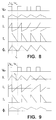
- Figures 8 and 9 show the waveforms for V gs , I 1 , I 2 , I 3 and ⁇ T over four switching cycles, respectively for when the inductance value of inductor 43 is greater than that of the transformer 42 and for when it it is less.
- the transformer With the inductance value of the inductor 43 greater than that of the transformer 42 ( Figure 8 waveforms), the transformer becomes discharged at time t X during the off period t OFF (see flux waveform ⁇ T ) and thereafter the transformer is charged by the inductor until it is equally and oppositely charged to the inductor.
- the inductor 43 With the inductance value of the inductor 43 less than that of the transformer 42 ( Figure 9 waveforms), the inductor becomes discharged at time t Y during the off period t OFF (see flux waveform ⁇ T ) and thereafter the inductor is charged by the transformer until it is equally and oppositely charged to the inductor.
- the reverse current flow through inductor 43 is permitted by a capacitor (not shown) connected across the dc side of the rectifier bridge 39; this capacitor has a high impedance at the ac mains frequency but a low impedance at the switching frequency of the switching device 44.
- the present invention can advantageously be used in conjunction with the invention described in our co-pending European Patent Application EP-A-757 428 of the same date entitled "Flyback Converter".
- a flyback converter is described in which at least part of the energy stored in the primary leakage inductance of the transformer is transferred to the converter output circuit and converted into a dc component of the converter output so that it is dissipated as useful energy in the load.
- This is achieved by providing first and second tuning capacitors connected across the transformer primary and secondary windings respectively.
- Figure 10 of the present specification shows a switched mode power supply similar in form to that of Figure 3 but provided with first and second tuning capacitances 80, 85 in accordance with the teaching of our aforesaid co-pending patent application.
- the first tuning capacitor 80 sets up a ringing on turn off of the switching device 44, this ringing being visible on the secondary side of the transformer 42.
- the second tuning capacitor 85 creates an anti-phase component to the ringing signal.
- the main ringing signal and the anti-phase component are then mixed in the non-linear device constituted by the rectifier diode 48 of the output circuit, to produce a dc component that can be dissipated in the load.
- the switching device 44 is not turned on immediately the flux in the transformer falls to zero but a short while after when the voltage across the switching device reaches a minimum as it swings down at the resonance frequency established between the capacitors 80 and 85 and the primary winding 46. The reason for doing this is to minimise the dissipation in the device 44 of energy stored in the tuning capacitor 80.
- the output of the sensing coil 60 is now connected to a 90 degree phase shifter 91 (for example, an integrator) which in turn is connected to a zero-crossing detector 92 that replaces the detector 62 of Figure 3.
- the voltage minimum occurring following the flux in transformer 42 first reaching zero is represented by a zero crossing of the signal output by the phase shifter 91 and so is detected by the zero-crossing detector 92.
Landscapes
- Engineering & Computer Science (AREA)
- Power Engineering (AREA)
- Theoretical Computer Science (AREA)
- Physics & Mathematics (AREA)
- General Engineering & Computer Science (AREA)
- General Physics & Mathematics (AREA)
- Dc-Dc Converters (AREA)
- Rectifiers (AREA)
- Supply And Distribution Of Alternating Current (AREA)
Abstract
Description
- "Reduction of voltage stress in integrated high-quality rectifier-regulators by variable frequency control" - Jovanic & Lee[APEC '94 - Ninth Annual Applied Power Electronics Conference and Exposition, vol. 2, 13-17 February 1994 Orlando, FL, USA, pages 596-575, XP 0004673666]This document describes an arrangement for reducing the voltage stress across the storage capacitor in a BIFRED or BIBRED regulator. The switching frequency is controlled as a function of the voltage across the storage capacitor.
- "Improving Power Factor Correction in Distributed Power Supply Systems using PWM and ZCS-QR SEPIC Toplogies" - Sebastion J. et al[Proceedings of the Annual Power Electronics Specialists Conference, Massachusetts, 25-27 June, 1991, no. 22, Institute of Electrical and Electronic Engineers, XP 000278420]Figure 10 of this document shows two possible control implementations of a PWM SEPIC regulator used as a power factor preregulator. In the first implementation, the "multiplier" approach is used (as described in Figure 1 of the present specification), whilst in the second implementation a "voltage follower" approach is used in which on-time duration is controlled in dependence on an output-voltage error signal.
- an energy-storing inductor,
- a switching device connected in series with said inductor across the output of the rectifier arrangement,
- a control arrangement for controlling the cyclic turning on and off of the switching device at switching frequencies substantially greater than the frequency of said ac input, and
- a coupling capacitor connected in series with the primary winding across said switching device and valued to present a low impedance at said switching frequencies but a substantially higher impedance at the frequency of said ac input;
- switch-on control means having detector means for detecting when a predetermined turn-on condition is reached in which the inductor and transformer have stored energy levels such that the inductor and transformer are equally balanced to charge one another, and turn-on means for turning on the switching device upon the detector means detecting the reaching of said predetermined turn-on condition; and
- on-time duration control means for maintaining the switching device on for a period dependent on the desired value of said regulated dc output voltage.
- a first energy-storing inductor,
- a switching device connected in series with said first inductor across the output of the rectifier arrangement,
- a control arrangement for controlling the cyclic turning on and off of the switching device at switching frequencies substantially greater than the frequency of said ac input,
- a second energy-storing inductor,
- a coupling capacitor connected in series with the second inductor across said switching device and valued to present a low impedance at said switching frequencies but a substantially higher impedance at the frequency of said ac input;
- a rectifier diode, and
- a reservoir capacitor connected in series with the diode across the second inductor, said regulated dc output voltage being developed across said reservoir capacitor;
- switch-on control means having detector means for detecting when a predetermined turn-on condition is reached in which the first and second inductors have stored energy levels such that the inductors are equally balanced to charge one another, and turn-on means for turning on the switching device upon the detector means detecting the reaching of said predetermined turn-on condition; and
- on-time duration control means for maintaining the switching device on for a period dependent on the desired value of said regulated dc output voltage.
- . Figure 1
- is a circuit diagram of a known switched mode power supply with power factor correction;
- . Figure 2
- is a circuit diagram of a SEPIC regulator forming part of the prior art;
- . Figure 3
- is a circuit diagram of a first switched mode power supply embodying the present invention;
- . Figure 4
- is a circuit diagram of the principle components of the Figure 3 switched mode power supply;
- . Figure 5
- shows voltage and current time plots illustrating operation of the Figure 4 circuit for equal inductance values of first and second inductive components of the circuit;
- . Figure 6
- is a current-time plot for the input current drawn by the Figure 4 circuit for three different values of input voltage;
- . Figure 7
- shows voltage-time plots illustrating the operation of an output-voltage feedback loop of the Figure 3 converter;
- . Figure 8
- shows voltage and current time plots similar to those of Figure 5 but illustrating operation of the Figure 4 circuit for the first inductive component of the circuit having a higher inductance value than the second inductive component;
- . Figure 9
- shows voltage and current time plots similar to those of Figure 5 but illustrating operation of the Figure 4 circuit for the first inductive component of the circuit having a lower inductance value than the second inductive component;
- . Figure 10
- is a circuit diagram of a second switched mode power supply embodying the present invention; and
- . Figure 11
- is a circuit diagram of a third switched mode power supply embodying the present invention.
- the timing of turn on of the switching device, this being synchronised to occur
immediately following the induced voltage in the transformer windings falling
to zero (this function involves
elements 60 to 65); and - the duration of the on time of the switching device, this duration being adjusted
in dependence on the value of the output voltage VO such as to keep the latter
at a predetermined level (this function involves
elements 65 to 71).
Claims (18)
- A power supply comprising a rectifier arrangement (39) for receiving an ac input and producing a rectified output at an output of the rectifier arrangement, and a flyback converter comprising an input circuit (40) connected to the output of the rectifier arrangement (39), an output circuit (41) for providing a regulated dc output voltage, and an energy-storing transformer (42) that has primary and secondary windings (46,47) respectively connected into said input and output circuits (40,41); the input circuit (40) comprising:the control arrangement comprising:an energy-storing inductor (43),a switching device (44) connected in series with said inductor (43) across the output of the rectifier arrangement (39),a control arrangement (60-71)for controlling the cyclic turning on and off of the switching device (44) at switching frequencies substantially greater than the frequency of said ac input, anda coupling capacitor (45) connected in series with the primary winding (46) across said switching device (44) and valued to present a low impedance at said switching frequencies but a substantially higher impedance at the frequency of said ac input;switch-on control means having detector means (60,62) for detecting when a predetermined turn-on condition is reached in which the inductor (43) and transformer (42) have stored energy levels such that the inductor and transformer are equally balanced to charge one another, and turn-on means (65) for turning on the switching device (44) upon the detector means detecting the reaching of said predetermined turn-on condition; andon-time duration control means (65-71) for maintaining the switching device (44) on for a period dependent on the desired value of said regulated dc output voltage.
- A power supply according to claim 1, wherein the inductance values of said inductor (43) and the transformer primary winding (46) are equal; said predetermined turn-on condition being reached when the stored energy levels in the inductor and transformer are zero.
- A power supply according to claim 1, wherein the inductance value of said inductor (43) is greater than that of the transformer primary winding (46); the transformer (42), following turn off of the switching device (44), first discharging to zero and then being recharged by the inductor (43) until said predetermined turn-on condition is reached.
- A power supply according to claim 1, wherein said detector means (60,62) of said switch-on control means comprises:said turn-on means (65) turning on the switching device (44) at a said minimum determined by said- determining means (62).sensing means (60) for deriving a voltage proportional to the rate of change of flux in the transformer (42), this rate of change falling to zero when said predetermined turn-on condition is met, anddetermining means (62) for determining a minimum of the voltage sensed by said sensing means (60);
- A power supply according to claim 4, wherein said sensing means comprises a sensing winding (60) wound jointly with said primary and secondary windings (46,47) of said transformer.
- A power supply according to claim 4, wherein said switch-on control means further comprises time-out means (64) for initiating turn on of the switching device (44) by said turn-on means a predetermined time after when switching device was last on unless the latter is earlier turned on again by said turn-on means (65).
- A power supply according to claim 1, wherein said switch-on control means comprises:said turn-on means (65) turning on the switching device when said determining means determines that the secondary winding current has fallen to zero.sensing means for monitoring the current in the transformer secondary winding (47), this current reaching zero when said predetermined turn-on condition is met, anddetermining means for determining when the secondary winding current as monitored by said sensing means falls to zero;
- A power supply according to claim 1, wherein said on-time duration control means comprises:said output-voltage feedback means including a low-pass filter (66) connected to receive an input signal representative of said output voltage and operative to produce a corresponding output signal in which the magnitude of a ripple component contained in said input signal has been substantially reduced, this ripple component corresponding to a ripple present in said output voltage at twice the frequency of the ac mains, and the output signal of the low-pass filter forming, at least in part, said feedback signal.output-voltage feedback means (66-69) for providing a feedback signal indicative of said output voltage,comparison means (71) for comparing said feedback signal with a reference in order to generate an error signal, said reference being representative of a desired value of said output voltage, andtiming means (65) for adjusting the on time of the switching device (44) such as to minimise said error signal;
- A power supply according to claim 8, wherein said output-voltage feedback means further comprises a transient accelerator (68) responsive to rapid changes and/or large changes in said output voltage to bypass the low-pass filter (66) and introduce these changes more quickly into said feedback signal.
- A power supply according to claim 8, wherein said output voltage feedback means further comprises a minimum peak detector (67) for detecting minimums in the voltage across the secondary winding (47) of the transformer on the timescale of the mains frequency, the minimum voltage detector (67) producing an output scaled and phase aligned with the output of the low-pass filter (66) such as to act to cancel any residual ripple component in the latter, the output of the minimum peak detector (67) being introduced into one of said feedback signal and said error signal.
- A power supply comprising a rectifier arrangement (39) for receiving an ac input and producing a rectified output at an output of the rectifier arrangement, and a regulator connected to the output of the rectifier arrangement and operative to provide a regulated dc output voltage; said regulator comprising:the control arrangement comprising:a first energy-storing inductor (43),a switching device (44) connected in series with said first inductor (43) across the output of the rectifier arrangement (39),a control arrangement (60-70) for controlling the cyclic turning on and off of the switching device (44) at switching frequencies substantially greater than the frequency of said ac input,a second energy-storing inductor (100),a coupling capacitor (45) connected in series with the second inductor (100) across said switching device (44) and valued to present a low impedance at said switching frequencies but a substantially higher impedance at the frequency of said ac input;a rectifier diode (48), anda reservoir capacitor (49) connected in series with the diode (48) across the second inductor (100), said regulated dc output voltage being developed across said reservoir capacitor (49);switch-on control means having detector means (62) for detecting when a predetermined turn-on condition is reached in which the first and second inductors (43,100) have stored energy levels such that the inductors are equally balanced to charge one another, and turn-on means (65) for turning on the switching device (44) upon the detector means detecting the reaching of said predetermined turn-on condition; andon-time duration control means (65-70) for maintaining the switching device (44) on for a period dependent on the desired value of said regulated dc output voltage.
- A power supply according to claim 11, wherein the inductance values of said first and second inductors (43,100) are equal; said predetermined turn-on condition being reached when the stored energy levels in the inductors are zero.
- A power supply according to claim 11, wherein the inductance value of said first inductor (43) is greater than that of the second inductor (100); the second inductor, following turn off of the switching device (44), first discharging to zero and then being recharged by the first inductor (43) until said predetermined turn-on condition is reached.
- A power supply according to claim 11, wherein the detector means of said switch-on control means comprises:said turn-on means (65) for turning on the switching device (44) at a said minimum determined by said determining means (62).sensing means for monitoring the voltage across said second inductor (43), this voltage falling to zero when said predetermined turn-on condition is met, anddetermining means (62) for determining a minimum of the voltage sensed by said sensing means;
- A power supply according to claim 14, wherein said switch-on control means further comprises time-out means (64) for initiating turn on of the switching device (44) by said turn-on means (65) a predetermined time after when switching device was last on unless the latter is earlier turned on again by said turn-on means (65).
- A power supply according to claim 11, wherein said on-time duration control means comprises:said output-voltage feedback means including a low-pass filter (66) connected to receive an input signal representative of said output voltage and operative to produce a corresponding output signal in which the magnitude of a ripple component contained in said input signal has been substantially reduced, this ripple component corresponding to a ripple present in said output voltage at twice the frequency of the ac mains, and the output signal of the low-pass filter (66) forming, at least in part, said feedback signal.output-voltage feedback means for providing a feedback signal indicative of said output voltage,comparison means (70) for comparing said feedback signal with a reference in order to generate an error signal, said reference being representative of a desired value of said output voltage, andtiming means (65) for adjusting the on time of the switching device (44) such as to minimise said error signal;
- A power supply according to claim 16, wherein said output-voltage feedback means further comprises a transient accelerator (68) responsive to rapid changes and/or large deviations in said output voltage to bypass the low-pass filter (66) and introduce these changes more quickly into said feedback signal.
- A power supply according to claim 16, wherein said output voltage feedback means further comprises a minimum peak detector (67) for detecting minimums in the voltage across the second inductor (100) on the timescale of the mains frequency, the minimum voltage detector (67) producing an output scaled and phase aligned with the output of the low-pass filter (66) such as to act to cancel any residual ripple component in the latter, the output of the minimum peak detector (67) being introduced into one of said feedback signal and said error signal.
Priority Applications (6)
| Application Number | Priority Date | Filing Date | Title |
|---|---|---|---|
| AT95410076T ATE173570T1 (en) | 1995-07-31 | 1995-07-31 | SWITCHED SWITCHING POWER SUPPLY WITH POWER FACTOR CORRECTION |
| EP95410076A EP0757429B1 (en) | 1995-07-31 | 1995-07-31 | Switched mode power supply with power factor correction |
| DE69506098T DE69506098T2 (en) | 1995-07-31 | 1995-07-31 | Switched-mode switching power supply with power factor correction |
| US08/675,301 US5682306A (en) | 1995-07-31 | 1996-07-01 | Switched mode power supply with power factor correction |
| KR1019960030804A KR100428329B1 (en) | 1995-07-31 | 1996-07-27 | Switched mode power supply with power factor correction |
| JP20154996A JP3659742B2 (en) | 1995-07-31 | 1996-07-31 | Switching mode power supply with power factor correction |
Applications Claiming Priority (1)
| Application Number | Priority Date | Filing Date | Title |
|---|---|---|---|
| EP95410076A EP0757429B1 (en) | 1995-07-31 | 1995-07-31 | Switched mode power supply with power factor correction |
Publications (2)
| Publication Number | Publication Date |
|---|---|
| EP0757429A1 EP0757429A1 (en) | 1997-02-05 |
| EP0757429B1 true EP0757429B1 (en) | 1998-11-18 |
Family
ID=8221562
Family Applications (1)
| Application Number | Title | Priority Date | Filing Date |
|---|---|---|---|
| EP95410076A Expired - Lifetime EP0757429B1 (en) | 1995-07-31 | 1995-07-31 | Switched mode power supply with power factor correction |
Country Status (6)
| Country | Link |
|---|---|
| US (1) | US5682306A (en) |
| EP (1) | EP0757429B1 (en) |
| JP (1) | JP3659742B2 (en) |
| KR (1) | KR100428329B1 (en) |
| AT (1) | ATE173570T1 (en) |
| DE (1) | DE69506098T2 (en) |
Families Citing this family (41)
| Publication number | Priority date | Publication date | Assignee | Title |
|---|---|---|---|---|
| US6072708A (en) * | 1996-08-01 | 2000-06-06 | Benchmarq Microelectronics, Inc. | Phase controlled switching regulator power supply |
| US6144565A (en) * | 1999-07-20 | 2000-11-07 | Semtech Corporation | Variation on a single-ended primary inductor converter |
| TW459438B (en) * | 1999-09-17 | 2001-10-11 | Koninkl Philips Electronics Nv | Multimode switched-mode power supply |
| WO2001020758A1 (en) * | 1999-09-17 | 2001-03-22 | Koninklijke Philips Electronics N.V. | Llc converter, and method for controlling an llc converter |
| US6487098B2 (en) | 2001-02-01 | 2002-11-26 | International Business Machines Corporation | Power factor correction (PFC) circuit that eliminates an inrush current limit circuit |
| WO2003009653A1 (en) * | 2001-07-19 | 2003-01-30 | Lumileds Lighting Us., Llc | Led switching arrangement |
| ATE326826T1 (en) * | 2001-07-19 | 2006-06-15 | Lumileds Lighting Llc | LED CIRCUIT |
| KR100418902B1 (en) * | 2001-09-06 | 2004-02-14 | 엘지전자 주식회사 | Apparatus for controlling power |
| US7123494B2 (en) * | 2003-05-06 | 2006-10-17 | Semiconductor Components Industries, L.L.C. | Power factor correction circuit and method of varying switching frequency |
| DE102004036522A1 (en) | 2004-07-28 | 2006-03-23 | Infineon Technologies Ag | Control circuit for a switch in a switching converter to improve the step response |
| DE102004038353B4 (en) * | 2004-08-06 | 2009-01-15 | Infineon Technologies Austria Ag | Control circuit for a switch in a switching converter and circuit arrangement with a switching converter and a load |
| EP1736748B1 (en) * | 2005-06-21 | 2012-05-02 | Mettler-Toledo AG | Method of processing the output signal of a mesuring transducer and force measuring device for carrying out the method. |
| KR20050088939A (en) * | 2005-07-07 | 2005-09-07 | 박은지 | Sliding door closer |
| DE102006047065B4 (en) | 2006-10-05 | 2018-07-26 | Stephan Hoffmann | Circuit and method for voltage division |
| US7944153B2 (en) * | 2006-12-15 | 2011-05-17 | Intersil Americas Inc. | Constant current light emitting diode (LED) driver circuit and method |
| US8060218B2 (en) | 2007-08-02 | 2011-11-15 | Synecor, Llc | Inductive element for intravascular implantable devices |
| US8508166B2 (en) | 2009-08-10 | 2013-08-13 | Emerson Climate Technologies, Inc. | Power factor correction with variable bus voltage |
| US8698433B2 (en) | 2009-08-10 | 2014-04-15 | Emerson Climate Technologies, Inc. | Controller and method for minimizing phase advance current |
| US8358098B2 (en) * | 2009-08-10 | 2013-01-22 | Emerson Climate Technologies, Inc. | System and method for power factor correction |
| US8493014B2 (en) * | 2009-08-10 | 2013-07-23 | Emerson Climate Technologies, Inc. | Controller and method for estimating, managing, and diagnosing motor parameters |
| US8406021B2 (en) * | 2009-08-10 | 2013-03-26 | Emerson Climate Technologies, Inc. | System and method for reducing line current distortion |
| US8476873B2 (en) * | 2009-08-10 | 2013-07-02 | Emerson Climate Technologies, Inc. | System and method for current balancing |
| US8264192B2 (en) | 2009-08-10 | 2012-09-11 | Emerson Climate Technologies, Inc. | Controller and method for transitioning between control angles |
| US8344706B2 (en) * | 2009-08-10 | 2013-01-01 | Emerson Climate Technologies, Inc. | System and method for rejecting DC current in power factor correction systems |
| US8264860B2 (en) * | 2009-08-10 | 2012-09-11 | Emerson Climate Technologies, Inc. | System and method for power factor correction frequency tracking and reference generation |
| SG188475A1 (en) * | 2010-09-08 | 2013-04-30 | Huizhou Light Engine Ltd | Stabilization circuit for electronic transformer driven led devices |
| US8754705B2 (en) * | 2011-08-01 | 2014-06-17 | Crestron Electronics Inc. | Audio amplifier power supply with inherent power factor correction |
| JP5773435B2 (en) * | 2011-10-25 | 2015-09-02 | ニチコン株式会社 | Charger |
| US9634593B2 (en) | 2012-04-26 | 2017-04-25 | Emerson Climate Technologies, Inc. | System and method for permanent magnet motor control |
| US9240749B2 (en) | 2012-08-10 | 2016-01-19 | Emerson Climate Technologies, Inc. | Motor drive control using pulse-width modulation pulse skipping |
| JP5701283B2 (en) * | 2012-12-25 | 2015-04-15 | オムロンオートモーティブエレクトロニクス株式会社 | Charger |
| KR20140105658A (en) * | 2013-02-22 | 2014-09-02 | 주식회사 하이딥 | Led lighting device using ballast |
| US9214855B2 (en) | 2013-05-03 | 2015-12-15 | Cooper Technologies Company | Active power factor correction circuit for a constant current power converter |
| US9548794B2 (en) | 2013-05-03 | 2017-01-17 | Cooper Technologies Company | Power factor correction for constant current input with power line communication |
| US9190901B2 (en) | 2013-05-03 | 2015-11-17 | Cooper Technologies Company | Bridgeless boost power factor correction circuit for constant current input |
| US9000736B2 (en) | 2013-05-03 | 2015-04-07 | Cooper Technologies Company | Power factor correction algorithm for arbitrary input waveform |
| US10890932B2 (en) | 2018-08-20 | 2021-01-12 | Eaton Intelligent Power Limited | Electrical network configured to magnetically couple to a winding and to control magnetic saturation in a magnetic core |
| JP7327110B2 (en) * | 2019-11-26 | 2023-08-16 | サンケン電気株式会社 | DC-DC converter |
| US11735923B2 (en) | 2020-07-28 | 2023-08-22 | Eaton Intelligent Power Limited | Voltage regulation device that includes a converter for harmonic current compensation and reactive power management |
| JP7528779B2 (en) | 2020-12-24 | 2024-08-06 | 富士電機株式会社 | Switching control circuits, power supply circuits |
| CN114156872B (en) * | 2021-11-24 | 2024-07-19 | 万龙时代科技有限公司 | Intelligent current distribution method |
Family Cites Families (6)
| Publication number | Priority date | Publication date | Assignee | Title |
|---|---|---|---|---|
| US4184197A (en) * | 1977-09-28 | 1980-01-15 | California Institute Of Technology | DC-to-DC switching converter |
| US4257087A (en) * | 1979-04-02 | 1981-03-17 | California Institute Of Technology | DC-to-DC switching converter with zero input and output current ripple and integrated magnetics circuits |
| US4739462A (en) * | 1984-12-26 | 1988-04-19 | Hughes Aircraft Company | Power supply with noise immune current sensing |
| US5134355A (en) * | 1990-12-31 | 1992-07-28 | Texas Instruments Incorporated | Power factor correction control for switch-mode power converters |
| US5442539A (en) * | 1992-10-02 | 1995-08-15 | California Institute Of Technology | CuK DC-to-DC switching converter with input current shaping for unity power factor operation |
| US5442534A (en) * | 1993-02-23 | 1995-08-15 | California Institute Of Technology | Isolated multiple output Cuk converter with primary input voltage regulation feedback loop decoupled from secondary load regulation loops |
-
1995
- 1995-07-31 EP EP95410076A patent/EP0757429B1/en not_active Expired - Lifetime
- 1995-07-31 AT AT95410076T patent/ATE173570T1/en not_active IP Right Cessation
- 1995-07-31 DE DE69506098T patent/DE69506098T2/en not_active Expired - Fee Related
-
1996
- 1996-07-01 US US08/675,301 patent/US5682306A/en not_active Expired - Lifetime
- 1996-07-27 KR KR1019960030804A patent/KR100428329B1/en not_active IP Right Cessation
- 1996-07-31 JP JP20154996A patent/JP3659742B2/en not_active Expired - Fee Related
Also Published As
| Publication number | Publication date |
|---|---|
| JPH09121539A (en) | 1997-05-06 |
| DE69506098T2 (en) | 1999-04-15 |
| US5682306A (en) | 1997-10-28 |
| JP3659742B2 (en) | 2005-06-15 |
| KR970007578A (en) | 1997-02-21 |
| EP0757429A1 (en) | 1997-02-05 |
| DE69506098D1 (en) | 1998-12-24 |
| KR100428329B1 (en) | 2004-07-12 |
| ATE173570T1 (en) | 1998-12-15 |
Similar Documents
| Publication | Publication Date | Title |
|---|---|---|
| EP0757429B1 (en) | Switched mode power supply with power factor correction | |
| US7180273B2 (en) | Low switching frequency power factor correction circuit | |
| JP3230052B2 (en) | Power supply | |
| US5642267A (en) | Single-stage, unity power factor switching converter with voltage bidirectional switch and fast output regulation | |
| US5001620A (en) | Power factor improvement | |
| US5008794A (en) | Regulated flyback converter with spike suppressing coupled inductors | |
| US6005781A (en) | Two switch off-line switching converter | |
| US20070035971A1 (en) | Switching power supply circuit | |
| JP2017017767A (en) | High efficiency power factor improvement circuit and switching power supply device | |
| KR100544186B1 (en) | Apparatus for providing power | |
| JPH05276750A (en) | Power supply circuit | |
| JP3588429B2 (en) | Power converter | |
| JP2653712B2 (en) | Switching regulator | |
| JP2512040B2 (en) | Power supply | |
| Comandatore et al. | Designing a high power factor switching preregulator with the L4981 continuous mode | |
| JPS58107267A (en) | Electric power source for welding | |
| JP2002034255A (en) | Power supply apparatus | |
| JPS61288730A (en) | Power source unit | |
| JPH09131056A (en) | Power-factor improved converter circuit | |
| JPH01152956A (en) | Power unit | |
| JPH04178170A (en) | Power factor improving type rectifying apparatus | |
| CN115706531A (en) | Power converter controller, power converter and method for operating power converter | |
| JP4228266B2 (en) | DC variable voltage power supply | |
| JP3028026B2 (en) | Switching power supply | |
| JPH0421360A (en) | Switching regulator |
Legal Events
| Date | Code | Title | Description |
|---|---|---|---|
| PUAI | Public reference made under article 153(3) epc to a published international application that has entered the european phase |
Free format text: ORIGINAL CODE: 0009012 |
|
| AK | Designated contracting states |
Kind code of ref document: A1 Designated state(s): AT DE FR GB IT NL SE |
|
| 17P | Request for examination filed |
Effective date: 19970714 |
|
| 17Q | First examination report despatched |
Effective date: 19971030 |
|
| GRAG | Despatch of communication of intention to grant |
Free format text: ORIGINAL CODE: EPIDOS AGRA |
|
| GRAG | Despatch of communication of intention to grant |
Free format text: ORIGINAL CODE: EPIDOS AGRA |
|
| GRAH | Despatch of communication of intention to grant a patent |
Free format text: ORIGINAL CODE: EPIDOS IGRA |
|
| GRAH | Despatch of communication of intention to grant a patent |
Free format text: ORIGINAL CODE: EPIDOS IGRA |
|
| GRAH | Despatch of communication of intention to grant a patent |
Free format text: ORIGINAL CODE: EPIDOS IGRA |
|
| GRAA | (expected) grant |
Free format text: ORIGINAL CODE: 0009210 |
|
| AK | Designated contracting states |
Kind code of ref document: B1 Designated state(s): AT DE FR GB IT NL SE |
|
| PG25 | Lapsed in a contracting state [announced via postgrant information from national office to epo] |
Ref country code: SE Free format text: THE PATENT HAS BEEN ANNULLED BY A DECISION OF A NATIONAL AUTHORITY Effective date: 19981118 Ref country code: AT Free format text: LAPSE BECAUSE OF FAILURE TO SUBMIT A TRANSLATION OF THE DESCRIPTION OR TO PAY THE FEE WITHIN THE PRESCRIBED TIME-LIMIT Effective date: 19981118 |
|
| REF | Corresponds to: |
Ref document number: 173570 Country of ref document: AT Date of ref document: 19981215 Kind code of ref document: T |
|
| REF | Corresponds to: |
Ref document number: 69506098 Country of ref document: DE Date of ref document: 19981224 |
|
| ET | Fr: translation filed | ||
| ITF | It: translation for a ep patent filed | ||
| PLBE | No opposition filed within time limit |
Free format text: ORIGINAL CODE: 0009261 |
|
| STAA | Information on the status of an ep patent application or granted ep patent |
Free format text: STATUS: NO OPPOSITION FILED WITHIN TIME LIMIT |
|
| 26N | No opposition filed | ||
| REG | Reference to a national code |
Ref country code: GB Ref legal event code: 732E |
|
| NLS | Nl: assignments of ep-patents |
Owner name: HEWLETT-PACKARD COMPANY (A DELAWARE CORPORATION) |
|
| REG | Reference to a national code |
Ref country code: GB Ref legal event code: IF02 |
|
| REG | Reference to a national code |
Ref country code: FR Ref legal event code: TP |
|
| PGFP | Annual fee paid to national office [announced via postgrant information from national office to epo] |
Ref country code: DE Payment date: 20070831 Year of fee payment: 13 |
|
| PGFP | Annual fee paid to national office [announced via postgrant information from national office to epo] |
Ref country code: GB Payment date: 20070727 Year of fee payment: 13 |
|
| PGFP | Annual fee paid to national office [announced via postgrant information from national office to epo] |
Ref country code: NL Payment date: 20070724 Year of fee payment: 13 Ref country code: IT Payment date: 20070727 Year of fee payment: 13 |
|
| PGFP | Annual fee paid to national office [announced via postgrant information from national office to epo] |
Ref country code: FR Payment date: 20070717 Year of fee payment: 13 |
|
| GBPC | Gb: european patent ceased through non-payment of renewal fee |
Effective date: 20080731 |
|
| NLV4 | Nl: lapsed or anulled due to non-payment of the annual fee |
Effective date: 20090201 |
|
| PG25 | Lapsed in a contracting state [announced via postgrant information from national office to epo] |
Ref country code: DE Free format text: LAPSE BECAUSE OF NON-PAYMENT OF DUE FEES Effective date: 20090203 |
|
| REG | Reference to a national code |
Ref country code: FR Ref legal event code: ST Effective date: 20090331 |
|
| PG25 | Lapsed in a contracting state [announced via postgrant information from national office to epo] |
Ref country code: NL Free format text: LAPSE BECAUSE OF NON-PAYMENT OF DUE FEES Effective date: 20090201 |
|
| PG25 | Lapsed in a contracting state [announced via postgrant information from national office to epo] |
Ref country code: GB Free format text: LAPSE BECAUSE OF NON-PAYMENT OF DUE FEES Effective date: 20080731 |
|
| PG25 | Lapsed in a contracting state [announced via postgrant information from national office to epo] |
Ref country code: IT Free format text: LAPSE BECAUSE OF NON-PAYMENT OF DUE FEES Effective date: 20080731 Ref country code: FR Free format text: LAPSE BECAUSE OF NON-PAYMENT OF DUE FEES Effective date: 20080731 |