EP0751398B1 - Coordinate input device using Mateucci effect - Google Patents
Coordinate input device using Mateucci effect Download PDFInfo
- Publication number
- EP0751398B1 EP0751398B1 EP96113405A EP96113405A EP0751398B1 EP 0751398 B1 EP0751398 B1 EP 0751398B1 EP 96113405 A EP96113405 A EP 96113405A EP 96113405 A EP96113405 A EP 96113405A EP 0751398 B1 EP0751398 B1 EP 0751398B1
- Authority
- EP
- European Patent Office
- Prior art keywords
- magnetic
- coordinate
- wire
- wires
- voltage
- Prior art date
- Legal status (The legal status is an assumption and is not a legal conclusion. Google has not performed a legal analysis and makes no representation as to the accuracy of the status listed.)
- Expired - Lifetime
Links
Images

Classifications
-
- G—PHYSICS
- G01—MEASURING; TESTING
- G01R—MEASURING ELECTRIC VARIABLES; MEASURING MAGNETIC VARIABLES
- G01R33/00—Arrangements or instruments for measuring magnetic variables
- G01R33/20—Arrangements or instruments for measuring magnetic variables involving magnetic resonance
- G01R33/24—Arrangements or instruments for measuring magnetic variables involving magnetic resonance for measuring direction or magnitude of magnetic fields or magnetic flux
-
- G—PHYSICS
- G06—COMPUTING; CALCULATING OR COUNTING
- G06F—ELECTRIC DIGITAL DATA PROCESSING
- G06F3/00—Input arrangements for transferring data to be processed into a form capable of being handled by the computer; Output arrangements for transferring data from processing unit to output unit, e.g. interface arrangements
- G06F3/01—Input arrangements or combined input and output arrangements for interaction between user and computer
- G06F3/03—Arrangements for converting the position or the displacement of a member into a coded form
- G06F3/041—Digitisers, e.g. for touch screens or touch pads, characterised by the transducing means
- G06F3/046—Digitisers, e.g. for touch screens or touch pads, characterised by the transducing means by electromagnetic means
-
- G—PHYSICS
- G01—MEASURING; TESTING
- G01B—MEASURING LENGTH, THICKNESS OR SIMILAR LINEAR DIMENSIONS; MEASURING ANGLES; MEASURING AREAS; MEASURING IRREGULARITIES OF SURFACES OR CONTOURS
- G01B7/00—Measuring arrangements characterised by the use of electric or magnetic techniques
- G01B7/004—Measuring arrangements characterised by the use of electric or magnetic techniques for measuring coordinates of points
-
- G—PHYSICS
- G01—MEASURING; TESTING
- G01D—MEASURING NOT SPECIALLY ADAPTED FOR A SPECIFIC VARIABLE; ARRANGEMENTS FOR MEASURING TWO OR MORE VARIABLES NOT COVERED IN A SINGLE OTHER SUBCLASS; TARIFF METERING APPARATUS; MEASURING OR TESTING NOT OTHERWISE PROVIDED FOR
- G01D5/00—Mechanical means for transferring the output of a sensing member; Means for converting the output of a sensing member to another variable where the form or nature of the sensing member does not constrain the means for converting; Transducers not specially adapted for a specific variable
- G01D5/12—Mechanical means for transferring the output of a sensing member; Means for converting the output of a sensing member to another variable where the form or nature of the sensing member does not constrain the means for converting; Transducers not specially adapted for a specific variable using electric or magnetic means
- G01D5/14—Mechanical means for transferring the output of a sensing member; Means for converting the output of a sensing member to another variable where the form or nature of the sensing member does not constrain the means for converting; Transducers not specially adapted for a specific variable using electric or magnetic means influencing the magnitude of a current or voltage
-
- G—PHYSICS
- G01—MEASURING; TESTING
- G01D—MEASURING NOT SPECIALLY ADAPTED FOR A SPECIFIC VARIABLE; ARRANGEMENTS FOR MEASURING TWO OR MORE VARIABLES NOT COVERED IN A SINGLE OTHER SUBCLASS; TARIFF METERING APPARATUS; MEASURING OR TESTING NOT OTHERWISE PROVIDED FOR
- G01D5/00—Mechanical means for transferring the output of a sensing member; Means for converting the output of a sensing member to another variable where the form or nature of the sensing member does not constrain the means for converting; Transducers not specially adapted for a specific variable
- G01D5/48—Mechanical means for transferring the output of a sensing member; Means for converting the output of a sensing member to another variable where the form or nature of the sensing member does not constrain the means for converting; Transducers not specially adapted for a specific variable using wave or particle radiation means
- G01D5/485—Mechanical means for transferring the output of a sensing member; Means for converting the output of a sensing member to another variable where the form or nature of the sensing member does not constrain the means for converting; Transducers not specially adapted for a specific variable using wave or particle radiation means using magnetostrictive devices
-
- G—PHYSICS
- G01—MEASURING; TESTING
- G01R—MEASURING ELECTRIC VARIABLES; MEASURING MAGNETIC VARIABLES
- G01R33/00—Arrangements or instruments for measuring magnetic variables
- G01R33/02—Measuring direction or magnitude of magnetic fields or magnetic flux
-
- G—PHYSICS
- G01—MEASURING; TESTING
- G01R—MEASURING ELECTRIC VARIABLES; MEASURING MAGNETIC VARIABLES
- G01R33/00—Arrangements or instruments for measuring magnetic variables
- G01R33/02—Measuring direction or magnitude of magnetic fields or magnetic flux
- G01R33/10—Plotting field distribution ; Measuring field distribution
Definitions
- the present invention relates to a coordinate input device using Matteucci effect.
- a prior art magnetic image sensor for detecting magnetic data on a multi-track of a magnetic card or the like or a magnetic field caused by a magnetic material film uses a gap type magnetic head of multi-channel, a magnetic resistive element array, a Hall-effect element array, or the like.
- the prior art magnetic image sensor has been defective in that the magnetic image sensor is expensive and requires the number of detection circuits corresponding to the multi-channel and thus its necessary circuit is increased in size.
- EP-A-0 187 372 disclosed a position detecting device. It includes a tablet with a magnetic sheet and two conductor sheets.
- the magnetic sheet is formed by weaving a group of warp elements composed of a multiplicity of insulating fibres and a plurality of relatively long magnetic elements disposed among the insulating fibres at predetermined regular spacings and a group of weft elements composed of a multiplicity of insulating fibres into a plain weave fabric, and hardening this fabric into a sheet like configuration by means of an insulating resin.
- a plurality of magnetic wires circumferentially magnetized therein are arranged to form a wire array and, when a coordinate designator for generating an A.C. magnetic field is moved close to the wire array, a coordinate position of the designator on the wire array is calculated and found on the basis of a mutual relationship between pulse voltages developed across the respective magnetic wires.
- a plurality of exciting coils for generating a predetermind A.C. magnetic field may further be arranged along a magnetic wire circumferentially magnetized therein and a static magnetic field to be image-detected is positioned along the wire, so that its magnetic image is detected on the basis of the magnitude of a pulse voltage developed across the wire when the exciting coils are sequentially excited one after another.
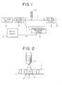
- a signal detecting section of a coordinate input device in accordance with the present invention, wherein a magnetic wire 1 is used as a coordinate detector and an A.C. magnetic field is applied to a coordinate designator through the magnetic wire 1 and an electromagnet 2 for coordinate designation (or coordinate designator 2).
- a D.C. bias circuit 4 is provided to pass a D.C. current through the magnetic wire 1 to provide a circumferential magnetization therein.
- the D.C. bias circuit 4 is connected to the magnetic wire 1 through a wiring line, this causes the impedance of the magnetic wire 1 at its both ends to be reduced, thus reducing a pulse voltage to be developed in the magnetic wire 1.
- the high impedance circuit 3 is provided to at least one end of the magnetic wire 1.
- the pulse voltage thus developed in the magnetic wire 1 appears at both ends P and Q of the magnetic wire 1.
- the pulse voltage is detected by a double-frequency detecting circuit 5 with respect to its 2f component.
- the double-frequency detecting circuit 5 may comprise an ordinary resonance circuit, filter circuit or synchronous detector circuit.
- a control circuit 6 functions to supply an exciting current having a fundamental frequency 1f to the electromagnet 2 for coordination designation and also to supply a control signal having a fundamental frequency 2f to the double-frequency detecting circuit 5 as necessary.
- Fig. 2 shows a pulse-voltage generating principle for explaining how to generate the pulse voltage when the circumferentially-magnetized magnetic wire 1 is subjected to an A.C. magnetic field.
- the circumferential magnetization of the magnetic wire 1 is repetitively subjected to partial inverting and restoring movements under the influence of the alternating magnetic field of the coordiante designating electromagnet 2.
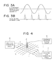
- the magnetic field of the electromagnet and the then pulse voltage developed across the magnetic wire are shown in Figs. 3A and 3B. More specifically, the number of inversions in the magnetization varies depending on the composite value of the magnetic field generated by the electromagnet and the magnetic field based on terrestrial magnetism.
- the frequency components of the voltage developed across the magnetic wire include composite values of the respective frequency components of 1f, 2f, 3f, ... where f denotes a frequency at which the electromagnet is excited.
- the 1f component varies largely with the alternating magnetic field, but the 2f component less varies, since the 2f component is derived from pulses having the same wave-form as will be appreciated from Fig. 3B. For this reason, it is effective to detect the 2f component by the pulse voltage occurring in the magnetic wire and therefore the double-frequency detecting circuit 5 in Fig. 1 is arranged to detect the 2f component.
- the D.C. bias circuit 4 is used.
- the circuit 4 can control of the quantity of the aforementioned D.C. current. Further, by increasing the current supplied to the magnetic wire, the influence of the external magnetic field such as terrestrial magnetism can be made less.
- Fig. 4 Conceptionally shown in Fig. 4 is a coordinate input device wherein the detection section of Fig. 1 is arranged in the form of an X-Y matrix. More in detail, in order to detect a position of the coordinate designating electromagnet 2, a plurality of the magnetic wires 1 are provided in X and Y directions. Though only a Y-direction voltage detector for the magnetic wire 1 has been illustrated in Fig. 4, an X-direction voltage detector having the same function as the Y-direction voltage detector is also provided in actual applications. A detection-side terminating circuit 7, which has the same function as the A.C. high impedance circuit 3 in Fig.
- a drive-side terminating circuit 8 includes such a D.C. current bias circuit 4 and an A.C. high impedance circuit 3 connected to the circuit 4 as necessary as shown in Fig. 4.
- a coordinate detection control circuit 9 acts to excite the electromagnet 2 for coordinate designation and also to generate a timing signal for controlling the function of the double-frequency detecting circuit and the function of the multiplexing circuit. The structures of these circuits will be detailed later.
- the coordinate input device detects voltages developed (when the circumferential magnetization of the magnetic wires is inverted) in ones of the circumferentially-magnetized magnetic wires when the coordinate designator excited with an A.C. current approaches thereto.
- Such a coordiante input device is effective because it is based on a new detection principle that the magnetic wires as coordinate detectors require no windings or the like for voltage generation.
- a voltage is developed between both ends of the magnetic wire, when a multiplicity of magnetic wires for coordinate detection are arranged in the form of an array, the both ends of each magnetic wire is spaced by a relatively long distance. For this reason, a signal return path for connecting the both ends of the magnetic wire is necessary.
- electromagnetic magnetic coupling between the external field and a loop coil comprising the magnetic wire and the return path causes generation of a coupling signal, in addition to the original coordiante detection signal caused by the inversion in the magnetization of the magnetic wire.
- the coupling signal becomes larger than the voltage component caused by the invention in the circumferential magnetization of the magnetic wire, which results in reduction of S/N ratio of the coordiante detection signal.
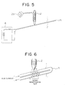
- the magnetization reversal signal is added to the voltages generated by the magnetic wires of the go and return paths on the detection principle of the circumferentially magnetized magnetic wire, whereby the detection voltage can be obtained which corresponds to twice the detection voltage obtained when the go path is made in the form of a magnetic wire and the return path is made in the form of an ordinary conductor. This case will be detailed in connection with an embodiment shown in Figs. 5 and 6.
- the magnetic wire 1 as a go path is connected at a fixed turn point 1R to a magnetic wire 1' as a return path.
- the D.C. bias circuit 4 is used to provide circumferential magnetization to the both wires.
- the coordinate designator 2 excited by an A.C. signal source 2S applies an A.C. magnetic field to the both magnetic wires.
- the operational principle of the coordinate detector is shown in Fig. 6, wherein a bias current shown by arrows causes such circumferential magnetization as shown in Fig. 6 to be developed in the interiors of the magnetic wires 1 and 1' of the go and return paths.
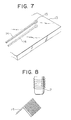
- FIG. 7 Shown in Fig. 7 is another embodiment in which magnetic materials 14 each in the form of a thin magnetic wire pattern is bonded or deposited as fixed onto the front and back surfaces of a substrate 13.
- a through hole 15 made in the substrate 13 is for interconnection between the patterns provided on the front and back sides of the substrate.
- this can be realized by depositing a magnetic film on each of the entire front and back sides of the substrate and then etching the substrate to leave the thin magnetic patterns 14 thereon.
- this can be realized by constructing the substrate in the form of a multiple layer.
- Fig. 8 shows another embodiment wherein the magnetic material 41 is made in the form of a thin magnetic pattern of repetitive magnetic lines to add together detection voltages developed in the magnetic lines to obtain a high total detection voltage and thus a high sensitivity.
- a proximity sensor which detects a vertical distance with respect to the coordinate designator 2 with a high sensitivity. It goes without saying that such a thin magnetic pattern 14 of repetitive magnetic lines as shown in Fig. 8 may be replaced by a single wire as necessary to form the proximity sensor.
- the magnetic wire or magnetic material mentioned above may be made of preferably material having a negative magnetostrictive coefficient such as amorphous material.
- reference numeral 18 denotes a matrix of repetitively turned magnetic wires arranged as equi-spaced in X and Y directions. One ends of all the magnetic wires are connected through a line 19 to the D.C. bias circuit 4 which supplies a constant current; while the other ends of all the magnetic wires are connected to collectors of switching transistors of X- and Y-decoders 20 and 21. The switching transistors are also connected at their emitters to a common circuit part.
- a wire selection circuit 23 supplies a switching signal to the bases of the switching transistors of the X- and Y- decoders 20 and 21 to sequentially turn ON the transistors one after another and to sequentially switch ON the wires one after another to sequentially supply a bias current thereto.
- a coordinate detection control circuit 9 supplies a timing pulse for wire selection to the wire selection circuit 23 and also supplies an A.C. current to the coordinate designator 2 to generate an A.C. magnetic field therein.
- a pulse voltage as shown in Fig. 3B appears on the line 19.
- the pulse voltage is sent through a resistor/capacitor coupling circuit 25 to a detection circuit 26 to be detected thereat.
- the pulse voltage is sample-held at a sample/hold circuit 27, converted into a digital signal at an A/D covnerter 28, subjected to a signal processing at a CPU 29, and then transmitted to a host computer (not shown) as a coordinate data.
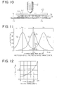
- the wire matrix is constructed so that, as shown in Fig. 10, magnetic wires 1X and 1X' for detection of X-direction coordinate magnetic wires 1Y and 1Y' for detection of Y-direction coordinate are arranged at regular intervals on a panel 30 which acts to stabilize a vertical distance between the coordinate designator 2 and the magnetic wires and also to fixedly mount the magnetic wires thereto.
- the wires 1X, 1X' and 1Y, 1Y' are arranged as bent or turned as shown in Figs. 5 and 6 respectively, and an insulator 31 is disposed between the associated wires to avoid any short-circuiting of the generation voltage caused by the rotary magnetization. Further, another insulator 31 is disposed between the X- and Y-direction wires.
- a multiplicity of magnetic wires are arranged in the X and Y directions to generate detection outputs indicative of a distance between the coordinate designator and ones of the wires close to the designator, so that the detection outputs of the associated magnetic wires made high when subjected to the A.C. magnetic field of the coordinate designator are used to carry out a coordinate estimation computation.
- the coordinate input device can have a resolution of 0.1 mm. This computation is carried out in the CPU 29 in Fig. 9.
- Fig. 11 shows Matteucci effect voltage characteristics V N-1 , V N , and V N+1 detected across three wires N-1, N, and N+1 when the coordinate designator is positioned at points spaced by a distance S from the centers of these wires, respectively.
- the distance between the wires is set to be 5 mm.
- the shape of the characteristic of Fig. 12 is identical or symmetrical with respect to each wire position in the left and right directions.
- the position ⁇ of the coordinate designator from the wire N producing the largest detection voltage can be calculated on the basis of the ratio (V N+1 /V N ) between the detection voltages of the wire N and adjacent wire N+1 respectively having the largest and the next largest values in the detection voltages of the wires, and then a coordinate point indicate of the coordinate designator can be calculated on the basis of the position ⁇ .
- a detection signal is input from a wire in a step 40 and it is judged in a step 41 whether or not the input signal is larger than a predetermined value. Determination of NO in the step 41 causes control to proceed to a step 43. Determination of YES in the step 41 causes control to go to a step 42 where the coordinate valus of the wire and the size of the detection signal are recorded in the memory and control goes to the step 43. In the step 43, it is judged whether or not detection of all the wires has been completed. Determination of NO in the step 43 causes control to go back to the step 40 to input the detection signal of the next wire.
- Determination of YES causes control to proceed to a step 44 to find detection signals V N-1 , V N , V N+1 , ... which have been judged as having predetermined continuous values.
- a next step 45 one of these detection signals having a maximum value, for example, the signal V N is determined.
- a next step 46 comparison is made in a next step 46 between the detection signals V N-1 and V N+1 of the wires N-1 and N+1 adjacent to the wire N which produced the maximum detection signal.
- control goes to a step 47 to calculate a value V N-1 /V N .
- a value ⁇ is found by referencing a table (stored in the memory) having the characteristic as shown in Fig. 12.
- the value ⁇ is subtracted from the coordinate value of the wire N and then a coordinate point at which the coordinate designator is positioned is calculated.
- the value ⁇ is found by referencing the table according to the calculated value V N+1 /V N .
- the value ⁇ is added to the coordinate value of the wire N to find a coordinate point indicative of the position of the coordinate designator.
- the coordinate calculation is completed.
- Provision of the circumferential magnetization to a magnetic wire having a magnetostrictive coefficient of zero to a negative value can be realized by providing a suitable twist to the magnetic wire to give it a twisting stress.
- the external magnetic field acts as a modulation signal when the exciting magnetic field is considered to be a carrier, and thus separate detection of the external magnetic field can be realized by processing the signal caused by the magnetization inversion. Detection of the external magnetic field can be attained with a high resolution by narrowing the range of the exciting magnetic field and this can be realized with use of a ferrite core wound by a winding.
Description
- The present invention relates to a coordinate input device using Matteucci effect.
- When circumferential magnetization is provided to the interior of a single magnetic wire and external A.C. magnetic field is applied to the wire in the transverse direction thereof, a pulsative voltage is developed across the wire, that is, a so-called Mattecci effect takes place. Such Matteucci effect is known but its substantially no application techniques are known.
- Further, as a digitizer or a coordinate input device for inputting handwritten letters, such a prior art device as shown in JP-A-61-70628 is known, but such a coordinate input device based on the aforementioned Matteucci effect is not known so far.
- Meanwhile, a prior art magnetic image sensor for detecting magnetic data on a multi-track of a magnetic card or the like or a magnetic field caused by a magnetic material film uses a gap type magnetic head of multi-channel, a magnetic resistive element array, a Hall-effect element array, or the like. Thus, the prior art magnetic image sensor has been defective in that the magnetic image sensor is expensive and requires the number of detection circuits corresponding to the multi-channel and thus its necessary circuit is increased in size.
- EP-A-0 187 372 disclosed a position detecting device. It includes a tablet with a magnetic sheet and two conductor sheets. The magnetic sheet is formed by weaving a group of warp elements composed of a multiplicity of insulating fibres and a plurality of relatively long magnetic elements disposed among the insulating fibres at predetermined regular spacings and a group of weft elements composed of a multiplicity of insulating fibres into a plain weave fabric, and hardening this fabric into a sheet like configuration by means of an insulating resin.
- It is therefore object of the present invention to provide a coordinate input device based on Matteurcci effect.
- In accordance with a coordinate input device of the present invention, a plurality of magnetic wires circumferentially magnetized therein are arranged to form a wire array and, when a coordinate designator for generating an A.C. magnetic field is moved close to the wire array, a coordinate position of the designator on the wire array is calculated and found on the basis of a mutual relationship between pulse voltages developed across the respective magnetic wires.
- A plurality of exciting coils for generating a predetermind A.C. magnetic field may further be arranged along a magnetic wire circumferentially magnetized therein and a static magnetic field to be image-detected is positioned along the wire, so that its magnetic image is detected on the basis of the magnitude of a pulse voltage developed across the wire when the exciting coils are sequentially excited one after another.
- Fig. 1 is a schematic block diagram of a signal detector which forms a major part of a coordinate input device in accordance with the present invention:
- Fig. 2 conceptionally shows a principle on how a pulse voltage is developed across a magnetic wire circumferentially magnetized therein;
- Figs. 3A and 3B are waveforms of an A.C. magnetic field and a pulse voltage generated on the above principle respectively;
- Fig. 4 shows a concept of a coordinate input device in accordance with the present invention;
- Fig. 5 shows a conceptional basic arrangement of another embodiment of the present invention for explaining its coordinate detecting operation;
- Fig. 6 is a diagram for explaining how the circumferential magnetization of a magnetic wire is rotated by an external magnetic field;
- Fig. 7 is a diagram showing how magnetic materials are fixed onto a substrate;
- Fig. 8 shows the concept of a high-sensitivity sensor for measuring a vertical distance between an electromagnet and a magnetic wire pattern;
- Fig. 9 is a block diagram of a general arrangement of a coordinate input device of the present invention;
- Fig. 10 is a cross-sectional view of a coordinate detector showing the structure of an array of magnetic wires arranged in X and Y directions;
- Fig. 11 is a characteristic diagram showing relationships between Matteucci-effect voltages developed across adjacent wires and distances from the centers of the respective wires;
- Fig. 12 is a characteristic diagram showing a relationship between the distance and a ratio between voltages detected across the adjacent wires;
- Fig. 13 is a flowchart showing the coordinate calculation procedure of the coordinate input device;
-
- Referring to Fig. 1, there is shown a signal detecting section of a coordinate input device in accordance with the present invention, wherein a
magnetic wire 1 is used as a coordinate detector and an A.C. magnetic field is applied to a coordinate designator through themagnetic wire 1 and anelectromagnet 2 for coordinate designation (or coordinate designator 2). AD.C. bias circuit 4 is provided to pass a D.C. current through themagnetic wire 1 to provide a circumferential magnetization therein. When theD.C. bias circuit 4 is connected to themagnetic wire 1 through a wiring line, this causes the impedance of themagnetic wire 1 at its both ends to be reduced, thus reducing a pulse voltage to be developed in themagnetic wire 1. For the purpose of avoiding such impedance reduction, an A.C.high impedance circuit 3 is provided to at least one end of themagnetic wire 1. The pulse voltage thus developed in themagnetic wire 1 appears at both ends P and Q of themagnetic wire 1. The pulse voltage is detected by a double-frequency detecting circuit 5 with respect to its 2f component. The double-frequency detecting circuit 5 may comprise an ordinary resonance circuit, filter circuit or synchronous detector circuit. A control circuit 6 functions to supply an exciting current having a fundamental frequency 1f to theelectromagnet 2 for coordination designation and also to supply a control signal having afundamental frequency 2f to the double-frequency detecting circuit 5 as necessary. - Fig. 2 shows a pulse-voltage generating principle for explaining how to generate the pulse voltage when the circumferentially-magnetized
magnetic wire 1 is subjected to an A.C. magnetic field. The circumferential magnetization of themagnetic wire 1 is repetitively subjected to partial inverting and restoring movements under the influence of the alternating magnetic field of the coordiante designatingelectromagnet 2. The magnetic field of the electromagnet and the then pulse voltage developed across the magnetic wire are shown in Figs. 3A and 3B. More specifically, the number of inversions in the magnetization varies depending on the composite value of the magnetic field generated by the electromagnet and the magnetic field based on terrestrial magnetism. The frequency components of the voltage developed across the magnetic wire include composite values of the respective frequency components of 1f, 2f, 3f, ... where f denotes a frequency at which the electromagnet is excited. - Among these frequency components, the 1f component varies largely with the alternating magnetic field, but the 2f component less varies, since the 2f component is derived from pulses having the same wave-form as will be appreciated from Fig. 3B. For this reason, it is effective to detect the 2f component by the pulse voltage occurring in the magnetic wire and therefore the double-frequency detecting circuit 5 in Fig. 1 is arranged to detect the 2f component.
- In order to provide a circumferential magnetization to the magnetic wire, there is employed a method of supplying a D.C. current to the magnetic wire to provide thereto a magnetization caused by a magnetic field based on the right-hand rule because of its ease. To this end, the
D.C. bias circuit 4 is used. Thecircuit 4 can control of the quantity of the aforementioned D.C. current. Further, by increasing the current supplied to the magnetic wire, the influence of the external magnetic field such as terrestrial magnetism can be made less. - Conceptionally shown in Fig. 4 is a coordinate input device wherein the detection section of Fig. 1 is arranged in the form of an X-Y matrix. More in detail, in order to detect a position of the
coordinate designating electromagnet 2, a plurality of themagnetic wires 1 are provided in X and Y directions. Though only a Y-direction voltage detector for themagnetic wire 1 has been illustrated in Fig. 4, an X-direction voltage detector having the same function as the Y-direction voltage detector is also provided in actual applications. A detection-side terminating circuit 7, which has the same function as the A.C.high impedance circuit 3 in Fig. 1, including a signal multiplexing circuit for sequentially guiding pulse signals from the respective Y-directionmagnetic wires 1 to the detection circuit as well as the double-frequency detecting circuit. A drive-side terminating circuit 8 includes such a D.C.current bias circuit 4 and an A.C.high impedance circuit 3 connected to thecircuit 4 as necessary as shown in Fig. 4. A coordinate detection control circuit 9 acts to excite theelectromagnet 2 for coordinate designation and also to generate a timing signal for controlling the function of the double-frequency detecting circuit and the function of the multiplexing circuit. The structures of these circuits will be detailed later. - As has been explained above, the coordinate input device detects voltages developed (when the circumferential magnetization of the magnetic wires is inverted) in ones of the circumferentially-magnetized magnetic wires when the coordinate designator excited with an A.C. current approaches thereto. Such a coordiante input device is effective because it is based on a new detection principle that the magnetic wires as coordinate detectors require no windings or the like for voltage generation. However, since a voltage is developed between both ends of the magnetic wire, when a multiplicity of magnetic wires for coordinate detection are arranged in the form of an array, the both ends of each magnetic wire is spaced by a relatively long distance. For this reason, a signal return path for connecting the both ends of the magnetic wire is necessary. When the signal return path is provided in an outer frame part, electromagnetic magnetic coupling between the external field and a loop coil comprising the magnetic wire and the return path causes generation of a coupling signal, in addition to the original coordiante detection signal caused by the inversion in the magnetization of the magnetic wire. In the event where the magnetic wire is made thin, the coupling signal becomes larger than the voltage component caused by the invention in the circumferential magnetization of the magnetic wire, which results in reduction of S/N ratio of the coordiante detection signal.
- In order to minimize the electromagnetic coupling of the loop coil of the coordinate detector and the return path with the external magnetic field, a method for making small the area of the loop coil is effectively employed. This enables reduction of the noise in the detection voltage caused by the electromagnetic coupling. Further, when the return path is also made in the form of the same magnetic wire, the magnetization reversal signal is added to the voltages generated by the magnetic wires of the go and return paths on the detection principle of the circumferentially magnetized magnetic wire, whereby the detection voltage can be obtained which corresponds to twice the detection voltage obtained when the go path is made in the form of a magnetic wire and the return path is made in the form of an ordinary conductor. This case will be detailed in connection with an embodiment shown in Figs. 5 and 6.
- In Fig. 5, the
magnetic wire 1 as a go path is connected at a fixed turn point 1R to a magnetic wire 1' as a return path. TheD.C. bias circuit 4 is used to provide circumferential magnetization to the both wires. The coordinatedesignator 2 excited by an A.C. signal source 2S applies an A.C. magnetic field to the both magnetic wires. The operational principle of the coordinate detector is shown in Fig. 6, wherein a bias current shown by arrows causes such circumferential magnetization as shown in Fig. 6 to be developed in the interiors of themagnetic wires 1 and 1' of the go and return paths. When the magnetic field generated by the coordinatedesignator 2 causes rotation of the magnetization direction of the wires, a voltage is developed by a change in the magnetic flux of the rotary magnetization part of each wire with such polarities as shown in Fig. 6. Thus, the voltages developed in the respective wires are added together and therefore a generation voltage in this embodiment is doubled when compared to the case of use of the single magnetic wire. Since the turn path 1R between themagnetic wires 1 and 1' of the go and return paths are minimized to dispose the wires as close to each other as possible, the area of a loop coil constituted of the both wires can be made small. For this reason, a voltage caused by electromagnetic coupling other than the detection voltage caused by the rotary magnetization can be suppressed down to a low level. - Shown in Fig. 7 is another embodiment in which
magnetic materials 14 each in the form of a thin magnetic wire pattern is bonded or deposited as fixed onto the front and back surfaces of asubstrate 13. A throughhole 15 made in thesubstrate 13 is for interconnection between the patterns provided on the front and back sides of the substrate. When it is desired to form very thin magnetic patterns, this can be realized by depositing a magnetic film on each of the entire front and back sides of the substrate and then etching the substrate to leave the thinmagnetic patterns 14 thereon. When it is desired to provide such magnetic patterns both in X and Y directions, this can be realized by constructing the substrate in the form of a multiple layer. - Fig. 8 shows another embodiment wherein the
magnetic material 41 is made in the form of a thin magnetic pattern of repetitive magnetic lines to add together detection voltages developed in the magnetic lines to obtain a high total detection voltage and thus a high sensitivity. With such an arrangement, there can be realized a proximity sensor which detects a vertical distance with respect to the coordinatedesignator 2 with a high sensitivity. It goes without saying that such a thinmagnetic pattern 14 of repetitive magnetic lines as shown in Fig. 8 may be replaced by a single wire as necessary to form the proximity sensor. - The magnetic wire or magnetic material mentioned above may be made of preferably material having a negative magnetostrictive coefficient such as amorphous material.
- Detailed explanation will next be made as to the coordinate input device by referring to a block diagram of Fig. 9. In the drawing,
reference numeral 18 denotes a matrix of repetitively turned magnetic wires arranged as equi-spaced in X and Y directions. One ends of all the magnetic wires are connected through aline 19 to theD.C. bias circuit 4 which supplies a constant current; while the other ends of all the magnetic wires are connected to collectors of switching transistors of X- and Y-decoders - A
wire selection circuit 23 supplies a switching signal to the bases of the switching transistors of the X- and Y-decoders - A coordinate detection control circuit 9 supplies a timing pulse for wire selection to the
wire selection circuit 23 and also supplies an A.C. current to the coordinatedesignator 2 to generate an A.C. magnetic field therein. - When the coordinate
designator 2 is approached to thematrix 18 and when one of the magnetic wires close to the coordinatedesignator 2 is supplied with the bias current via the decoder, such a pulse voltage as shown in Fig. 3B appears on theline 19. The pulse voltage is sent through a resistor/capacitor coupling circuit 25 to adetection circuit 26 to be detected thereat. Subsequently, the pulse voltage is sample-held at a sample/hold circuit 27, converted into a digital signal at an A/D covnerter 28, subjected to a signal processing at aCPU 29, and then transmitted to a host computer (not shown) as a coordinate data. - The wire matrix, more in detail, is constructed so that, as shown in Fig. 10, magnetic wires 1X and 1X' for detection of X-direction coordinate
magnetic wires panel 30 which acts to stabilize a vertical distance between the coordinatedesignator 2 and the magnetic wires and also to fixedly mount the magnetic wires thereto. The wires 1X, 1X' and 1Y, 1Y' are arranged as bent or turned as shown in Figs. 5 and 6 respectively, and aninsulator 31 is disposed between the associated wires to avoid any short-circuiting of the generation voltage caused by the rotary magnetization. Further, anotherinsulator 31 is disposed between the X- and Y-direction wires. - With the present coordinate input device, a multiplicity of magnetic wires are arranged in the X and Y directions to generate detection outputs indicative of a distance between the coordinate designator and ones of the wires close to the designator, so that the detection outputs of the associated magnetic wires made high when subjected to the A.C. magnetic field of the coordinate designator are used to carry out a coordinate estimation computation. Thus, even when the X- and Y-direction coordinate detectors are arranged at intervals of, for example, 10 mm, the coordinate input device can have a resolution of 0.1 mm. This computation is carried out in the
CPU 29 in Fig. 9. - Fig. 11 shows Matteucci effect voltage characteristics VN-1, VN, and VN+1 detected across three wires N-1, N, and N+1 when the coordinate designator is positioned at points spaced by a distance S from the centers of these wires, respectively. In the illustrated example, the distance between the wires is set to be 5 mm.
- When the coordinate designator is located between the wires N and N+1 and closer to the wire N as shown in Fig. 11, voltages VN, VN+1, and VN-1 are detected across the wires N, N+L, and N-1 respectively. In this case, since the voltage VN has the largest value and the voltage VN+1 has the next largest value among these voltages VN, VN+1, and VN-1, these two voltages VN and VN+1 are employed and the smaller voltage VN+1 is divided by the larger voltage VN to obtain a value of VN+1/VN. The obtained value VN+1/VN satisfies such a characteristic with respect to a distance δ from the wire center as shown in Fig. 12. More specifically, the value VN+1/VN becomes minimum on the wire N (δ = 0) and becomes larger as the position of the coordinate designator shifts rightwardly from the wire N and when the coordinate designator reaches a point (δ = 2.5) between the wires N and N+1, the value becomes 1. The shape of the characteristic of Fig. 12 is identical or symmetrical with respect to each wire position in the left and right directions. Accordingly, when the characteristic is previously stored in a memory of the
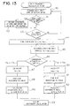
CPU 29, the position δ of the coordinate designator from the wire N producing the largest detection voltage can be calculated on the basis of the ratio (VN+1/VN) between the detection voltages of the wire N and adjacent wire N+1 respectively having the largest and the next largest values in the detection voltages of the wires, and then a coordinate point indicate of the coordinate designator can be calculated on the basis of the position δ. - The above calculation procedure will be explained by referring to a flowchart of Fig. 13. In the drawing, first, a detection signal is input from a wire in a
step 40 and it is judged in astep 41 whether or not the input signal is larger than a predetermined value. Determination of NO in thestep 41 causes control to proceed to astep 43. Determination of YES in thestep 41 causes control to go to astep 42 where the coordinate valus of the wire and the size of the detection signal are recorded in the memory and control goes to thestep 43. In thestep 43, it is judged whether or not detection of all the wires has been completed. Determination of NO in thestep 43 causes control to go back to thestep 40 to input the detection signal of the next wire. Determination of YES, on the other hand, causes control to proceed to astep 44 to find detection signals VN-1, VN, VN+1, ... which have been judged as having predetermined continuous values. In anext step 45, one of these detection signals having a maximum value, for example, the signal VN is determined. - Subsequently, comparison is made in a
next step 46 between the detection signals VN-1 and VN+1 of the wires N-1 and N+1 adjacent to the wire N which produced the maximum detection signal. When the comparison result satisfies a relation VN-1 > VN+1, control goes to astep 47 to calculate a value VN-1/VN. In anext step 48, a value δ is found by referencing a table (stored in the memory) having the characteristic as shown in Fig. 12. In anext step 49, the value δ is subtracted from the coordinate value of the wire N and then a coordinate point at which the coordinate designator is positioned is calculated. - If the comparison result in the
step 46 satisfies a relation VN+1 > VN-1, then control proceeds to astep 50 to calculate a value VN+1/VN. In anext step 51, the value δ is found by referencing the table according to the calculated value VN+1/VN. After this, in astep 52, the value δ is added to the coordinate value of the wire N to find a coordinate point indicative of the position of the coordinate designator. In astep 53, the coordinate calculation is completed. - Although the aforementioned coordinate calculation has been explained in connection with a single coordinate axis, the same explanation holds true for the coordinate calculation of the other coordiante axis with use of the similar flowchart.
- Explanation will be made as to yet a further embodiment. In the present embodiment, when circumferential magnetization is generated in a magnetic wire having a magnetostrictive coefficient of from zero to a negative value and when an exciting magnetic field caused by an exciting coil is applied to the magnetic wire, a pulse voltage is generated across the wire at the time that the circumferential magnetization is inverted. At this time, if an external magnetic field other than the exciting magnetic field is present, then the pulse voltage at the time of the magnetization reversal is influenced by both of the exciting magnetic field and the external magnetic field. Thus, when the exciting magnetic field is previously set at a predetermined value, the intensity of the external magnetic field can be detected. Further, in the case where a plurality of exciting coils are arranged along a magnetic wire so that a switch enables sequential change-over of the exciting coils, an external magnetic field in the vicinity of associated one of the exciting coils can be detected, whereby a magnetic image sensor can be realized.
- Provision of the circumferential magnetization to a magnetic wire having a magnetostrictive coefficient of zero to a negative value can be realized by providing a suitable twist to the magnetic wire to give it a twisting stress.
- In the event where provision of the circumferential magnetization to a magnetic wire having a magnetostrictive coefficient of zero to a negative value is realized by providing a twist to the magnetic wire, when the external magnetic field exceeds a predetermined value, this causes inversion of the magnetization, at which time a voltage proportional to -d/dt is generated, where denotes magnetic flux. Accordingly, an A.C. magnetic field is applied to the magnetic wire, a pulse voltage at the time of the magnetization inversion is developed across the magnetic wire. Under such a condition, if a magnetic field other than the magnetic field caused by the exciting coil in the vicinity of the magnetic wire is present, then a composite magnetic field of the both magnetic fields is applied to the magnetic wire so that the composite magnetic field causes inversion of the magnetization in the interior of the magnetic wire. In other words, the external magnetic field acts as a modulation signal when the exciting magnetic field is considered to be a carrier, and thus separate detection of the external magnetic field can be realized by processing the signal caused by the magnetization inversion. Detection of the external magnetic field can be attained with a high resolution by narrowing the range of the exciting magnetic field and this can be realized with use of a ferrite core wound by a winding.
Claims (13)
- A coordinate input device based on Matteucci effect, comprising:A magnetic wire matrix (18) made of a plurality of magnetic wires (1, 1') arranged as equi-spaced in X and Y directions;means (4, 49) for providing circumferential magnetization to said magnetic wires;a coordinate designator (2) for generating an A.C. magnetic field at its tip end;means (5, 7, 19-21, 23, 25-27) for detecting a Matteucci-effect voltage developed between both ends of a magnetic wire when said coordinate designator approaches said magnetic wires, andmeans (29) for determining a coordinate position of said coordinate designator on the basis of a coordinate position of at least one magnetic wire detected by said voltage detection means respectively in said X and Y directions.
- A device according to claim 1, wherein the circumferential magnetization means comprises means (4) for supplying a D.C. current to each of said magnetic wires.
- A device according to claim 1, wherein the magnetic wires are made of material having a magnetostrictive coefficient of zero to a negative value.
- A device according to claim 3, wherein the circumferential magnetization means comprises means (59) for applying a twist to said magnetic wire.
- A device according to claim 1, wherein the coordinate designator includes an A.C. power supply source (25) and an electromagnet for generating an A.C. magnetic field by an A.C. current from said A.C. power supply source.
- A device according to claim 1, further comprising A.C. high-impedance means (3) connected to at least one end of the magnetic wires for detecting said Matteucci-effect voltage.
- A device according to claim 1, wherein the Matteucci-effect voltage detection means detects a frequency component having a frequency which is twice a frequency of the A.C. magnetic field of said coordinate designator.
- A device according to claim 1, wherein each of the magnetic wires is made of go and return line paths (1, 1') disposed close to each other.
- A device according to claim 8, wherein an insulation means is provided to avoid electrical contact between the go and return line paths of the magnetic wire.
- A device according to claim 1, wherein the Matteucci-effect voltage detection means includes decoders (20, 21) each having a plurality of switching elements connected to one ends of said magnetic wires and means for sequentially turning ON and OFF said switching elements one after another, a wire selection circuit (23) for providing a control signal to the decoders for sequentially turning ON and OFF said switching elements, and circuits (19, 25, 26) commonly connected to the other ends of all of the magnetic wires for detecting said Matteucci-effect voltage.
- A device according to claim 10, wherein the voltage detection circuit includes a line (19) connected to the other ends of all said magnetic wires and detection circuits (25, 26) for detecting a magnitude of the Matteucci-effect voltage appearing on said line.
- A device according to claim 1, wherein the coordinate position determination means includes, with respect to each of said X and Y directions, means (45) for determining a coordinate position of one of the magnetic wires having the maximum one of the Matteucci-effect voltages detected across the magnetic wires, means (46) for comparing the voltages appearing across the two magnetic wires at both sides of and adjacent to the magnetic wire having the maximum voltage, and means (47-52) for calculating a coordinate position of the coordinate designator located between the two magnetic wires on the basis of the Matteucci-effect voltage of the magnetic wire having the larger one of the comparison voltages and the Matteucci-effect voltage of the magnetic wire having the maximum voltage.
- A device according to claim 12, wherein the coordinate position calculation means includes means (47, 50) for dividing the larger voltage (VN±1) by the maximum voltage (VN), means (48, 51) for finding a distance δ from a center of the magnetic wire indicative of said maximum voltage by referencing a table (Fig. 11) showing a relationship between the division value and said distance δ and previously stored in a memory, and means (49, 51) for calculating the coordinate position of the coordinate designator on the basis of the coordinate position of the magnetic wire indicative of the maximum voltage and the distance δ.
Applications Claiming Priority (10)
| Application Number | Priority Date | Filing Date | Title |
|---|---|---|---|
| JP32296490A JP2510781B2 (en) | 1990-11-28 | 1990-11-28 | Magnetic image sensor |
| JP32296590 | 1990-11-28 | ||
| JP322965/90 | 1990-11-28 | ||
| JP32296490 | 1990-11-28 | ||
| JP322964/90 | 1990-11-28 | ||
| JP32296590A JP3009213B2 (en) | 1990-11-28 | 1990-11-28 | Coordinate input device |
| JP892191 | 1991-01-29 | ||
| JP8921/91 | 1991-01-29 | ||
| JP3008921A JPH04252318A (en) | 1991-01-29 | 1991-01-29 | Coordinate input device |
| EP91120183A EP0488167B1 (en) | 1990-11-28 | 1991-11-26 | Magnetic detector based on Mateucci effect |
Related Parent Applications (2)
| Application Number | Title | Priority Date | Filing Date |
|---|---|---|---|
| EP91120183A Division EP0488167B1 (en) | 1990-11-28 | 1991-11-26 | Magnetic detector based on Mateucci effect |
| EP91120183.8 Division | 1991-11-26 |
Publications (2)
| Publication Number | Publication Date |
|---|---|
| EP0751398A1 EP0751398A1 (en) | 1997-01-02 |
| EP0751398B1 true EP0751398B1 (en) | 2001-01-31 |
Family
ID=27278252
Family Applications (3)
| Application Number | Title | Priority Date | Filing Date |
|---|---|---|---|
| EP91120183A Expired - Lifetime EP0488167B1 (en) | 1990-11-28 | 1991-11-26 | Magnetic detector based on Mateucci effect |
| EP95118295A Expired - Lifetime EP0706057B1 (en) | 1990-11-28 | 1991-11-26 | Magnetic image sensor using Matteucci effect |
| EP96113405A Expired - Lifetime EP0751398B1 (en) | 1990-11-28 | 1991-11-26 | Coordinate input device using Mateucci effect |
Family Applications Before (2)
| Application Number | Title | Priority Date | Filing Date |
|---|---|---|---|
| EP91120183A Expired - Lifetime EP0488167B1 (en) | 1990-11-28 | 1991-11-26 | Magnetic detector based on Mateucci effect |
| EP95118295A Expired - Lifetime EP0706057B1 (en) | 1990-11-28 | 1991-11-26 | Magnetic image sensor using Matteucci effect |
Country Status (4)
| Country | Link |
|---|---|
| US (2) | US5298689A (en) |
| EP (3) | EP0488167B1 (en) |
| KR (1) | KR960006091B1 (en) |
| DE (3) | DE69132101T2 (en) |
Families Citing this family (13)
| Publication number | Priority date | Publication date | Assignee | Title |
|---|---|---|---|---|
| JPH05233147A (en) * | 1992-02-21 | 1993-09-10 | Mitsubishi Electric Corp | Display incorporating type tablet |
| BE1007126A3 (en) * | 1992-06-24 | 1995-04-04 | Andre Albert Madelein Heerwegh | Method and device for reading of three-dimensional information. |
| US5920307A (en) * | 1995-02-21 | 1999-07-06 | Lucent Technologies, Inc. | System for directly sensing the orientation of a track ball |
| JP3091398B2 (en) * | 1995-09-14 | 2000-09-25 | 科学技術振興事業団 | Magnetic-impedance element and method of manufacturing the same |
| US6396005B2 (en) | 1998-06-15 | 2002-05-28 | Rodgers Technology Center, Inc. | Method and apparatus for diminishing grid complexity in a tablet |
| WO2003105072A2 (en) * | 2002-06-05 | 2003-12-18 | Synaptics (Uk) Limited | Signal transfer method and apparatus |
| JP4527752B2 (en) * | 2007-06-22 | 2010-08-18 | 日立オムロンターミナルソリューションズ株式会社 | Paper sheet identification device and sensor section thereof |
| EP2690450B1 (en) * | 2012-07-27 | 2014-07-09 | ABB Technology AG | A device for measuring the direct component of alternating current |
| DE102014200461B4 (en) | 2014-01-14 | 2016-01-14 | Schaeffler Technologies AG & Co. KG | Arrangement for measuring a force or a torque on a machine element |
| DE102014214249B3 (en) | 2014-07-22 | 2015-09-10 | Schaeffler Technologies AG & Co. KG | Machine element and arrangement for measuring a force or a moment and method for producing the machine element |
| DE102014219336B3 (en) | 2014-09-24 | 2016-01-21 | Schaeffler Technologies AG & Co. KG | Method and arrangement for measuring a force or a moment with a plurality of magnetic field sensors |
| DE102015206152B3 (en) | 2015-04-07 | 2016-07-07 | Schaeffler Technologies AG & Co. KG | 1 - 12An arrangement and method for non-contact measurement of a moment on a machine element |
| CN107728866A (en) * | 2017-09-18 | 2018-02-23 | 安徽工程大学 | A kind of Computer Aided Put-Together Drawing System |
Family Cites Families (9)
| Publication number | Priority date | Publication date | Assignee | Title |
|---|---|---|---|---|
| FR2087205A5 (en) * | 1970-05-11 | 1971-12-31 | Dassault Electronique | |
| US4374403A (en) * | 1979-06-27 | 1983-02-15 | Matsushita Electric Industrial Co., Ltd. | Magnetic recording and reproducing system |
| US4418242A (en) * | 1980-03-04 | 1983-11-29 | Fujitsu Limited | Coordinate reading apparatus |
| JPS58117718A (en) * | 1981-12-30 | 1983-07-13 | Aisin Seiki Co Ltd | Pulse generator |
| JPS6170628A (en) | 1984-09-13 | 1986-04-11 | Hitachi Metals Ltd | Element for data tablet |
| KR930011886B1 (en) * | 1984-12-28 | 1993-12-22 | 가부시기가이샤 와꼬무 | Position detecting device |
| JPS6326720A (en) * | 1986-07-18 | 1988-02-04 | Nippon Denki Shijiyou Kaihatsu Kk | Detecting device for frequency connecting position |
| US4939459A (en) * | 1987-12-21 | 1990-07-03 | Tdk Corporation | High sensitivity magnetic sensor |
| US4963703A (en) * | 1989-07-18 | 1990-10-16 | Numonics Corporation | Coordinate determining device using spatial filters |
-
1991
- 1991-11-26 DE DE69132101T patent/DE69132101T2/en not_active Expired - Fee Related
- 1991-11-26 EP EP91120183A patent/EP0488167B1/en not_active Expired - Lifetime
- 1991-11-26 KR KR1019910021190A patent/KR960006091B1/en not_active IP Right Cessation
- 1991-11-26 DE DE69127530T patent/DE69127530T2/en not_active Expired - Fee Related
- 1991-11-26 DE DE69132528T patent/DE69132528T2/en not_active Expired - Fee Related
- 1991-11-26 EP EP95118295A patent/EP0706057B1/en not_active Expired - Lifetime
- 1991-11-26 US US07/797,923 patent/US5298689A/en not_active Expired - Lifetime
- 1991-11-26 EP EP96113405A patent/EP0751398B1/en not_active Expired - Lifetime
-
1993
- 1993-09-10 US US08/118,764 patent/US5446377A/en not_active Expired - Lifetime
Also Published As
| Publication number | Publication date |
|---|---|
| EP0706057B1 (en) | 2000-04-05 |
| EP0706057A2 (en) | 1996-04-10 |
| DE69132101D1 (en) | 2000-05-11 |
| DE69132528D1 (en) | 2001-03-08 |
| US5298689A (en) | 1994-03-29 |
| KR960006091B1 (en) | 1996-05-08 |
| US5446377A (en) | 1995-08-29 |
| DE69132101T2 (en) | 2000-09-28 |
| EP0751398A1 (en) | 1997-01-02 |
| DE69127530D1 (en) | 1997-10-09 |
| DE69127530T2 (en) | 1998-02-12 |
| DE69132528T2 (en) | 2001-06-13 |
| EP0488167A2 (en) | 1992-06-03 |
| KR920010310A (en) | 1992-06-26 |
| EP0488167A3 (en) | 1994-03-02 |
| EP0488167B1 (en) | 1997-09-03 |
| EP0706057A3 (en) | 1996-05-01 |
Similar Documents
| Publication | Publication Date | Title |
|---|---|---|
| EP0751398B1 (en) | Coordinate input device using Mateucci effect | |
| US4603365A (en) | Magnetic detection apparatus | |
| US6124708A (en) | Position detection using a spaced apart array of magnetic field generators and plural sensing loop circuits offset from one another in the measurement direction | |
| EP0607694B1 (en) | Cordless digitizer | |
| EP0187372A2 (en) | Position detecting device | |
| US4554409A (en) | Method of electromagnetically reading coordinate data | |
| GB2034053A (en) | Magneto resistive displacement sensors | |
| JPH08249105A (en) | Sensor coil pattern and coordinate input device | |
| JP3367230B2 (en) | Position detection device | |
| US4298772A (en) | Coordinate reader using adjustable magnetostrictive oscillations | |
| JPH05340709A (en) | Three-dimensional shape measuring instrument | |
| JP3037380B2 (en) | Magnetic encoder | |
| JPS5856912B2 (en) | 2D magnetic scale device | |
| JPH07190804A (en) | Magnetic-field measuring device having magnetoresistance type sensor | |
| US4806708A (en) | Coordinate determining device and method of determining X-Y coordinate position | |
| US4996392A (en) | Superconductor magnetic image detection device | |
| KR960004556B1 (en) | Coordinates input device using mateuchi effect | |
| JP3379258B2 (en) | Absolute encoder | |
| JPH0266479A (en) | Magnetoresistance effect element | |
| WO1997014014A1 (en) | Inductive device for determining measures and positions of measuring objects of electrically conductive material | |
| Green | Search coils | |
| JP3047567B2 (en) | Orientation sensor | |
| JP2611642B2 (en) | Coordinate position detector | |
| JP2576136B2 (en) | Magnetic direction measurement device | |
| JPS58222772A (en) | Position detector for linear pulse motor |
Legal Events
| Date | Code | Title | Description |
|---|---|---|---|
| PUAI | Public reference made under article 153(3) epc to a published international application that has entered the european phase |
Free format text: ORIGINAL CODE: 0009012 |
|
| AC | Divisional application: reference to earlier application |
Ref document number: 488167 Country of ref document: EP |
|
| AK | Designated contracting states |
Kind code of ref document: A1 Designated state(s): DE FR GB |
|
| 17P | Request for examination filed |
Effective date: 19961115 |
|
| 17Q | First examination report despatched |
Effective date: 19990114 |
|
| GRAG | Despatch of communication of intention to grant |
Free format text: ORIGINAL CODE: EPIDOS AGRA |
|
| GRAG | Despatch of communication of intention to grant |
Free format text: ORIGINAL CODE: EPIDOS AGRA |
|
| GRAH | Despatch of communication of intention to grant a patent |
Free format text: ORIGINAL CODE: EPIDOS IGRA |
|
| GRAH | Despatch of communication of intention to grant a patent |
Free format text: ORIGINAL CODE: EPIDOS IGRA |
|
| GRAA | (expected) grant |
Free format text: ORIGINAL CODE: 0009210 |
|
| AC | Divisional application: reference to earlier application |
Ref document number: 488167 Country of ref document: EP |
|
| AK | Designated contracting states |
Kind code of ref document: B1 Designated state(s): DE FR GB |
|
| REF | Corresponds to: |
Ref document number: 69132528 Country of ref document: DE Date of ref document: 20010308 |
|
| ET | Fr: translation filed | ||
| PLBE | No opposition filed within time limit |
Free format text: ORIGINAL CODE: 0009261 |
|
| STAA | Information on the status of an ep patent application or granted ep patent |
Free format text: STATUS: NO OPPOSITION FILED WITHIN TIME LIMIT |
|
| REG | Reference to a national code |
Ref country code: GB Ref legal event code: IF02 |
|
| 26N | No opposition filed | ||
| PGFP | Annual fee paid to national office [announced via postgrant information from national office to epo] |
Ref country code: DE Payment date: 20081126 Year of fee payment: 18 |
|
| PGFP | Annual fee paid to national office [announced via postgrant information from national office to epo] |
Ref country code: FR Payment date: 20081017 Year of fee payment: 18 |
|
| PGFP | Annual fee paid to national office [announced via postgrant information from national office to epo] |
Ref country code: GB Payment date: 20081021 Year of fee payment: 18 |
|
| GBPC | Gb: european patent ceased through non-payment of renewal fee |
Effective date: 20091126 |
|
| REG | Reference to a national code |
Ref country code: FR Ref legal event code: ST Effective date: 20100730 |
|
| PG25 | Lapsed in a contracting state [announced via postgrant information from national office to epo] |
Ref country code: FR Free format text: LAPSE BECAUSE OF NON-PAYMENT OF DUE FEES Effective date: 20091130 |
|
| PG25 | Lapsed in a contracting state [announced via postgrant information from national office to epo] |
Ref country code: DE Free format text: LAPSE BECAUSE OF NON-PAYMENT OF DUE FEES Effective date: 20100601 |
|
| PG25 | Lapsed in a contracting state [announced via postgrant information from national office to epo] |
Ref country code: GB Free format text: LAPSE BECAUSE OF NON-PAYMENT OF DUE FEES Effective date: 20091126 |