EP0749673B1 - Fabrication multilayer combined rigid/flex printed circuit board - Google Patents
Fabrication multilayer combined rigid/flex printed circuit board Download PDFInfo
- Publication number
- EP0749673B1 EP0749673B1 EP94919968A EP94919968A EP0749673B1 EP 0749673 B1 EP0749673 B1 EP 0749673B1 EP 94919968 A EP94919968 A EP 94919968A EP 94919968 A EP94919968 A EP 94919968A EP 0749673 B1 EP0749673 B1 EP 0749673B1
- Authority
- EP
- European Patent Office
- Prior art keywords
- flexible
- printed circuit
- rigid
- layer
- insulator
- Prior art date
- Legal status (The legal status is an assumption and is not a legal conclusion. Google has not performed a legal analysis and makes no representation as to the accuracy of the status listed.)
- Expired - Lifetime
Links
Images



Classifications
-
- H—ELECTRICITY
- H05—ELECTRIC TECHNIQUES NOT OTHERWISE PROVIDED FOR
- H05K—PRINTED CIRCUITS; CASINGS OR CONSTRUCTIONAL DETAILS OF ELECTRIC APPARATUS; MANUFACTURE OF ASSEMBLAGES OF ELECTRICAL COMPONENTS
- H05K3/00—Apparatus or processes for manufacturing printed circuits
- H05K3/46—Manufacturing multilayer circuits
- H05K3/4688—Composite multilayer circuits, i.e. comprising insulating layers having different properties
- H05K3/4691—Rigid-flexible multilayer circuits comprising rigid and flexible layers, e.g. having in the bending regions only flexible layers
-
- H—ELECTRICITY
- H05—ELECTRIC TECHNIQUES NOT OTHERWISE PROVIDED FOR
- H05K—PRINTED CIRCUITS; CASINGS OR CONSTRUCTIONAL DETAILS OF ELECTRIC APPARATUS; MANUFACTURE OF ASSEMBLAGES OF ELECTRICAL COMPONENTS
- H05K2201/00—Indexing scheme relating to printed circuits covered by H05K1/00
- H05K2201/01—Dielectrics
- H05K2201/0183—Dielectric layers
- H05K2201/0187—Dielectric layers with regions of different dielectrics in the same layer, e.g. in a printed capacitor for locally changing the dielectric properties
-
- H—ELECTRICITY
- H05—ELECTRIC TECHNIQUES NOT OTHERWISE PROVIDED FOR
- H05K—PRINTED CIRCUITS; CASINGS OR CONSTRUCTIONAL DETAILS OF ELECTRIC APPARATUS; MANUFACTURE OF ASSEMBLAGES OF ELECTRICAL COMPONENTS
- H05K2201/00—Indexing scheme relating to printed circuits covered by H05K1/00
- H05K2201/09—Shape and layout
- H05K2201/09009—Substrate related
- H05K2201/09109—Locally detached layers, e.g. in multilayer
-
- Y—GENERAL TAGGING OF NEW TECHNOLOGICAL DEVELOPMENTS; GENERAL TAGGING OF CROSS-SECTIONAL TECHNOLOGIES SPANNING OVER SEVERAL SECTIONS OF THE IPC; TECHNICAL SUBJECTS COVERED BY FORMER USPC CROSS-REFERENCE ART COLLECTIONS [XRACs] AND DIGESTS
- Y10—TECHNICAL SUBJECTS COVERED BY FORMER USPC
- Y10S—TECHNICAL SUBJECTS COVERED BY FORMER USPC CROSS-REFERENCE ART COLLECTIONS [XRACs] AND DIGESTS
- Y10S428/00—Stock material or miscellaneous articles
- Y10S428/901—Printed circuit
-
- Y—GENERAL TAGGING OF NEW TECHNOLOGICAL DEVELOPMENTS; GENERAL TAGGING OF CROSS-SECTIONAL TECHNOLOGIES SPANNING OVER SEVERAL SECTIONS OF THE IPC; TECHNICAL SUBJECTS COVERED BY FORMER USPC CROSS-REFERENCE ART COLLECTIONS [XRACs] AND DIGESTS
- Y10—TECHNICAL SUBJECTS COVERED BY FORMER USPC
- Y10T—TECHNICAL SUBJECTS COVERED BY FORMER US CLASSIFICATION
- Y10T156/00—Adhesive bonding and miscellaneous chemical manufacture
- Y10T156/10—Methods of surface bonding and/or assembly therefor
- Y10T156/1052—Methods of surface bonding and/or assembly therefor with cutting, punching, tearing or severing
- Y10T156/1062—Prior to assembly
- Y10T156/1075—Prior to assembly of plural laminae from single stock and assembling to each other or to additional lamina
-
- Y—GENERAL TAGGING OF NEW TECHNOLOGICAL DEVELOPMENTS; GENERAL TAGGING OF CROSS-SECTIONAL TECHNOLOGIES SPANNING OVER SEVERAL SECTIONS OF THE IPC; TECHNICAL SUBJECTS COVERED BY FORMER USPC CROSS-REFERENCE ART COLLECTIONS [XRACs] AND DIGESTS
- Y10—TECHNICAL SUBJECTS COVERED BY FORMER USPC
- Y10T—TECHNICAL SUBJECTS COVERED BY FORMER US CLASSIFICATION
- Y10T156/00—Adhesive bonding and miscellaneous chemical manufacture
- Y10T156/17—Surface bonding means and/or assemblymeans with work feeding or handling means
- Y10T156/1798—Surface bonding means and/or assemblymeans with work feeding or handling means with liquid adhesive or adhesive activator applying means
-
- Y—GENERAL TAGGING OF NEW TECHNOLOGICAL DEVELOPMENTS; GENERAL TAGGING OF CROSS-SECTIONAL TECHNOLOGIES SPANNING OVER SEVERAL SECTIONS OF THE IPC; TECHNICAL SUBJECTS COVERED BY FORMER USPC CROSS-REFERENCE ART COLLECTIONS [XRACs] AND DIGESTS
- Y10—TECHNICAL SUBJECTS COVERED BY FORMER USPC
- Y10T—TECHNICAL SUBJECTS COVERED BY FORMER US CLASSIFICATION
- Y10T428/00—Stock material or miscellaneous articles
- Y10T428/24—Structurally defined web or sheet [e.g., overall dimension, etc.]
- Y10T428/24802—Discontinuous or differential coating, impregnation or bond [e.g., artwork, printing, retouched photograph, etc.]
- Y10T428/24917—Discontinuous or differential coating, impregnation or bond [e.g., artwork, printing, retouched photograph, etc.] including metal layer
Definitions
- the present invention relates to the fabrication of multilayer combined rigid and flex printed circuits having flexible printed circuits extending from the rigid board.
- the present invention relates to an improved process for the fabrication of a novel multilayer combined rigid and flex printed circuits, wherein the flex section has improved flexibility, thereby providing a rigid flex circuit with optimum flexibility in the connecting flex sections.
- a rigid flex stacked printed circuit board includes flexible printed circuit cables extending from the periphery of the rigid section or sections.
- the rigid portions of the flex cables are typically used as sites for electronic components or mechanical hardware. It is important to note that the copper conductor in each plane or layer is fabricated from one continuous sheet of copper foil.
- the '461 patent reported on a novel process to provide a rigid section incorporating insulator materials which, when subjected to elevated temperatures, did not expand in the Z direction to cause difficulties, including delamination and cracking of plated copper barrels. Stated another way, in the '461 patent,the materials causing undesirable expansion in the Z direction in the multilayer rigid section of the board, and the materials absorbing excessive amounts of moisture, such as acrylic adhesives and Kapton, were eliminated from the boards rigid section.
- the process for fabrication of the rigid flex printed circuits has remained limited to the fabrication of a multilayer combined rigid and flex printed circuit board wherein two circuit boards are always prepared from a basestock composition, and remain attached to one another via the prepreg.
- the process of fabrication according to the teachings of the prior art begin with the step of laminating two conductor layers (i.e. copper layers) to a single insulator layer (prepreg) followed by imaging and etching. Accordingly if one of the two bonded conductor layers was somehow improperly imaged, it was necessary to discard the entire lamination.
- the basestock could be imaged and processed in the usual manner, such that cutting the edges of the basestock material, after imaging, at a location internal to the basestock, provided a cut into the release layer, thereby allowing for separation of the two individual imaged copper layers and their supporting prepreg, along with the removal of said release material.
- a layered rigid flex circuit with enhanced flexibility, that is comprised of a laminated double sided base stock composite with a flexible core, two additional insulator prepreg sheets positioned on both sides of the basestock, wherein cutouts are made in said additional insulator prepreg sheets at a region proximate to the flexible core, said cutout regions being filled with a flexible layer of Kapton affixed to the basestock composite by a suitable adhesive, and abutting and overlapping the edges of the cutout, whereupon stacking of the laminate so produced results in the formation of a hollow region as between the flexible Kapton layers, therein resulting in a rigid flex circuit with improved and optimum flexibility in the flex section.
- This invention describes a multilayer rigid flex printed circuit board, wherein the board laminate comprises a double-sided basestock composite, formed by laminating two conducting sheets to an insulating layer, said insulator layer containing a flexible core, a second insulator layer affixed to each side of the basestock, said insulator having a cutout region proximate to the flexible core of the basestock composite, a flexible layer affixed to said cutout regions with an adhesive, wherein said flexible layer contacts the conducting layers and abuts and overlaps a portion of the second insulator layer such that upon stacking of the board laminate a hollow region is produced as between the stacked laminate sections the hollow region being aligned vertically within the flexible core.
- the board laminate comprises a double-sided basestock composite, formed by laminating two conducting sheets to an insulating layer, said insulator layer containing a flexible core, a second insulator layer affixed to each side of the basestock, said insulator having a cutout region proximate
- the conducting sheets are copper sheets, preferably of 28.35 to 56.7 gram copper (one or two ounce copper), the flexible core and the flexible layers are preferably polyimide, such as Kapton (trademark), the insulator layers preferably comprised of one or two fiberglass sheets impregnated with an adhesive, preferably an epoxy or polyimide (commonly referred to as a prepreg) and the polyimide is affixed to the laminate by an acrylic type adhesive.
- an adhesive preferably an epoxy or polyimide (commonly referred to as a prepreg) and the polyimide is affixed to the laminate by an acrylic type adhesive.
- the present invention describes a process of fabricating a rigid flex printed circuit as defined in claim 8.
- the basestock composite 10 is shown to comprise two copper conducting sheets 12 and 14, for example, one or two ounce copper, bonded to insulator layers 16 and 18 comprised of fiberglass sheets impregnated with an adhesive such as epoxy, and commonly referred to as a prepreg.
- the flexible core 20 for example, a polyimide film such as Kapton, affixed to the prepreg 12 and 18 by an acrylic-type adhesive.
- a pair of conducting sheets or layers 12 and 14 are laminated to the opposite surfaces of insulating layers 16 and 18, containing flexible core 20.
- the basestock composite 10 comprising a pair of conducting sheets has sufficient planarity and rigidity to permit handling and further processing thereof, and in particular, imaging to form conductor patterns.
- the basestock composite which has been imaged and etched to form conductor patterns are first treated to enhance bondability of another epoxy prepreg to the copper, shown at 24 and 26, by the black oxide process typically used in the rigid board field, or by way of a double treated foil.
- prepreg 24 and 26 have cutout regions which contain a flexible insulator film of Kapton, shown at 28 and 30, covered with a layer of suitable adhesive which provides excellent bonding of Kapton to copper.
- the flexible layer of Kapton at 28 and 30 contacts the conducting layers and abuts and overlaps a portion of the second insulating layers 24 and 26.
- the insulator layers such as Kapton and acrylic adhesive afford flexibility and tear resistance characteristics to the flex sections.
- the Kapton and adhesive can be replaced with a photoimagable solder mask.
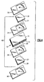
- Fig. 3 the laminate of Fig. 2 has been stacked such that a hollow region 32 can be seen as between the stacked laminate sections.
- the stacking can be readily achieved by laminating through the use of another prepreg sheet shown at 34.
- the formation of the multilayer rigid flex printed circuits begins with supplying the basestock composite 10 (which contains flexible core 20, as shown more clearly in Fig. 1) followed by an initial processing step which includes treating the exposed copper conductor patterns 12 and 14 to enhance bondability of another epoxy prepreg to the copper, for example, by the black oxide process typically used in the rigid board field, or by way of a double treated foil.
- the flexible core indicated generally at 20 is of a cross-sectional size that is substantially the same as that of the subsequent layers of flexible layers to be attached.
- One additional insulator prepreg sheets 24, having cutout 36, is positioned on one side of the base stock 10.
- a similar sheet of Kapton 28 covered with a layer of adhesive 27 is located on the other side of the glass sheet 26.
- Insulator layers such as Kapton and acrylic adhesive afford flexibility and tear resistance characteristics to the flex sections, as discussed in connection with Figs. 6 and 7.
- the Kapton 28 and adhesive 27 can be replaced with a photoimagable solder mask.
- the Kapton sheets 28 and 30 and their associated adhesive layers 27 and 31 are slightly longer than the length of the cutouts 36 and 38 (Fig. 4) in the glass layers to overlap slightly the sheet 24 and 26 by, for example 0,127cm (0.050 inch).
- the sandwich formed by the foregoing sheets is then laminated together to provide the printed circuit structure 40 shown in Figs. 4 and 5. Note that in the interests of clarity, the sides of the cutouts are not shown in Fig. 7.
- a number of the printed circuits 40 are stacked in proper registration with epoxy impregnated fiberglass layers 42 (Fig. 7) positioned between, for example, seven of the circuits 40.
- epoxy impregnated fiberglass layers 42 Fig. 7
- cutouts 48 in the prepreg sheets 50 are slightly longer than the cutouts 36 (Fig. 4) and coextensive with the Kapton layers 28 and 30 so that the Kapton layers 28 and 30 abut the edges of the sheets 48, as shown in Fig. 6.
- the layers are laminated to provide, in this example, a nine layer rigid flex circuit (the outer caps add in this example one layer per cap), and holes are then drilled at appropriate pads 52 to interconnect desired conductors 54.
- the holes are then desmeared by a suitable process, for example, exposing them to appropriate cleaning chemicals to expose fully the copper conductors, a rapid process due to the absence of any adhesives or insulating material resistant to such chemicals, such as acrylics and Kapton, in the rigid circuit portion.
- plasma desmearing techniques can be used instead of chemical cleaning.
- the holes are then plated through to interconnect desired conductors 54, a portion of a plated-through barrel 56 being shown in broken lines in Fig. 6, because it will not be formed until after lamination of the circuits 40 with the prepreg layers 50.
- Fig. 7 which shows somewhat diagrammatically a rigid flex circuit 58 with the plated through holes 56 enlarged, in the interests of clarity, flex cables 60 coextensive with the rigid and flex sections, and extending between the rigid sections 62 and 64 for suitably connecting the printed circuits.
- upper and lower caps are laminated to the circuits 40 in the rigid board area 62 only.
- Such caps typically are fabricated using polyimide glass or epoxy glass copper-clad laminates. Copper conductor circuits can be formed on one or both sides of the caps, as desired.
- an insulator material i.e., layers of fiberglass and adhesive, such as epoxy, which have characteristics or properties which allow the rigid board portion to relieve stresses, caused by heating, in the board, delamination of the circuits and cracking of the plated through barrels is prevented when the board, or portions thereof, is subjected to elevated temperatures.
- the rigid board 62 does not contain troublesome materials, such as acrylic adhesive and Kapton, having high expansion rates and moisture absorption properties, because the flex cable sections including Kapton and acrylic adhesive only extend to but not substantially into the rigid section.
- Kapton and acrylic layers could extend an insubstantial distance into the rigid section without causing undue problems.
- subjecting the inventive circuits to hot solder reflow and elevated temperatures will not cause differential expansion and contraction leading to cracking of the copper plated through barrels 56 or delamination of the layers.
- expended baking times at temperatures on the order of 121°C (250°F)., often as long as 48 hours, to remove moisture, are avoided.
- the invention enables the successful fabrication of multilayer rigid flex boards having a great number of conductor layers, the invention also provides excellent multilayer rigid flex boards having fewer layers, for example, on the order of as few as four conductor layers.
- imaging and connection of the conductors of the circuits may be accomplished by covering the whole board with a layer of photoimagable solder mask to permit the whole board to be processed at once.
- this greatly reduces the costs of performing this processing step, and thus, reduces the overall cost of the resulting board.
- Other modifications are also possible.
Landscapes
- Engineering & Computer Science (AREA)
- Manufacturing & Machinery (AREA)
- Microelectronics & Electronic Packaging (AREA)
- Production Of Multi-Layered Print Wiring Board (AREA)
- Structure Of Printed Boards (AREA)
Abstract
Description
- The present invention relates to the fabrication of multilayer combined rigid and flex printed circuits having flexible printed circuits extending from the rigid board. In particular, the present invention relates to an improved process for the fabrication of a novel multilayer combined rigid and flex printed circuits, wherein the flex section has improved flexibility, thereby providing a rigid flex circuit with optimum flexibility in the connecting flex sections.
- Techniques for making multilayer rigid flex printed circuit boards are well known in the art. One early example of the prior art is disclosed in U.S. Patent No. 3,409,732, assigned to the Assignee of the present application and whose teachings are incorporated by reference. Typically a rigid flex stacked printed circuit board includes flexible printed circuit cables extending from the periphery of the rigid section or sections. The rigid portions of the flex cables are typically used as sites for electronic components or mechanical hardware. It is important to note that the copper conductor in each plane or layer is fabricated from one continuous sheet of copper foil.
- With improvements in electronic technology, there has been a constant need for advances in electronic packaging. This need has led to more complex multilayer rigid flex printed circuit boards with many boards now using up to twenty-five, or even more, layers of circuitry. However, severe problems developed when the rigid circuit portions included many layers of conductors and holes plated through with copper to provide conductor barrels connecting the conductor layers.
- One particular problem, reported on and discussed in U.S. Patent No. 4,800,461, assigned to the assignee of the present Application, and whose teachings are incorporated by reference, described the fact that in multilayer rigid flex boards which included insulator materials such as acrylic adhesive and Kapton (Kapton is a trademark of E.I. duPont de Nemours and Company Inc. for polyimide film), the insulating materials placed a "Z-axis" stress on plated through holes. The coefficient of thermal expansion, it was reported, of the acrylic adhesive (Z-axis expansion) was the dominate influence. It was observed that because of the amount of acrylic required in many multilayer rigid flex applications, all plated through holes are stressed, with many cracking, making the boards unusable.
- To overcome this problem, the '461 patent reported on a novel process to provide a rigid section incorporating insulator materials which, when subjected to elevated temperatures, did not expand in the Z direction to cause difficulties, including delamination and cracking of plated copper barrels. Stated another way, in the '461 patent,the materials causing undesirable expansion in the Z direction in the multilayer rigid section of the board, and the materials absorbing excessive amounts of moisture, such as acrylic adhesives and Kapton, were eliminated from the boards rigid section.
- However, although the '461 patent was extremely successful in addressing the various problems recited therein, and in particular, the problem of thermal stresses described above, the process for fabrication of the rigid flex printed circuits has remained limited to the fabrication of a multilayer combined rigid and flex printed circuit board wherein two circuit boards are always prepared from a basestock composition, and remain attached to one another via the prepreg. In other words, the process of fabrication according to the teachings of the prior art begin with the step of laminating two conductor layers (i.e. copper layers) to a single insulator layer (prepreg) followed by imaging and etching. Accordingly if one of the two bonded conductor layers was somehow improperly imaged, it was necessary to discard the entire lamination.
- In order to solve the above mentioned problem, as reported on and discussed in PCT/US93/11684, filed December 2, 1993, assigned to the assignee of the present application, and whose teachings are incorporated by reference, a process for the fabrication by a novel process and from a novel basestock composite was reported, wherein two copper sheets were laminated to a prepreg and in-between said laminated copper sheets was placed a release material that was not coextensive with the borders of the prepreg. Accordingly, the basestock could be imaged and processed in the usual manner, such that cutting the edges of the basestock material, after imaging, at a location internal to the basestock, provided a cut into the release layer, thereby allowing for separation of the two individual imaged copper layers and their supporting prepreg, along with the removal of said release material.
- Documents US-A-4800461 and US-A-4687695 disclose a multilayer rigid flex printed circuit board, wherein the board laminate comprises a double-side base stock composite, formed by laminating two conducting sheets to an insulator layer.
- However, while the above solutions to certain problems in multilayer combined rigid and flex printed circuits each put to rest some longstanding problems in circuit manufacture, none of the described solutions addressed the problem of preparing a rigid flex circuit wherein maximum flexibility was developed in the flexible section of the circuit.
- Accordingly, it is an object of this invention to provide a novel rigid flex printed circuit, and process for its fabrication, that improves the ductility or flexibility of the flex section.
- It is also an object of this invention to provide a novel rigid flex printed circuit, and process for its fabrication, wherein flexible insulating layers, preferably made of Kapton film, are positioned and configured in the circuit such that a hollow region is defined by said layers of Kapton, which hollow region also serves to enhance the flexibility of the rigid flex circuit so produced.
- Finally, it is a particular object of this invention to disclose a layered rigid flex circuit, with enhanced flexibility, that is comprised of a laminated double sided base stock composite with a flexible core, two additional insulator prepreg sheets positioned on both sides of the basestock, wherein cutouts are made in said additional insulator prepreg sheets at a region proximate to the flexible core, said cutout regions being filled with a flexible layer of Kapton affixed to the basestock composite by a suitable adhesive, and abutting and overlapping the edges of the cutout, whereupon stacking of the laminate so produced results in the formation of a hollow region as between the flexible Kapton layers, therein resulting in a rigid flex circuit with improved and optimum flexibility in the flex section.
- This invention describes a multilayer rigid flex printed circuit board, wherein the board laminate comprises a double-sided basestock composite, formed by laminating two conducting sheets to an insulating layer, said insulator layer containing a flexible core, a second insulator layer affixed to each side of the basestock, said insulator having a cutout region proximate to the flexible core of the basestock composite, a flexible layer affixed to said cutout regions with an adhesive, wherein said flexible layer contacts the conducting layers and abuts and overlaps a portion of the second insulator layer such that upon stacking of the board laminate a hollow region is produced as between the stacked laminate sections the hollow region being aligned vertically within the flexible core. In an exemplary embodiment of the invention, the conducting sheets are copper sheets, preferably of 28.35 to 56.7 gram copper (one or two ounce copper), the flexible core and the flexible layers are preferably polyimide, such as Kapton (trademark), the insulator layers preferably comprised of one or two fiberglass sheets impregnated with an adhesive, preferably an epoxy or polyimide (commonly referred to as a prepreg) and the polyimide is affixed to the laminate by an acrylic type adhesive.
- In process form, the present invention describes a process of fabricating a rigid flex printed circuit as defined in claim 8.
- The foregoing and other features and advantages of the present invention will be more readily understood and will become apparent from the following detailed description taken in conjunction with the drawings, in which:
- Fig. 1 is an exploded view of the novel basestock composite, containing a Kapton core.
- Fig. 2 is an exploded view of the novel basestock composite covered with a second insulator prepreg layer and a cutout region containing a Kapton/acrylic covering.
- Fig. 3 is an exploded view of a stacked laminate of Fig. 2.
- Fig. 4 is an exploded view of the sheet materials used to form the layers of structures forming inventive rigid flex circuit;
- Fig. 5 is a view in perspective of the layers of Fig. 4 following lamination and certain processing steps;
- Fig. 6 is a cross-section taken along view line 3-3 in Fig. 5 and enlarged in the interest of clarity; and
- Fig. 7 is a perspective view diagrammatically showing the inventive rigid flex circuits following lamination and other processing steps of the structures shown in Figs. 5 and 6.
-
- In the first exemplary embodiment of the invention shown in Fig. 1, the
basestock composite 10 is shown to comprise twocopper conducting sheets insulator layers flexible core 20, for example, a polyimide film such as Kapton, affixed to theprepreg base stock composite 10, a pair of conducting sheets orlayers insulating layers flexible core 20. Thebasestock composite 10 comprising a pair of conducting sheets has sufficient planarity and rigidity to permit handling and further processing thereof, and in particular, imaging to form conductor patterns. - Turning now to Fig. 2, the basestock composite which has been imaged and etched to form conductor patterns are first treated to enhance bondability of another epoxy prepreg to the copper, shown at 24 and 26, by the black oxide process typically used in the rigid board field, or by way of a double treated foil. In addition, prepreg 24 and 26 have cutout regions which contain a flexible insulator film of Kapton, shown at 28 and 30, covered with a layer of suitable adhesive which provides excellent bonding of Kapton to copper. As shown in Fig. 2, the flexible layer of Kapton at 28 and 30 contacts the conducting layers and abuts and overlaps a portion of the second
insulating layers - Turning now to Fig. 3, the laminate of Fig. 2 has been stacked such that a
hollow region 32 can be seen as between the stacked laminate sections. The stacking can be readily achieved by laminating through the use of another prepreg sheet shown at 34. - In an exemplary embodiment of the invention shown in Figs. 4-7, the formation of the multilayer rigid flex printed circuits begins with supplying the basestock composite 10 (which contains
flexible core 20, as shown more clearly in Fig. 1) followed by an initial processing step which includes treating the exposedcopper conductor patterns insulator prepreg sheets 24, havingcutout 36, is positioned on one side of thebase stock 10. A flexible insulator of Kapton 30, covered with a layer ofsuitable adhesive 31, for example, an acrylic adhesive which provides excellent bonding of Kapton to copper, is positioned on one side of theglass sheet 24. A similar sheet ofKapton 28 covered with a layer ofadhesive 27 is located on the other side of theglass sheet 26. Insulator layers such as Kapton and acrylic adhesive afford flexibility and tear resistance characteristics to the flex sections, as discussed in connection with Figs. 6 and 7. Alternatively, the Kapton 28 and adhesive 27 can be replaced with a photoimagable solder mask. - As shown in Fig. 6, the
Kapton sheets adhesive layers cutouts 36 and 38 (Fig. 4) in the glass layers to overlap slightly thesheet circuit structure 40 shown in Figs. 4 and 5. Note that in the interests of clarity, the sides of the cutouts are not shown in Fig. 7. - After lamination processing, a number of the printed
circuits 40 are stacked in proper registration with epoxy impregnated fiberglass layers 42 (Fig. 7) positioned between, for example, seven of thecircuits 40. For clarity, only two of the printedcircuit structures 40 are shown with theupper circuit 40 illustrated diagrammatically and broken away. - Note that
cutouts 48 in theprepreg sheets 50 are slightly longer than the cutouts 36 (Fig. 4) and coextensive with theKapton layers Kapton layers sheets 48, as shown in Fig. 6. - Prior to stacking the
circuits 40, it is desirable to cut the flex cables, shown in Fig. 7, that extend through the cutout areas, to simplify the final construction of the rigid flex printed circuit structure. - After stacking seven of the
circuits 40 with appropriate outer caps, the layers are laminated to provide, in this example, a nine layer rigid flex circuit (the outer caps add in this example one layer per cap), and holes are then drilled atappropriate pads 52 to interconnectdesired conductors 54. The holes are then desmeared by a suitable process, for example, exposing them to appropriate cleaning chemicals to expose fully the copper conductors, a rapid process due to the absence of any adhesives or insulating material resistant to such chemicals, such as acrylics and Kapton, in the rigid circuit portion. If desired, plasma desmearing techniques can be used instead of chemical cleaning. - The holes are then plated through to interconnect desired
conductors 54, a portion of a plated-throughbarrel 56 being shown in broken lines in Fig. 6, because it will not be formed until after lamination of thecircuits 40 with the prepreg layers 50. - Referring next to Fig. 7, which shows somewhat diagrammatically a
rigid flex circuit 58 with the plated throughholes 56 enlarged, in the interests of clarity,flex cables 60 coextensive with the rigid and flex sections, and extending between therigid sections circuits 40 in therigid board area 62 only. Such caps typically are fabricated using polyimide glass or epoxy glass copper-clad laminates. Copper conductor circuits can be formed on one or both sides of the caps, as desired. - With the
rigid section 62, and the portions of the flex cables coextensive with the rigid section, formed by an insulator material, i.e., layers of fiberglass and adhesive, such as epoxy, which have characteristics or properties which allow the rigid board portion to relieve stresses, caused by heating, in the board, delamination of the circuits and cracking of the plated through barrels is prevented when the board, or portions thereof, is subjected to elevated temperatures. - In other words, the
rigid board 62 does not contain troublesome materials, such as acrylic adhesive and Kapton, having high expansion rates and moisture absorption properties, because the flex cable sections including Kapton and acrylic adhesive only extend to but not substantially into the rigid section. Of course the Kapton and acrylic layers could extend an insubstantial distance into the rigid section without causing undue problems. Further, subjecting the inventive circuits to hot solder reflow and elevated temperatures will not cause differential expansion and contraction leading to cracking of the copper plated throughbarrels 56 or delamination of the layers. Moreover, expended baking times at temperatures on the order of 121°C (250°F)., often as long as 48 hours, to remove moisture, are avoided. - While the invention enables the successful fabrication of multilayer rigid flex boards having a great number of conductor layers, the invention also provides excellent multilayer rigid flex boards having fewer layers, for example, on the order of as few as four conductor layers.
- For example, imaging and connection of the conductors of the circuits may be accomplished by covering the whole board with a layer of photoimagable solder mask to permit the whole board to be processed at once. Advantageously, this greatly reduces the costs of performing this processing step, and thus, reduces the overall cost of the resulting board. Other modifications are also possible.
Claims (12)
- A multilayer rigid flex printed circuit board, wherein the board laminate comprises a double-sided basestock composite, formed by laminating two conducting sheets to an insulator layer, wherein :(a) said insulator layer contains a flexible core (20);(b) a second insulator layer (24, 26) is affixed to each side of the base stock, said insulator having a cutout region proximate to the flexible core of the basestock composite; and(c) a flexible layer (28, 30) is affixed to said cutout regions with an adhesive, said flexible layer contacting the conducting layers and abutting and overlapping a portion of the second insulator layer, characterised in that upon stacking of the laminate a hollow region is defined as between said stacked laminate section, the hollow region being aligned vertically within the flexible core.
- The multilayer rigid flex printed circuit board of claim 1, characterized in that the conducting sheets are copper sheets of 28. 35 to 56. 7 gram copper (one or two ounce copper).
- The multilayer rigid flex printed circuit board of claim 1, characterized in that the double-sided basestock composite contains as the insulator layer a fiberglass sheet impregnated with an epoxy adhesive.
- The multilayer rigid flex printed circuit board of claim 1, characterized in that the flexible core of the basestock is a polyimide film.
- The multilayer rigid. flex printed circuit board of claim 1, characterized in that the flexible layer is a polyimide film.
- The multilayer rigid flex printed circuit board of claim 1, characterized in that the adhesive for affixing the flexible layer to the cutout region is an acrylic type adhesive.
- A multilayer rigid flex printed circuit board of claim 1, wherein said flexible core (20) is a flexible polyimide film core and wherein said flexible layer (28) and (30) is a polyimide film layer.
- A process of fabricating a rigid flex printed circuit wherein a pair of conductor layers are laminated to opposite surfaces of a first insulating layer, said conductor layers are imaged and etched to form conductor patterns, and the imaged and etched conductor layers are laminated to a pair of rigid section insulator materials, said process comprising the following steps :(a) providing a flexible insulating core (20) in said first insulating layer;(b) said rigid section insulation materials each being provided with a portion removed therefrom to form a cutout which is proximate to the flexible insulating core of said first insulating layer and which corresponds to the circuit board area to be made flexible;(c) affixing a pair of sheets of flexible section insulator material (28) and (30) to the cutout section of said rigid section insulator layers, wherein said flexible section insulating material slightly overlaps each respective rigid section insulator layer at both edges of the cutout therein, thereby forming a first printed circuit structure containing two conductor layers; and(d) stacking and laminating said first printed circuit structure with another first printed circuit structure prepared according to steps (a)-(c) above, wherein said stacking affords a hollow region (32) as between said stacked printed circuit structures, the hollow region aligned vertically within the flexible core.
- The process of claim 8, characterized in that the flexible core in step (a) is comprised of a polyimide material, covered with an acrylic adhesive.
- The process of claim 8, characterized in that the sheets of flexible section insulator material in step (c) are polyimide sheets covered with an acrylic adhesive.
- The process of claim 8, characterized in that said rigid section insulator material in step (b) is fiberglass impregnated with a thermally-activated epoxy adhesive.
- The process for fabrication of printed circuit boards as defined in claim 8, characterized in that said process includes the additional steps of stacking a plurality of said first printed circuit structures prepared according to steps (a)-(c), to form a multiplayer rigid flex printed circuit structure having rigid and flexible sections; and
drilling holes in the rigid section of said rigid flex printed circuit structure; and
plating through said holes to form conductive barrels connecting conductors in the conductor patterns whereby the printed circuit structure is a rigid flex circuit having flexible cables cut from the areas coextensive with the cutout portions and extending from the rigid section.
Applications Claiming Priority (1)
| Application Number | Priority Date | Filing Date | Title |
|---|---|---|---|
| PCT/US1994/002437 WO1995024821A1 (en) | 1994-03-08 | 1994-03-08 | Fabrication multilayer combined rigid/flex printed circuit board |
Publications (2)
| Publication Number | Publication Date |
|---|---|
| EP0749673A1 EP0749673A1 (en) | 1996-12-27 |
| EP0749673B1 true EP0749673B1 (en) | 2003-12-10 |
Family
ID=22242326
Family Applications (1)
| Application Number | Title | Priority Date | Filing Date |
|---|---|---|---|
| EP94919968A Expired - Lifetime EP0749673B1 (en) | 1994-03-08 | 1994-03-08 | Fabrication multilayer combined rigid/flex printed circuit board |
Country Status (6)
| Country | Link |
|---|---|
| US (1) | US5723205A (en) |
| EP (1) | EP0749673B1 (en) |
| JP (1) | JPH09510319A (en) |
| CA (1) | CA2184373C (en) |
| DE (1) | DE69433411T2 (en) |
| WO (1) | WO1995024821A1 (en) |
Families Citing this family (20)
| Publication number | Priority date | Publication date | Assignee | Title |
|---|---|---|---|---|
| US5551197A (en) * | 1993-09-30 | 1996-09-03 | Donnelly Corporation | Flush-mounted articulated/hinged window assembly |
| US5877940A (en) * | 1993-12-02 | 1999-03-02 | Teledyne Industries Inc. | Fabrication multilayer combined rigid/flex printed circuit board |
| US5853895A (en) * | 1995-04-11 | 1998-12-29 | Donnelly Corporation | Bonded vehicular glass assemblies utilizing two-component urethanes, and related methods of bonding |
| US7838115B2 (en) * | 1995-04-11 | 2010-11-23 | Magna Mirrors Of America, Inc. | Method for manufacturing an articulatable vehicular window assembly |
| DE19653360A1 (en) * | 1996-12-20 | 1998-06-25 | Bosch Gmbh Robert | Conductive foil for the conductive connection of electrical and / or electronic components |
| US6350387B2 (en) * | 1997-02-14 | 2002-02-26 | Teledyne Industries, Inc. | Multilayer combined rigid/flex printed circuit board containing flexible soldermask |
| US6115910A (en) * | 1997-05-08 | 2000-09-12 | Lsi Logic Corporation | Misregistration fidutial |
| KR100269947B1 (en) * | 1997-09-13 | 2000-10-16 | 윤종용 | Printed circuit board and LCD module using it |
| JP3518992B2 (en) * | 1998-06-05 | 2004-04-12 | ソニーケミカル株式会社 | Flexible printed wiring board |
| JP2000091485A (en) * | 1998-07-14 | 2000-03-31 | Denso Corp | Semiconductor device |
| US6020563A (en) * | 1998-08-06 | 2000-02-01 | Grok Industries, Inc. | Multi-function stalk switch |
| DE10243637B4 (en) * | 2002-09-19 | 2007-04-26 | Ruwel Ag | Printed circuit board with at least one rigid and at least one flexible region and method for producing rigid-flexible printed circuit boards |
| SG121839A1 (en) * | 2003-12-08 | 2006-05-26 | Gul Technologies Singapore Ltd | Rigid-flex printed circuit boards |
| JP4849908B2 (en) * | 2006-02-27 | 2012-01-11 | 株式会社フジクラ | Rigid board connection structure |
| US8383230B2 (en) * | 2007-05-24 | 2013-02-26 | Arisawa Mfg. Co., Ltd. | Flexible printed wiring board, multilayered flexible printed wiring board, and mobile telephone terminal employing multilayered flexible printed wiring board |
| WO2009045932A1 (en) | 2007-09-28 | 2009-04-09 | Tri-Star Laminates, Inc. | Improved systems and methods for drilling holes in printed circuit boards |
| WO2009075770A1 (en) * | 2007-12-07 | 2009-06-18 | Integral Technology, Inc. | Improved insulating layer for rigid printed circuit boards |
| US9560748B2 (en) | 2013-01-04 | 2017-01-31 | Bose Corporation | Flexible printed circuit |
| WO2020198177A1 (en) | 2019-03-22 | 2020-10-01 | Northrop Grumman Innovation Systems, Inc | Solar panel module |
| DE102021117278B4 (en) | 2021-07-05 | 2023-05-04 | Lisa Dräxlmaier GmbH | CIRCUIT BOARD FOR A VEHICLE CONTROL UNIT AND METHOD FOR MANUFACTURING SUCH CIRCUIT BOARD |
Family Cites Families (11)
| Publication number | Priority date | Publication date | Assignee | Title |
|---|---|---|---|---|
| US3433888A (en) * | 1967-01-24 | 1969-03-18 | Electro Mechanisms Inc | Dimensionally stable flexible laminate and printed circuits made therefrom |
| AU572615B2 (en) * | 1983-12-27 | 1988-05-12 | Sony Corporation | Electrically conductive adhesive sheet circuit board and electrical connection structure |
| US4687695A (en) * | 1985-09-27 | 1987-08-18 | Hamby Bill L | Flexible printed circuits and methods of fabricating and forming plated thru-holes therein |
| DE3624718A1 (en) * | 1986-07-22 | 1988-01-28 | Schoeller & Co Elektronik | MULTI-LAYER, RIGID AND FLEXIBLE AREAS HAVING PCB |
| US4800461A (en) * | 1987-11-02 | 1989-01-24 | Teledyne Industries, Inc. | Multilayer combined rigid and flex printed circuits |
| US4918812A (en) * | 1988-06-29 | 1990-04-24 | International Business Machines Corporation | Processing of cores for circuit boards or cards |
| JPH0756909B2 (en) * | 1988-11-30 | 1995-06-14 | 新神戸電機株式会社 | Method and apparatus for manufacturing single-sided printed circuit board and metal foil-clad laminate used for the manufacturing |
| JPH02214939A (en) * | 1989-02-16 | 1990-08-27 | Nkk Corp | Control method for inference execution system |
| JPH04154188A (en) * | 1990-10-18 | 1992-05-27 | Cmk Corp | Manufacture of single-sided printed wiring board |
| US5144742A (en) * | 1991-02-27 | 1992-09-08 | Zycon Corporation | Method of making rigid-flex printed circuit boards |
| GB9125173D0 (en) * | 1991-11-27 | 1992-01-29 | Northumbria Circuits Limited | Printed circuit combination and process |
-
1994
- 1994-03-08 EP EP94919968A patent/EP0749673B1/en not_active Expired - Lifetime
- 1994-03-08 JP JP7523408A patent/JPH09510319A/en active Pending
- 1994-03-08 US US08/702,729 patent/US5723205A/en not_active Expired - Lifetime
- 1994-03-08 WO PCT/US1994/002437 patent/WO1995024821A1/en not_active Ceased
- 1994-03-08 DE DE69433411T patent/DE69433411T2/en not_active Expired - Lifetime
- 1994-03-08 CA CA002184373A patent/CA2184373C/en not_active Expired - Lifetime
Also Published As
| Publication number | Publication date |
|---|---|
| JPH09510319A (en) | 1997-10-14 |
| DE69433411T2 (en) | 2004-10-14 |
| CA2184373A1 (en) | 1995-09-14 |
| DE69433411D1 (en) | 2004-01-22 |
| EP0749673A1 (en) | 1996-12-27 |
| WO1995024821A1 (en) | 1995-09-14 |
| CA2184373C (en) | 2002-01-29 |
| US5723205A (en) | 1998-03-03 |
Similar Documents
| Publication | Publication Date | Title |
|---|---|---|
| US5723205A (en) | Fabrication multilayer combined rigid/flex printer circuit board | |
| US4800461A (en) | Multilayer combined rigid and flex printed circuits | |
| US5505321A (en) | Fabrication multilayer combined rigid/flex printed circuit board | |
| US5004639A (en) | Rigid flex printed circuit configuration | |
| US6350387B2 (en) | Multilayer combined rigid/flex printed circuit board containing flexible soldermask | |
| US4338149A (en) | Process for making circuit boards having rigid and flexible areas | |
| JP4768059B2 (en) | Multilayer flexible printed wiring board | |
| US5877940A (en) | Fabrication multilayer combined rigid/flex printed circuit board | |
| JP2004319962A (en) | Flex rigid printed wiring board and its manufacturing method | |
| US6972383B2 (en) | Multilayered circuit board | |
| CA2177275C (en) | Fabrication multilayer combined rigid/flex printed circuit board | |
| JP3155565B2 (en) | Manufacturing method of printed wiring board | |
| CN107889356B (en) | Soft and hard composite circuit board | |
| JP2000216544A (en) | Method of manufacturing multilayer shield plate for metal core BVH | |
| JPH05315758A (en) | Multilayer flexible circuit board and manufacture thereof | |
| JPH07115280A (en) | Multilayer printed wiring board and manufacturing method thereof | |
| JPH05327227A (en) | Blind hole and its production | |
| JPH088538A (en) | Multilayer printed wiring board and manufacturing method thereof | |
| EP1259102B1 (en) | Multi-layer printed circuit bare board enabling higher density wiring and a method of manufacturing the same | |
| JPH08288656A (en) | Multilayer wiring board and manufacturing method thereof | |
| JPH07142863A (en) | Multilayer printed wiring board and manufacturing method thereof | |
| WO2005055685A1 (en) | Rigid-flex printed circuit boards | |
| JPH0870183A (en) | Method for manufacturing multilayer printed wiring board | |
| JPH0846362A (en) | Printed wiring board | |
| JPH08181451A (en) | Method for manufacturing multilayer printed wiring board |
Legal Events
| Date | Code | Title | Description |
|---|---|---|---|
| PUAI | Public reference made under article 153(3) epc to a published international application that has entered the european phase |
Free format text: ORIGINAL CODE: 0009012 |
|
| 17P | Request for examination filed |
Effective date: 19960903 |
|
| AK | Designated contracting states |
Kind code of ref document: A1 Designated state(s): DE GB |
|
| RAP1 | Party data changed (applicant data changed or rights of an application transferred) |
Owner name: TELEDYNE INDUSTRIES, INC. |
|
| 17Q | First examination report despatched |
Effective date: 19991007 |
|
| GRAH | Despatch of communication of intention to grant a patent |
Free format text: ORIGINAL CODE: EPIDOS IGRA |
|
| GRAS | Grant fee paid |
Free format text: ORIGINAL CODE: EPIDOSNIGR3 |
|
| GRAA | (expected) grant |
Free format text: ORIGINAL CODE: 0009210 |
|
| RAP1 | Party data changed (applicant data changed or rights of an application transferred) |
Owner name: TELEDYNE TECHNOLOGIES INCORPORATED |
|
| AK | Designated contracting states |
Kind code of ref document: B1 Designated state(s): DE GB |
|
| REG | Reference to a national code |
Ref country code: GB Ref legal event code: FG4D |
|
| REF | Corresponds to: |
Ref document number: 69433411 Country of ref document: DE Date of ref document: 20040122 Kind code of ref document: P |
|
| PLBE | No opposition filed within time limit |
Free format text: ORIGINAL CODE: 0009261 |
|
| STAA | Information on the status of an ep patent application or granted ep patent |
Free format text: STATUS: NO OPPOSITION FILED WITHIN TIME LIMIT |
|
| 26N | No opposition filed |
Effective date: 20040913 |
|
| PGFP | Annual fee paid to national office [announced via postgrant information from national office to epo] |
Ref country code: GB Payment date: 20130327 Year of fee payment: 20 Ref country code: DE Payment date: 20130327 Year of fee payment: 20 |
|
| REG | Reference to a national code |
Ref country code: DE Ref legal event code: R071 Ref document number: 69433411 Country of ref document: DE |
|
| REG | Reference to a national code |
Ref country code: GB Ref legal event code: PE20 Expiry date: 20140307 |
|
| PG25 | Lapsed in a contracting state [announced via postgrant information from national office to epo] |
Ref country code: GB Free format text: LAPSE BECAUSE OF EXPIRATION OF PROTECTION Effective date: 20140307 Ref country code: DE Free format text: LAPSE BECAUSE OF EXPIRATION OF PROTECTION Effective date: 20140311 |