EP0749165A2 - Thin film transistor in insulated semiconductor substrate and manufacturing method thereof - Google Patents
Thin film transistor in insulated semiconductor substrate and manufacturing method thereof Download PDFInfo
- Publication number
- EP0749165A2 EP0749165A2 EP96101360A EP96101360A EP0749165A2 EP 0749165 A2 EP0749165 A2 EP 0749165A2 EP 96101360 A EP96101360 A EP 96101360A EP 96101360 A EP96101360 A EP 96101360A EP 0749165 A2 EP0749165 A2 EP 0749165A2
- Authority
- EP
- European Patent Office
- Prior art keywords
- region
- semiconductor
- under
- conductivity type
- channel formation
- Prior art date
- Legal status (The legal status is an assumption and is not a legal conclusion. Google has not performed a legal analysis and makes no representation as to the accuracy of the status listed.)
- Granted
Links
- 239000004065 semiconductor Substances 0.000 title claims abstract description 338
- 239000000758 substrate Substances 0.000 title claims abstract description 201
- 238000004519 manufacturing process Methods 0.000 title claims abstract description 35
- 239000010409 thin film Substances 0.000 title description 2
- 230000015572 biosynthetic process Effects 0.000 claims abstract description 135
- 239000012535 impurity Substances 0.000 claims description 97
- 238000000034 method Methods 0.000 claims description 19
- 239000003870 refractory metal Substances 0.000 claims description 13
- 238000002513 implantation Methods 0.000 claims description 10
- 238000000059 patterning Methods 0.000 claims description 6
- 238000005530 etching Methods 0.000 claims description 4
- JEIPFZHSYJVQDO-UHFFFAOYSA-N iron(III) oxide Inorganic materials O=[Fe]O[Fe]=O JEIPFZHSYJVQDO-UHFFFAOYSA-N 0.000 claims 1
- XUIMIQQOPSSXEZ-UHFFFAOYSA-N Silicon Chemical compound [Si] XUIMIQQOPSSXEZ-UHFFFAOYSA-N 0.000 abstract description 72
- 229910052710 silicon Inorganic materials 0.000 abstract description 72
- 239000010703 silicon Substances 0.000 abstract description 72
- ZOXJGFHDIHLPTG-UHFFFAOYSA-N Boron Chemical compound [B] ZOXJGFHDIHLPTG-UHFFFAOYSA-N 0.000 abstract description 11
- 229910052796 boron Inorganic materials 0.000 abstract description 11
- 239000010408 film Substances 0.000 description 73
- 230000000694 effects Effects 0.000 description 22
- 229920002120 photoresistant polymer Polymers 0.000 description 15
- 229910021420 polycrystalline silicon Inorganic materials 0.000 description 10
- 229920005591 polysilicon Polymers 0.000 description 10
- 230000000903 blocking effect Effects 0.000 description 9
- 230000006866 deterioration Effects 0.000 description 7
- 230000001965 increasing effect Effects 0.000 description 7
- 229910052751 metal Inorganic materials 0.000 description 7
- 239000002184 metal Substances 0.000 description 7
- 210000000746 body region Anatomy 0.000 description 6
- 238000001020 plasma etching Methods 0.000 description 6
- 238000005468 ion implantation Methods 0.000 description 5
- 229910052698 phosphorus Inorganic materials 0.000 description 5
- OAICVXFJPJFONN-UHFFFAOYSA-N Phosphorus Chemical compound [P] OAICVXFJPJFONN-UHFFFAOYSA-N 0.000 description 4
- 239000000969 carrier Substances 0.000 description 4
- 239000011574 phosphorus Substances 0.000 description 4
- 238000009825 accumulation Methods 0.000 description 3
- 238000000151 deposition Methods 0.000 description 3
- 239000007772 electrode material Substances 0.000 description 3
- 230000002708 enhancing effect Effects 0.000 description 3
- 238000002955 isolation Methods 0.000 description 3
- 230000001590 oxidative effect Effects 0.000 description 3
- 229910052760 oxygen Inorganic materials 0.000 description 3
- 239000001301 oxygen Substances 0.000 description 3
- VYPSYNLAJGMNEJ-UHFFFAOYSA-N Silicium dioxide Chemical compound O=[Si]=O VYPSYNLAJGMNEJ-UHFFFAOYSA-N 0.000 description 2
- 229910052782 aluminium Inorganic materials 0.000 description 2
- XAGFODPZIPBFFR-UHFFFAOYSA-N aluminium Chemical compound [Al] XAGFODPZIPBFFR-UHFFFAOYSA-N 0.000 description 2
- 229910052785 arsenic Inorganic materials 0.000 description 2
- RQNWIZPPADIBDY-UHFFFAOYSA-N arsenic atom Chemical compound [As] RQNWIZPPADIBDY-UHFFFAOYSA-N 0.000 description 2
- 230000015556 catabolic process Effects 0.000 description 2
- 230000005684 electric field Effects 0.000 description 2
- 238000010438 heat treatment Methods 0.000 description 2
- 239000007943 implant Substances 0.000 description 2
- 230000003647 oxidation Effects 0.000 description 2
- 238000007254 oxidation reaction Methods 0.000 description 2
- -1 oxygen ions Chemical class 0.000 description 2
- 229910052814 silicon oxide Inorganic materials 0.000 description 2
- 238000004088 simulation Methods 0.000 description 2
- 230000001629 suppression Effects 0.000 description 2
- 229910008814 WSi2 Inorganic materials 0.000 description 1
- QVGXLLKOCUKJST-UHFFFAOYSA-N atomic oxygen Chemical compound [O] QVGXLLKOCUKJST-UHFFFAOYSA-N 0.000 description 1
- ZOXJGFHDIHLPTG-OUBTZVSYSA-N boron-12 Chemical compound [12B] ZOXJGFHDIHLPTG-OUBTZVSYSA-N 0.000 description 1
- 230000000295 complement effect Effects 0.000 description 1
- 230000002542 deteriorative effect Effects 0.000 description 1
- 238000010586 diagram Methods 0.000 description 1
- 238000009826 distribution Methods 0.000 description 1
- 150000002500 ions Chemical class 0.000 description 1
- 239000000463 material Substances 0.000 description 1
- 238000012986 modification Methods 0.000 description 1
- 230000004048 modification Effects 0.000 description 1
- 229910052757 nitrogen Inorganic materials 0.000 description 1
- 239000007858 starting material Substances 0.000 description 1
Images


Classifications
-
- H—ELECTRICITY
- H01—ELECTRIC ELEMENTS
- H01L—SEMICONDUCTOR DEVICES NOT COVERED BY CLASS H10
- H01L29/00—Semiconductor devices specially adapted for rectifying, amplifying, oscillating or switching and having potential barriers; Capacitors or resistors having potential barriers, e.g. a PN-junction depletion layer or carrier concentration layer; Details of semiconductor bodies or of electrodes thereof ; Multistep manufacturing processes therefor
- H01L29/66—Types of semiconductor device ; Multistep manufacturing processes therefor
- H01L29/66007—Multistep manufacturing processes
- H01L29/66075—Multistep manufacturing processes of devices having semiconductor bodies comprising group 14 or group 13/15 materials
- H01L29/66227—Multistep manufacturing processes of devices having semiconductor bodies comprising group 14 or group 13/15 materials the devices being controllable only by the electric current supplied or the electric potential applied, to an electrode which does not carry the current to be rectified, amplified or switched, e.g. three-terminal devices
- H01L29/66409—Unipolar field-effect transistors
- H01L29/66477—Unipolar field-effect transistors with an insulated gate, i.e. MISFET
- H01L29/66742—Thin film unipolar transistors
- H01L29/6675—Amorphous silicon or polysilicon transistors
- H01L29/66757—Lateral single gate single channel transistors with non-inverted structure, i.e. the channel layer is formed before the gate
-
- H—ELECTRICITY
- H01—ELECTRIC ELEMENTS
- H01L—SEMICONDUCTOR DEVICES NOT COVERED BY CLASS H10
- H01L27/00—Devices consisting of a plurality of semiconductor or other solid-state components formed in or on a common substrate
- H01L27/02—Devices consisting of a plurality of semiconductor or other solid-state components formed in or on a common substrate including semiconductor components specially adapted for rectifying, oscillating, amplifying or switching and having potential barriers; including integrated passive circuit elements having potential barriers
- H01L27/12—Devices consisting of a plurality of semiconductor or other solid-state components formed in or on a common substrate including semiconductor components specially adapted for rectifying, oscillating, amplifying or switching and having potential barriers; including integrated passive circuit elements having potential barriers the substrate being other than a semiconductor body, e.g. an insulating body
- H01L27/1203—Devices consisting of a plurality of semiconductor or other solid-state components formed in or on a common substrate including semiconductor components specially adapted for rectifying, oscillating, amplifying or switching and having potential barriers; including integrated passive circuit elements having potential barriers the substrate being other than a semiconductor body, e.g. an insulating body the substrate comprising an insulating body on a semiconductor body, e.g. SOI
-
- H—ELECTRICITY
- H01—ELECTRIC ELEMENTS
- H01L—SEMICONDUCTOR DEVICES NOT COVERED BY CLASS H10
- H01L29/00—Semiconductor devices specially adapted for rectifying, amplifying, oscillating or switching and having potential barriers; Capacitors or resistors having potential barriers, e.g. a PN-junction depletion layer or carrier concentration layer; Details of semiconductor bodies or of electrodes thereof ; Multistep manufacturing processes therefor
- H01L29/66—Types of semiconductor device ; Multistep manufacturing processes therefor
- H01L29/68—Types of semiconductor device ; Multistep manufacturing processes therefor controllable by only the electric current supplied, or only the electric potential applied, to an electrode which does not carry the current to be rectified, amplified or switched
- H01L29/76—Unipolar devices, e.g. field effect transistors
- H01L29/772—Field effect transistors
- H01L29/78—Field effect transistors with field effect produced by an insulated gate
- H01L29/786—Thin film transistors, i.e. transistors with a channel being at least partly a thin film
- H01L29/78606—Thin film transistors, i.e. transistors with a channel being at least partly a thin film with supplementary region or layer in the thin film or in the insulated bulk substrate supporting it for controlling or increasing the safety of the device
- H01L29/78609—Thin film transistors, i.e. transistors with a channel being at least partly a thin film with supplementary region or layer in the thin film or in the insulated bulk substrate supporting it for controlling or increasing the safety of the device for preventing leakage current
-
- H—ELECTRICITY
- H01—ELECTRIC ELEMENTS
- H01L—SEMICONDUCTOR DEVICES NOT COVERED BY CLASS H10
- H01L29/00—Semiconductor devices specially adapted for rectifying, amplifying, oscillating or switching and having potential barriers; Capacitors or resistors having potential barriers, e.g. a PN-junction depletion layer or carrier concentration layer; Details of semiconductor bodies or of electrodes thereof ; Multistep manufacturing processes therefor
- H01L29/66—Types of semiconductor device ; Multistep manufacturing processes therefor
- H01L29/68—Types of semiconductor device ; Multistep manufacturing processes therefor controllable by only the electric current supplied, or only the electric potential applied, to an electrode which does not carry the current to be rectified, amplified or switched
- H01L29/76—Unipolar devices, e.g. field effect transistors
- H01L29/772—Field effect transistors
- H01L29/78—Field effect transistors with field effect produced by an insulated gate
- H01L29/786—Thin film transistors, i.e. transistors with a channel being at least partly a thin film
- H01L29/78606—Thin film transistors, i.e. transistors with a channel being at least partly a thin film with supplementary region or layer in the thin film or in the insulated bulk substrate supporting it for controlling or increasing the safety of the device
- H01L29/78618—Thin film transistors, i.e. transistors with a channel being at least partly a thin film with supplementary region or layer in the thin film or in the insulated bulk substrate supporting it for controlling or increasing the safety of the device characterised by the drain or the source properties, e.g. the doping structure, the composition, the sectional shape or the contact structure
- H01L29/78621—Thin film transistors, i.e. transistors with a channel being at least partly a thin film with supplementary region or layer in the thin film or in the insulated bulk substrate supporting it for controlling or increasing the safety of the device characterised by the drain or the source properties, e.g. the doping structure, the composition, the sectional shape or the contact structure with LDD structure or an extension or an offset region or characterised by the doping profile
Definitions
- the present invention relates to a semiconductor device of the LDD structure formed on an insulating substrate and a manufacturing method thereof.
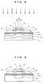
- Fig.12 and Fig.13 are sectional views showing a method for manufacturing a conventional semiconductor device of the LDD structure.
- a silicon layer 3 is provided on a silicon substrate 1 with a buried oxide film 2 which is a silicon oxide film interposed therebetween.
- Such structure including the silicon substrate 1, the oxide film 2 and the silicon layer 3 is called an SOI substrate.
- This SOI substrate is manufactured by the SIMOX method by the oxygen ion implantation method, the wafer sticking method, etc. Part of the silicon layer 3 is removed or selectively oxidized so as to be electrically isolated from other elements.
- a gate electrode 8 is provided on the silicon layer 3 with a gate insulating film 7, such as a thin oxide film of about 100 angstroms interposed therebetween.
- a channel formation region 4 for formation of a channel is provided in part of the silicon layer 3 under the gate electrode 8.
- the conductivity type of the channel formation region 4 is P-type in NMOS and it is N-type in PMOS, which is formed by introducing impurities of a conductivity type opposite to that of the source, drain portions, but which may be of the accumulation mode in which impurities of the same conductivity type as the source and drain are introduced, according to circumstances.
- the accumulation mode allows a low threshold voltage.
- Sidewalls 9 are formed on the side wall of the gate electrode 8 above the channel formation region 4.
- An additional drain region 5 and an additional source region 5' are formed under the sidewalls 9, 9, and a drain region 6 and a source region 6' are formed adjacent to the additional drain region 5 and the additional source region 5', respectively.
- the additional drain region 5 and the additional source region 5' are used to moderate the drain electric field to enhance the operational breakdown voltage.
- drain region 6, the source region 6' and the gate electrode 8 are respectively connected to metal lines with low resistance, such as aluminum, for extension to enable connections with other transistors, and the like.
- the silicon layer 3 is formed on the silicon substrate 1 with the buried oxide film 2 interposed therebetween to realize the SOI structure.
- such structure is formed by performing a high temperature heat treatment at about 1300°C after adding oxygen ions of about 0.4-2.0 ⁇ 10 18 /cm 2 into the silicon substrate 1.
- a film thickness of the buried oxide film 2 is 800 angstroms.
- the method of forming by sticking silicon substrates with oxidized surface may also be adopted.
- part of the silicon layer 3 is removed by the reactive ion etching (RIE) using photoresist and an active region for formation of elements is formed in the remaining region.
- the active region may be formed by oxidizing an isolation region by the selective oxidation method.
- boron of about 5 ⁇ 10 11 /cm 2 is implanted at 20 keV to form the channel formation region 4 in the silicon layer 3.
- a gate electrode material formed of an n-type polysilicon film doped with phosphorus is deposited.
- photoresist (not shown) is provided in a region to be the gate electrode 8 and the polysilicon film is etched using it as a mask to form the gate electrode 8.
- phosphorus is added to about 1 ⁇ 10 13 cm 2 at 30 keV to form the additional drain region 5 and the additional source region 5'.
- the sidewalls 9 are formed on the side wall of the gate electrode 8 by RIE.
- arsenic is added to about 2 ⁇ 10 15 /cm 2 at 50 keV to form the drain region 6 and the source region 6', thus obtaining the structure shown in Fig.13.
- V is an applied voltage applied over the buried oxide film 2
- q is an elementary electric charge amount
- Na is a substrate concentration
- t box is a film thickness of the buried oxide film 2
- ⁇ ox is a dielectric constant of the silicon oxide film.
- the gate material is n + polysilicon gate
- the gate voltage is 0V
- the drain voltage is 0.1V. It is well seen from the results of the device simulation that the potential rises in the silicon substrate 1.
- the substrate concentration of the silicon substrate 1 is set to 1 ⁇ 10 18 /cm 3 and the film thickness of the buried oxide film is set to 800 angstroms, the thickness of a depletion layer becomes very small as about 100 angstroms in the case of application of 2.5 V. Accordingly, the increase of the potential under the channel formation region 4 can be suppressed to suppress the short channel effect.
- a semiconductor device comprises a semiconductor substrate of a first conductivity type and having a first impurity concentration, an insulating layer formed on the semiconductor substrate, a semiconductor layer formed on the insulating layer, the semiconductor layer including a region of a second conductivity type, a gate insulating film selectively formed on the semiconductor layer, a gate electrode formed on the gate insulating film, and first and second sidewalls respectively formed on sides of the gate electrode, wherein the semiconductor layer is defined as a channel formation region under the gate insulating film, defined as first and second additional semiconductor regions of the second conductivity type under the first and second sidewalls, and defined as first and second semiconductor regions of the second conductivity type in regions adjacent respectively to the first and second additional semiconductor regions on sides opposite to the channel formation region, and a predetermined voltage is applied to the gate electrode to cause a current to flow between the first semiconductor region and the second semiconductor region through the channel formation region, and wherein the semiconductor substrate has a high concentration region of the first conductivity type and having a
- the gate electrode comprises a first partial gate electrode formed on the gate insulating film and a second partial gate electrode formed on the first partial gate electrode, and at least one of the first and second partial gate electrodes is formed of a refractory metal.
- a semiconductor device comprises a semiconductor substrate of a first conductivity type and having a first impurity concentration, an insulating layer formed on the semiconductor substrate, a semiconductor layer formed on the insulating layer, the semiconductor layer including a region of a second conductivity type, a gate insulating film selectively formed on the semiconductor layer, a gate electrode formed on the gate insulating film, and first and second sidewalls respectively formed on sides of the gate electrode, wherein the semiconductor layer is defined as a channel formation region under the gate insulating film, defined as first and second additional semiconductor regions of the second conductivity type under the first and second sidewalls, and defined as first and second semiconductor regions of the second conductivity type in regions adjacent respectively to the first and second additional semiconductor regions on sides opposite to the channel formation region, and a predetermined voltage is applied to the gate electrode to cause a current to flow between the first semiconductor region and the second semiconductor region through the channel formation region, and wherein the semiconductor substrate includes a high concentration region of the first conductivity type and having a second
- the first transistor comprises, the first semiconductor substrate, a first insulating layer formed on the first semiconductor substrate, a first semiconductor layer formed on the first insulating layer, the first semiconductor layer including a region of the second conductivity type, a first gate insulating film selectively formed on the first semiconductor layer, a first gate electrode formed on the first gate insulating film, and first and second sidewalls formed on sides of the first gate electrode, respectively, wherein the first semiconductor layer is defined as a first channel formation region under the first gate insulating film, defined as first and second additional semiconductor regions of the second conductivity type under the first and second sidewalls, and defined as first and second semiconductor regions of the second conductivity type in regions adjacent to the
- the first semiconductor substrate and the second semiconductor substrate are formed adjacent to each other, the first semiconductor substrate further includes a third high concentration region of the first conductivity type and having a fifth impurity concentration higher than the first impurity concentration in its surface, and the second semiconductor substrate further includes a fourth high concentration region of the second conductivity type and having a sixth impurity concentration higher than the second impurity concentration in its surface, and wherein the third high concentration region is provided with a first power-supply voltage, the fourth high concentration region is provided with a second power-supply voltage, and the first and second power-supply voltages are set so that a reverse bias is established between the first semiconductor substrate and the second semiconductor substrate.
- a method of manufacturing a semiconductor device comprises the steps of (a) preparing a base body including a semiconductor substrate of a first conductivity type and having a first impurity concentration, an insulating layer formed on the semiconductor substrate, and a semiconductor layer formed on the insulating layer, (b) selectively forming an insulating film on the semiconductor layer, (c) forming a conductive layer on the insulating film, (d) forming a resist on the conductive layer and patterning the resist into a predetermined form, (e) performing an etching process to the conductive layer using the resist as a mask, remaining conductive layer and insulating film being defined as a gate electrode and a gate insulating film, respectively, the semiconductor layer being defined as a channel formation region in a region under the gate electrode and defined as electrode regions in other region, (f) implanting impurities of the first conductivity type with predetermined implantation energy from above to form a high concentration region having a second impurity concentration higher than the
- the step (f) is carried out without removing the resist formed in the step (e).
- the conductive layer is formed of first and second partial conductive layers
- the step (c) comprises the steps of (c-1) forming the first partial conductive layer on the insulating film, and (c-2) forming the second partial conductive layer on the first partial conductive layer, one of the first and second partial conductive layers being a refractory metal layer.
- a method of manufacturing a semiconductor device comprises the steps of (a) preparing a base body including a semiconductor substrate of a first conductivity type and having a first impurity concentration, an insulating layer formed on the semiconductor substrate, and a semiconductor layer formed on the insulating layer, (b) forming a first resist on the semiconductor layer and patterning to provide an opening in the center of the first resist, (c) introducing impurities of the first conductivity type using the first resist as a mask to form a high concentration region having a second impurity concentration higher than the first impurity concentration in the surface of the semiconductor substrate under the opening of the resist, (d) selectively forming an insulating film on the semiconductor layer, (e) forming a conductive layer on the insulating film, (f) forming a second resist on the conductive layer and patterning the second resist into a predetermined form, (g) performing an etching process to the conductive layer using the second resist as a mask, the remaining conductive layer
- the semiconductor substrate has a high concentration region of the first conductivity type and having the second impurity concentration which is higher than the first impurity concentration and the high concentration region is formed from under the channel formation region to under each of the first and second semiconductor regions, in the surface of the semiconductor substrate under the channel formation region, and in a region at a predetermined depth from the surface of the semiconductor substrate under each of the first and second semiconductor regions.
- the high concentration region suppresses the extension of a depletion layer in the surface region of the semiconductor substrate under the channel formation region to surely prevent the short channel effect caused by an increase in potential in the interface of the channel formation region on the insulating layer side resulting from the effect of a depletion layer extending in the semiconductor substrate.
- a depletion layer can be extended to sufficiently reduce the junction capacitance in the vicinity of a region to be a drain region in the first and second semiconductor regions.
- the short channel effect is certainly avoided and the performance characteristics are not deteriorated, and the junction capacitance in the vicinity of the drain region can be sufficiently reduced so as to maintain the high-speed operation.
- the high concentration region cuts off contact between a potential rise on the first semiconductor region side and a potential rise on the second semiconductor region side, producing the effect of causing no trouble with the potential rise.
- the gate electrode is formed of first and second partial gate electrodes and at least one of the first and second partial gate electrodes is formed of a refractory metal layer, and the refractory metal layer serves as a layer for blocking impurity implantation with high blocking capability when impurities of the first conductivity type are added with predetermined energy to form the high concentration region after formation of the gate electrode.
- the high concentration region can be accurately formed from under the channel formation region to under each of the first and second semiconductor regions, in the surface of the semiconductor substrate under the channel formation region, in the region at a predetermined depth from the surface of the semiconductor substrate under each of the first and second semiconductor regions, so that a difference in level resulting from the gate electrode is reduced and the yield of metal interconnection formed on the gate electrode can be increased.
- the semiconductor substrate has a high concentration region of the first conductivity type and having the second impurity concentration which is higher than the first impurity concentration, and this high concentration region is formed in the surface of the semiconductor substrate extending from under the channel formation region to under part of each of the first and second additional semiconductor regions.
- the high concentration region suppresses the extension of a depletion layer in the surface region of the semiconductor substrate under the channel formation region to surely prevent the short channel effect caused by an increase in potential in the interface of the channel formation region on the insulating layer side resulted from the effect of a depletion layer extending in the semiconductor substrate.
- a depletion layer can be extended to sufficiently reduce the junction capacitance in the vicinity of a region to be a drain region in the first and second semiconductor regions.
- the high speed operation can be maintained by sufficiently reducing the junction capacitance in the vicinity of the drain region without causing deterioration of the performance characteristics by surely avoiding the short channel effect.
- ends of the high concentration region are located under part of the first and second additional semiconductor regions. It is preferable to avoid deterioration of the performance characteristics and maintain the high speed operation that the boundary of the high concentration region occurs under the first and second additional semiconductor regions because they are regions which are required to play an intermediate role between the channel formation region and the first and second semiconductor regions.
- the semiconductor device includes a first transistor of the second conductivity type and a second transistor of the first conductivity type, and the first semiconductor substrate in the first transistor has a first high concentration region of the first conductivity type and having the third impurity concentration which is higher than the first impurity concentration, and the first high concentration region is formed from under the first channel formation regions to under the respective first and second semiconductor regions, in the surface of the first semiconductor substrate under the first channel formation region, and in a region at a predetermined depth from the surface of the first semiconductor substrate under the first semiconductor region.
- the second semiconductor substrate in the second transistor includes a second high concentration region of the second conductivity type and having the fourth impurity concentration which is higher than the second impurity concentration, and the second high concentration region is formed from under the second channel formation region to under the respective third and fourth semiconductor regions, in the surface of the second semiconductor substrate under the second channel formation region, and in a region at a predetermined depth from the surface of the second semiconductor substrate under the third and fourth semiconductor regions.
- the first and second high concentration regions suppress the extension of depletion layers in the surface regions of the semiconductor substrates under the channel formation regions to surely prevent the short channel effect.
- depletion layers can be extended to sufficiently decrease the junction capacitance in the vicinity of regions to be drain regions in the first though fourth semiconductor regions. That is to say, in the CMOS structure, both the suppression of the short channel effect and a decrease in the junction capacitance can be obtained.
- both the suppression of the short channel effect and a decrease of the junction capacitance can be provided in the CMOS structure and a complementary semiconductor device formed of first and second transistors can be obtained which is capable of high speed operation without deterioration of performance characteristics.
- first semiconductor substrate and the second semiconductor substrate of the semiconductor device are formed adjacent each other and the first and second semiconductor substrates further include third and fourth high concentration regions in their surfaces, respectively, and the third high concentration region is supplied with the first power-supply voltage and the fourth high concentration region is supplied with the second power-supply voltage, and the first and second power-supply voltages are set so that a reverse bias is established between the first semiconductor substrate and the second semiconductor substrate.
- impurity ions of the first conductivity type are implanted with predetermined implantation energy from above to form a high concentration region having the second impurity concentration higher than the first impurity concentration in the semiconductor substrate, and the high concentration region is formed from under the channel formation region to under the electrode regions, in the surface of the semiconductor substrate under the channel formation region, and in a region at a predetermined depth from the surface of the semiconductor substrate under the electrode regions.
- the gate electrode serving as an ion implantation blocking layer allows accurate formation of the high concentration region in the surface of the semiconductor substrate from under the channel formation region.
- the high concentration region certainly suppresses the extension of a depletion layer in the surface region of the semiconductor substrate under the channel formation region to surely prevent the short channel effect.
- a depletion layer can be extended to sufficiently reduce the junction capacitance in the vicinity of a region to be a drain region in the electrode regions.
- a semiconductor device which can maintain the high speed operation by sufficiently reducing the junction capacitance in the vicinity of the drain region without deterioration of the performance characteristics by surely avoiding the short channel effect.
- the resist since the step (f) is carried out without removing the resist formed in the step (e), the resist also serves as an ion implantation blocking layer in addition to the gate electrode. Hence, even if the gate electrode has a relatively thin film thickness, the high concentration region can be accurately formed from under the channel formation region to under the electrode regions, in the surface of the semiconductor substrate under the channel region, and in a region at a predetermined depth from the surface of the semiconductor substrate under each of the electrode regions.
- the conductive layer is formed of the first and second partial conductive layers and one of the first and second partial conductive layers is a refractory metal layer, and the refractory metal layer serves as a layer for blocking impurity implantation with high blocking capability.
- a high concentration region can be accurately formed from under the channel formation region to under each of the first and second semiconductor regions, in the surface of the semiconductor substrate under the channel formation region, and in a region at a predetermined depth from the surface of the semiconductor substrate under each of the first and second semiconductor regions when performing the step (f), reducing the difference in level caused by the gate electrode and enhancing the yield of metal interconnection formed on the gate electrode.
- impurities of the first conductivity type are introduced using the first resist as a mask to form a high concentration region having the second impurity concentration higher than the first impurity concentration in the surface of the semiconductor substrate under the opening of the resist.
- the first and second sidewalls are formed on both sides of the gate electrode, the first and second sidewalls being formed so that the high concentration region is located from under the channel formation region to under part of each of the first and second sidewalls.
- the high concentration region certainly suppresses the extension of a depletion layer in the surface region of the semiconductor substrate under the channel formation region to surely prevent the short channel effect.
- a depletion layer can be extended to sufficiently reduce the junction capacitance in the vicinity of a region to be a drain region in the electrode regions.
- a semiconductor device which can maintain the high speed operation by sufficiently reducing the junction capacitance in the vicinity of the drain region without deteriorating the performance characteristics by surely avoiding the short channel effect.
- a positional error may occur between the high concentration region and the gate electrode because the gate electrode formed in the step (g) and the high concentration region 1 formed in the step (c) are formed independently of each other, the positional error will not cause the trouble of formation of the high concentration region extending to under the first and second semiconductor regions since the high concentration region is formed extending from under the channel formation region to under part of the first and second additional semiconductor regions.
- the present invention has been made to solve the problems describe earlier, and it is an object of the present invention to obtain a semiconductor device of the LDD structure which suppresses increase of leakage current and drain capacitance even if an SOI substrate with a thin buried oxide film is used and has both of the operational stability and high speed, and a manufacturing method thereof.
- Fig.1 is a sectional view showing the structure of a semiconductor device according to a first preferred embodiment of the present invention.
- Fig.2 is a sectional view showing effects of the semiconductor device of the first preferred embodiment.
- Fig.3 is a sectional view showing a method of manufacturing the semiconductor device of the first preferred embodiment.
- Fig.4 is a sectional view showing the method of manufacturing the semiconductor device of the first preferred embodiment.
- Fig.5 is a sectional view showing the method of manufacturing the semiconductor device of the first preferred embodiment.
- Fig.6 is a sectional view showing another method of manufacturing the semiconductor device of the first preferred embodiment.
- Fig.7 is a sectional view showing another method of manufacturing the semiconductor device of the first preferred embodiment.
- Fig.8 is a sectional view showing another mode of the semiconductor device of the first preferred embodiment.
- Fig.9 is a sectional view showing the structure of a semiconductor device according to a second preferred embodiment of the present invention.
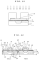
- Fig.10 is a sectional view showing a method of manufacturing the semiconductor device of the second preferred embodiment.
- Fig.11 is a sectional view showing the structure a semiconductor device according to a third preferred embodiment of the present invention.
- Fig.12 is a sectional view showing a method of manufacturing a conventional semiconductor device.
- Fig.13 is a sectional view showing the method of manufacturing the conventional semiconductor device.
- Fig.14 is a sectional view indicating a problem of the conventional semiconductor device.
- Fig.15 is a description diagram indicating the problem of the conventional semiconductor device.
- Fig.1 is a sectional view showing the structure of a semiconductor device of the LDD structure according to a first mode of a first preferred embodiment of the present invention.
- a silicon layer 3 is provided on a silicon substrate 1 with a buried oxide film 2 interposed therebetween. Part of the silicon layer 3 is removed or selectively oxidized so as to be electrically isolated from other elements.
- a gate electrode 8 is provided on the silicon layer 3 with a gate insulating film 7, such as a thin oxide film of about 100 angstroms interposed therebetween.
- a channel formation region 4 for formation of a channel is provided in part of the silicon layer 3 under the gate electrode 8.
- the conductivity type of the channel formation region 4 is P-type in NMOS and N-type in PMOS, which is formed by introducing impurities of a conductivity type opposite to that of the source, drain portions, but which may be of the accumulation mode in which impurities of the same conductivity type as the source and drain are introduced according to circumstances.
- Sidewalls 9 are formed on the side wall of the gate electrode 8 on both sides of the channel formation region 4.
- An additional drain region 5 and an additional source region 5' are formed under the sidewalls 9, 9, and a drain region 6 and a source region 6' are formed adjacent to the additional drain region 5 and the additional source region 5', respectively.
- the additional drain region 5 and the additional source region 5' are used to moderate the drain electric field to enhance the operational breakdown voltage.
- drain region 6, the source region 6' and the gate electrode 8 are respectively connected to metal lines with low resistance, such as aluminum, for extension to enable connections with other transistors, and the like.
- a high concentration region 11 with boron of about 1 ⁇ 10 18 /cm 3 introduced therein is formed extending from under the channel formation region 4 to under the drain region 6 and the source region 6' in the silicon substrate 1, as shown in Fig.1.
- This high concentration region 11 is formed in the surface of the silicon substrate 1 under the channel formation region 4, and is formed at a certain depth from the surface of the silicon substrate 1 under the drain region 6 and the source region 6'.
- Other region of the silicon substrate 1 than the high concentration region 11 is all a low concentration region with boron of about 1 ⁇ 10 15 -1 ⁇ 10 16 /cm 3 introduced therein, so that a low concentration region 10 is formed in the surface of the silicon substrate 1 under the drain region 6 and the source region 6'.
- the low concentration region 10 is formed in the surface of the silicon substrate 1 under the drain region 6 and the source region 6' and its impurity concentration is set to a low concentration of about 1 ⁇ 10 15 -1 ⁇ 10 16 /cm 3 , the depletion layer 16 deeply extends to about 1.8 ⁇ m-4500 angstroms in the vicinity of the drain when the drain voltage is 2.5 V, as shown in Fig.2, which reduces junction capacitance in this region and maintains high speed operation without incurring operational reduction.
- the buried oxide film 2 has a thickness of 800 angstroms
- formation of the low concentration region 10 of about 1 ⁇ 10 15 /cm 3 allows the depletion layer to extend by about 1.8 ⁇ m, reducing the capacitance in this region (called drain capacitance) to 1/8 as compared with the case of using a high concentration substrate. Accordingly, if a simple circuit with negligible interconnection capacitance is considered, contribution of the drain capacitance to the speed is about 50%, and the total capacitance can be reduced to about 60%, thus enhancing the speed performance by about 1.7 times.
- the high concentration region 11 is formed from the drain region 6 to the source region 6 and the high concentration region 11 cuts off contact between the potential rise on the drain side and the potential rise on the source side, no trouble occurs with the potential rise.
- Fig.3-Fig.5 are sectional views showing a manufacturing method of the first mode of the first preferred embodiment.
- the silicon layer 3 is formed on the silicon substrate 1 with the buried oxide film 2 interposed therebetween.
- oxygen ions of about 0.4-2.0 ⁇ 10 18 /cm 2 are added into the silicon substrate, and then a high temperature heat treatment at about 1300°C is performed to form such structure.
- a method of forming by sticking silicon substrates with oxidized surface may also be adopted.
- part of the silicon layer 3 is removed by the reactive ion etching (RIE) using photoresist, and an active region in which elements are formed is formed in the remaining region.
- an active region may be formed by oxidizing isolation region by the selective oxidation method.
- boron is added by about 5x10 11 /cm 2 at 20 keV to form the channel formation region 4.
- the p-type impurities are introduced, but n-type impurities may be introduced according to circumstances.
- the gate insulating film 7 of about 100 angstroms interposed therebetween, a gate electrode material formed of an n-type polysilicon film with phosphorus doped therein is deposited.
- a photoresist 14 is provided in the region to be the gate electrode 8, and the polysilicon film is etched using the photoresist 14 as a mask to form the gate electrode 8.
- an implant of boron is applied with the photoresist 14 left on the gate electrode 8, and the surface high concentration region 11 is formed in the silicon substrate 1 under the channel formation region 4 as shown in Fig.4.
- the high concentration region 11 is formed at a certain depth from the surface of the silicon substrate 1 under the region other than the channel formation region 4.
- the formation of the high concentration region 11 can be realized by implanting boron with implantation energy adjusted so that the impurity concentration in the interface of the silicon substrate 1 under the channel formation region 4 where the gate electrode 8 exists is in the order of 10 18 /cm 3 , and under the regions where the source, drain regions 6, 6' are formed, the concentration of the inside of the silicon substrate 1 is high and that in the surface remains a low concentration of the order of 10 15 -10 16 /cm 3 .
- the gate electrode 8 is formed of polysilicon, and if its film thickness is 2000 angstroms, the film thickness of the photoresist 14 is 1 ⁇ m, the film thickness of the silicon layer 4 is 500 angstroms, and the film thickness of the buried oxide film layer 2 is 800 angstroms, and when the implantation energy of boron is set to 650 keV and a dose thereof is set to 10 14 /cm 2 , the concentration in the silicon substrate 1 interface under the channel formation region 4 will be set to about 10 18 /cm 3 , the surface concentration of the silicon substrate 1 under the regions in which the source, drain regions 6, 6' are formed will be set to about 5 ⁇ 10 15 /cm 3 , and the concentration inside of the silicon substrate 1 under the regions in which the source, drain regions 6, 6' are formed will be set to the order of 10 18 /cm 3 , respectively.
- the gate electrode 8 and the photoresist 14 serve as ion implantation block layers, the high concentration region 11 can be accurately formed only in the surface of the silicon substrate 1 under the channel formation region 4.
- phosphorus is added by about 1 ⁇ 10 13 /cm 2 at 30 keV to form the n-type additional drain region 5 and the additional source region 5'.
- the sidewall 9 is formed on the side wall of the gate electrode 8 by the RIE.
- arsenic is added by about 2 ⁇ 10 15 /cm 2 at 50 keV to form the n-type drain region 6 and the source region 6', and thus the structure shown in Fig.5 is obtained.
- the first mode of the first preferred embodiment has been shown in an example of the NMOS, but it is a matter of course that the same structure can be obtained in the PMOS only with opposite conductivity.
- the structure shown in Fig.6 with the sidewall 9, the additional drain region 5, the additional source region 5', the drain region 6 and the source region 6' is obtained by using the processes described above as they are except the process of forming the high concentration region 11 and then boron 12 is implanted using the gate electrode 8 as a mask to form the high concentration region 11, as shown in Fig.7.
- the second mode it is only the gate electrode 8 that serves as a layer for blocking impurity implantation, it is therefore necessary to appropriately select the film thickness of the gate electrode 8 so that the difference in concentration is large between the high concentration region 11 under the channel formation region 4 and the low concentration region 10 under the source, drain regions 6, 6'.
- the high concentration region 11 can be formed more accurately in the region from under the channel formation region 4 to under the drain region 6 and the source region 6', in the surface of the silicon substrate 1 under the channel formation region 4 and in a region at a certain depth from the surface of the silicon substrate 1 under the drain region 6 and the source region 6', even if the film thickness of the gate electrode 8 is relatively thin, for the photoresist 14 also serves as an ion implantation blocking layer.
- Fig.8 is a sectional view showing a third mode of the first preferred embodiment.
- the gate electrode 8 is formed of a polysilicon layer 17 and a refractory metal 13, such as WSi 2 etc., as shown in Fig.8, so that the refractory metal layer 13 serves as a implantation block layer with high blocking ability to impurities such as boron forming the high concentration region, and therefore the low concentration region 10 and the high concentration region 11 can be accurately formed without making large the film thickness of the gate electrode 8.
- the gate electrode 8 of the third mode is manufactured as follows.
- a refractory metal layer is formed. Then, photoresist is provided in the region to be the gate electrode 8 and the polysilicon film and the refractory metal layer are etched using the photoresist as a mask to form the gate electrode 8 formed of the polysilicon layer 17 and the refractory metal layer 13.
- an implant of boron is applied to form the high concentration region 11 in a surface of the silicon substrate 1 under the channel formation region 4 as shown in Fig.8.
- the high concentration region 11 is formed at a predetermined depth from the surface of the silicon substrate 1 under the drain region 6 and the source region 6'.
- Other processes are the same as those in the manufacturing method of the first mode described referring to Fig.3 through Fig.5.
- Fig.9 is a sectional view showing the structure of a semiconductor device with the LDD structure of a second preferred embodiment of the present invention.
- the high concentration region 11 is formed only in the surface of the silicon substrate 1 under the channel formation region 4, and part of the additional drain region 5 and the additional source region 5'.
- the high concentration region 11 was formed inside of the silicon substrate 1 under the source, drain regions 6, 6', but it exists only under the channel formation region 4 in the second preferred embodiment, and only the impurities of about 10 15 /cm 3 initially doped in the silicon substrate 1 exist in all the region of the silicon substrate 1 under the source, drain regions 6, 6'.
- Other structure is the same as that of the first preferred embodiment shown in Fig.1, and description thereof is not repeated.
- a depletion layer deeply extends to about 1.8 ⁇ m-4500 angstroms in the vicinity of the drain when the drain voltage is 2.5V, which reduces the capacitance in this region, and high speed operation can be maintained without incurring operational reduction.
- the boundary between the high concentration region 11 and the silicon substrate 1 in the semiconductor device of the second preferred embodiment lies under part of the additional drain region 5 and the additional source region 5'.
- the additional drain region 5 and the additional source region 5' are required to play an intermediate role between the channel formation region 4 and the drain region 6 (the source region 6')
- occurrence of the boundary between the high concentration region 11 and the silicon substrate 1 under this region is preferable to prevent deterioration of the performance characteristics and to maintain high speed operation.
- An SOI substrate having a silicon layer 3 of 50 nm on a buried oxide film layer 2 of 80 nm is used as a starting material.
- photoresist 15 of about 1 ⁇ m is applied and an opening is formed in a portion where the gate electrode 8 and the channel formation region 4 are formed.
- boron of about 1 ⁇ 10 13 /cm 2 is implanted with implantation energy of 40 keV. Under this condition, the concentration in the outermost surface of the silicon substrate 1 under the channel formation region 4 becomes about 1 ⁇ 10 18 /cm 3 , and the high concentration region 11 is formed.
- the gate electrode 8, the sidewall 9, the additional drain, source regions 5, 5' and the drain, source regions 6, 6' are sequentially formed according to the same processes in the first preferred embodiment except the process of forming the high concentration region 11, and then interconnections are provided thus to obtain a desired structure.
- the occurrence of positional error will not produce a trouble that the high concentration region 11 is formed as far as under the drain region 6, or the source region 6', for the high concentration region 11 is formed extending from under the channel formation region 4 to under part of the additional drain region 5 and the additional source region 5'.
- Fig.11 is a sectional view showing a semiconductor device with the LDD structure of a third preferred embodiment.
- the third preferred embodiment shows a CMOS structure with an NMOS transistor and a PMOS transistor.
- letters N, P are added to the characters indicative of corresponding parts in the NMOS and PMOS, as 5N, 5P, etc.
- the NMOS transistor is formed on a p-type substrate region 18 and the PMOS transistor is formed on an n-type substrate region 19.
- the p-type substrate region 18 and the n-type substrate region 19 are formed adjacent each other. Further, the p-type substrate region 18 is connected to an NMOS substrate electrode 22, to which a ground potential is applied, through a p-type body region 20 formed in its surface and the n-type substrate region 19 is connected to a PMOS substrate electrode 23, to which a power-supply potential is applied, through an n-type body region 21 formed in its surface.
- a low concentration region 10N (10P) is formed in the surface of the p-type substrate region 18 (the n-type substrate region 19) under a drain region 6N (6P) and a source region 6' (6'P) and its impurity concentration is set to a low concentration of about 1 ⁇ 10 15 -1 ⁇ 10 16 /cm 3 , so that the capacitance in this region can be reduced and high speed operation can be maintained without incurring operational reduction.
Landscapes
- Engineering & Computer Science (AREA)
- Power Engineering (AREA)
- Microelectronics & Electronic Packaging (AREA)
- Physics & Mathematics (AREA)
- Condensed Matter Physics & Semiconductors (AREA)
- General Physics & Mathematics (AREA)
- Computer Hardware Design (AREA)
- Ceramic Engineering (AREA)
- Manufacturing & Machinery (AREA)
- Insulated Gate Type Field-Effect Transistor (AREA)
- Electrodes Of Semiconductors (AREA)
- Thin Film Transistor (AREA)
Abstract
Description
- The present invention relates to a semiconductor device of the LDD structure formed on an insulating substrate and a manufacturing method thereof.
- Fig.12 and Fig.13 are sectional views showing a method for manufacturing a conventional semiconductor device of the LDD structure.
- As shown in Fig.13, a
silicon layer 3 is provided on asilicon substrate 1 with a buriedoxide film 2 which is a silicon oxide film interposed therebetween. Such structure including thesilicon substrate 1, theoxide film 2 and thesilicon layer 3 is called an SOI substrate. This SOI substrate is manufactured by the SIMOX method by the oxygen ion implantation method, the wafer sticking method, etc. Part of thesilicon layer 3 is removed or selectively oxidized so as to be electrically isolated from other elements. - A
gate electrode 8 is provided on thesilicon layer 3 with agate insulating film 7, such as a thin oxide film of about 100 angstroms interposed therebetween. Achannel formation region 4 for formation of a channel is provided in part of thesilicon layer 3 under thegate electrode 8. Usually, the conductivity type of thechannel formation region 4 is P-type in NMOS and it is N-type in PMOS, which is formed by introducing impurities of a conductivity type opposite to that of the source, drain portions, but which may be of the accumulation mode in which impurities of the same conductivity type as the source and drain are introduced, according to circumstances. The accumulation mode allows a low threshold voltage. -
Sidewalls 9 are formed on the side wall of thegate electrode 8 above thechannel formation region 4. Anadditional drain region 5 and an additional source region 5' are formed under thesidewalls drain region 6 and a source region 6' are formed adjacent to theadditional drain region 5 and the additional source region 5', respectively. - In such a structure, if a certain gate voltage is applied to the
gate electrode 8, carriers of the same conductivity type as the source, drain are caused in thechannel formation region 4, and the amount the carriers changes depending on the applied gate voltage, and thus the MOS operation of controlling the current value with the gate voltage is obtained. - The
additional drain region 5 and the additional source region 5' are used to moderate the drain electric field to enhance the operational breakdown voltage. - Actually, the
drain region 6, the source region 6' and thegate electrode 8 are respectively connected to metal lines with low resistance, such as aluminum, for extension to enable connections with other transistors, and the like. - Next, a method of manufacturing this structure will be described.
- As shown in Fig.12, the
silicon layer 3 is formed on thesilicon substrate 1 with the buriedoxide film 2 interposed therebetween to realize the SOI structure. Usually, such structure is formed by performing a high temperature heat treatment at about 1300°C after adding oxygen ions of about 0.4-2.0×10¹⁸/cm2 into thesilicon substrate 1. In the case of a dose of 0.4×10¹⁸/cm2, a film thickness of the buriedoxide film 2 is 800 angstroms. The method of forming by sticking silicon substrates with oxidized surface may also be adopted. - Next, part of the
silicon layer 3 is removed by the reactive ion etching (RIE) using photoresist and an active region for formation of elements is formed in the remaining region. The active region may be formed by oxidizing an isolation region by the selective oxidation method. Next, boron of about 5×10¹¹/cm2 is implanted at 20 keV to form thechannel formation region 4 in thesilicon layer 3. Although impurities of p-type are introduced herein, impurities of n-type may possibly be introduced depending on circumstances. - Subsequently, with the
gate insulating film 7 of about 100 angstroms interposed therebetween, a gate electrode material formed of an n-type polysilicon film doped with phosphorus is deposited. Now, photoresist (not shown) is provided in a region to be thegate electrode 8 and the polysilicon film is etched using it as a mask to form thegate electrode 8. After removing the photoresist, phosphorus is added to about 1×1013cm2 at 30 keV to form theadditional drain region 5 and the additional source region 5'. Furthermore, after depositing a CVD oxide film of about 1500 angstroms, thesidewalls 9 are formed on the side wall of thegate electrode 8 by RIE. Next, arsenic is added to about 2×10¹⁵/cm2 at 50 keV to form thedrain region 6 and the source region 6', thus obtaining the structure shown in Fig.13. - If a low dose substrate with the buried
oxide film 2 thinner than about 1000 angstroms is used as an SOI substrate, there were problems as described below. First, if the concentration of thesilicon substrate 1 is low, a depletion layer deeply extends in the silicon substrate. The length td of the depletion layer is obtained from the equation (I) below.
- Here, V is an applied voltage applied over the buried
oxide film 2, q is an elementary electric charge amount, Na is a substrate concentration, t box is a film thickness of the buriedoxide film 2 and ε ox is a dielectric constant of the silicon oxide film. - In the case of the substrate concentration (concentration of impurity of the substrate) of 1×10¹⁵/cm3 and the film thickness of the buried
oxide film 2 of 800 angstroms, when the applied voltage V is 2.5 V, a width of the depletion layer in the vicinity of the drain reaches 1.8 µm. If the depletion layer extends such long, as shown by the arrow in Fig.14, potential in thesilicon substrate 1 under thechannel formation region 4 increases. The increase of the potential in thesilicon substrate 1 increases potential in the lower part of thechannel formation region 4 itself, causing a problem of being weak to the short channel effect. - Fig.15 shows the potential distribution of an NMOS with the single drain structure with the channel length (gate length) L=0.5 µm, a film thickness of the
silicon layer 3 of 1000 angstroms, a film thickness of the buriedoxide film 2 of 800 angstroms, an impurity concentration of thesilicon substrate 1 of 1×10¹⁴/cm3 and an impurity concentration of thechannel formation region 4 of 5×10¹⁶/cm3, which was obtained by device simulation. Here, the gate material is n+ polysilicon gate, the gate voltage is 0V, and the drain voltage is 0.1V. It is well seen from the results of the device simulation that the potential rises in thesilicon substrate 1. - In order to suppress the increase of the potential, a method of increasing the substrate concentration of the
silicon substrate 1 is possible. For example, if the substrate concentration is set to 1×10¹⁸/cm3 and the film thickness of the buried oxide film is set to 800 angstroms, the thickness of a depletion layer becomes very small as about 100 angstroms in the case of application of 2.5 V. Accordingly, the increase of the potential under thechannel formation region 4 can be suppressed to suppress the short channel effect. - As a result of increasing the substrate concentration of the
silicon substrate 1, however, the extension of a depletion layer in thesilicon substrate 1 under thedrain region 6 is also suppressed, increasing the junction capacitance in this region, and which will produce another problem that the high speed operation, which is a feature of the SOI, is not obtained. - The problems of the conventional semiconductor device of the LDD structure discussed above can be summarized as follows.
- * If the concentration of the silicon substrate is low, a depletion layer extends under the channel formation region and potential in that region increases. This will cause an increase in potential in the lower portion of the channel formation region (in the interface with the buried oxide film), increase the leakage current, and deteriorate performance characteristics.
- * Increasing the concentration of the silicon substrate to suppress the potential increase to suppress the leakage current will also suppress the extension of a depletion layer under the drain to increase the drain capacitance, and which will reduce the operation speed.
- According to a first aspect of the present invention, a semiconductor device comprises a semiconductor substrate of a first conductivity type and having a first impurity concentration, an insulating layer formed on the semiconductor substrate, a semiconductor layer formed on the insulating layer, the semiconductor layer including a region of a second conductivity type, a gate insulating film selectively formed on the semiconductor layer, a gate electrode formed on the gate insulating film, and first and second sidewalls respectively formed on sides of the gate electrode, wherein the semiconductor layer is defined as a channel formation region under the gate insulating film, defined as first and second additional semiconductor regions of the second conductivity type under the first and second sidewalls, and defined as first and second semiconductor regions of the second conductivity type in regions adjacent respectively to the first and second additional semiconductor regions on sides opposite to the channel formation region, and a predetermined voltage is applied to the gate electrode to cause a current to flow between the first semiconductor region and the second semiconductor region through the channel formation region, and wherein the semiconductor substrate has a high concentration region of the first conductivity type and having a second impurity concentration higher than the first impurity concentration, the high concentration region being formed extending from under the channel formation region to under the respective first and second semiconductor regions, the high concentration region being formed in a surface of the semiconductor substrate under the channel formation region, and in a region at a predetermined depth from the surface of the semiconductor substrate under the respective first and second semiconductor regions.
- Preferably, according to a semiconductor device of a second aspect of the present invention, the gate electrode comprises a first partial gate electrode formed on the gate insulating film and a second partial gate electrode formed on the first partial gate electrode, and at least one of the first and second partial gate electrodes is formed of a refractory metal.
- In a third aspect of the present invention, a semiconductor device comprises a semiconductor substrate of a first conductivity type and having a first impurity concentration, an insulating layer formed on the semiconductor substrate, a semiconductor layer formed on the insulating layer, the semiconductor layer including a region of a second conductivity type, a gate insulating film selectively formed on the semiconductor layer, a gate electrode formed on the gate insulating film, and first and second sidewalls respectively formed on sides of the gate electrode, wherein the semiconductor layer is defined as a channel formation region under the gate insulating film, defined as first and second additional semiconductor regions of the second conductivity type under the first and second sidewalls, and defined as first and second semiconductor regions of the second conductivity type in regions adjacent respectively to the first and second additional semiconductor regions on sides opposite to the channel formation region, and a predetermined voltage is applied to the gate electrode to cause a current to flow between the first semiconductor region and the second semiconductor region through the channel formation region, and wherein the semiconductor substrate includes a high concentration region of the first conductivity type and having a second impurity concentration higher than the first impurity concentration, the high concentration region being formed in a surface of the semiconductor substrate extending from under the channel formation region to under parts of the respective first and second additional semiconductor regions.
- According to a fourth aspect of the present invention, in a semiconductor device comprising a first transistor of a second conductivity type formed on a first semiconductor substrate of a first conductivity type and having a first impurity concentration and a second transistor of the first conductivity type formed on a second semiconductor substrate of the second conductivity type and having a second impurity concentration, the first transistor comprises, the first semiconductor substrate, a first insulating layer formed on the first semiconductor substrate, a first semiconductor layer formed on the first insulating layer, the first semiconductor layer including a region of the second conductivity type, a first gate insulating film selectively formed on the first semiconductor layer, a first gate electrode formed on the first gate insulating film, and first and second sidewalls formed on sides of the first gate electrode, respectively, wherein the first semiconductor layer is defined as a first channel formation region under the first gate insulating film, defined as first and second additional semiconductor regions of the second conductivity type under the first and second sidewalls, and defined as first and second semiconductor regions of the second conductivity type in regions adjacent to the first and second additional semiconductor regions respectively on sides opposite to the first channel formation region, and a predetermined voltage is applied to the first gate electrode to cause a current to flow between the first semiconductor region and the second semiconductor region through the channel formation region, and wherein the first semiconductor substrate includes a first high concentration region of the first conductivity type and having a third impurity concentration higher than the first impurity concentration, the first high concentration region being formed extending from under the first channel formation region to under the respective first and second semiconductor regions, the first high concentration region being formed in a surface of the first semiconductor substrate under the first channel formation region, and in a region at a predetermined depth from the surface of the first semiconductor substrate under the respective first and second semiconductor regions, and the second transistor comprises, the second semiconductor substrate, a second insulating layer formed on the second semiconductor substrate, a second semiconductor layer formed on the second insulating layer, the second semiconductor layer including a region of the first conductivity type, a second gate insulating film selectively formed on the second semiconductor layer, a second gate electrode formed on the second gate insulating film, and third and fourth sidewalls formed on sides of the second gate electrode, respectively, wherein the second semiconductor layer is defined as a second channel formation region under the second gate insulating film, defined as third and fourth additional semiconductor regions of the first conductivity type under the third and fourth sidewalls, and defined as third and fourth semiconductor regions of the first conductivity type in regions adjacent to the third and fourth additional semiconductor regions, respectively, on sides opposite to the second channel formation region, and a predetermined voltage is applied to the second gate electrode to cause a current to flow between the third semiconductor region and the fourth semiconductor region through the second channel formation region, and wherein the second semiconductor substrate includes a second high concentration region of the second conductivity type and having a fourth impurity concentration higher than the second impurity concentration, the second high concentration region being formed extending from under the second channel formation region to under the respective third and fourth semiconductor regions, the second high concentration region being formed in a surface of the second semiconductor substrate under the second channel formation region, and in a region at a predetermined depth from the surface of the second semiconductor substrate under the respective third and fourth semiconductor regions.
- Preferably, according to a semiconductor device of a fifth aspect of the present invention, the first semiconductor substrate and the second semiconductor substrate are formed adjacent to each other, the first semiconductor substrate further includes a third high concentration region of the first conductivity type and having a fifth impurity concentration higher than the first impurity concentration in its surface, and the second semiconductor substrate further includes a fourth high concentration region of the second conductivity type and having a sixth impurity concentration higher than the second impurity concentration in its surface, and wherein the third high concentration region is provided with a first power-supply voltage, the fourth high concentration region is provided with a second power-supply voltage, and the first and second power-supply voltages are set so that a reverse bias is established between the first semiconductor substrate and the second semiconductor substrate.
- According to a sixth aspect of the present invention, a method of manufacturing a semiconductor device comprises the steps of (a) preparing a base body including a semiconductor substrate of a first conductivity type and having a first impurity concentration, an insulating layer formed on the semiconductor substrate, and a semiconductor layer formed on the insulating layer, (b) selectively forming an insulating film on the semiconductor layer, (c) forming a conductive layer on the insulating film, (d) forming a resist on the conductive layer and patterning the resist into a predetermined form, (e) performing an etching process to the conductive layer using the resist as a mask, remaining conductive layer and insulating film being defined as a gate electrode and a gate insulating film, respectively, the semiconductor layer being defined as a channel formation region in a region under the gate electrode and defined as electrode regions in other region, (f) implanting impurities of the first conductivity type with predetermined implantation energy from above to form a high concentration region having a second impurity concentration higher than the first impurity concentration in the semiconductor substrate, the high concentration region being formed extending from under the channel formation region to under the electrode regions, the high concentration region being formed in a surface of the semiconductor substrate under the channel formation region, and in a region at a predetermined depth from the surface of the semiconductor substrate under the electrode regions, (g) introducing impurities of the second conductivity type into the semiconductor layer using the gate electrode as a mask, (h) forming first and second sidewalls on both sides of the gate electrode, and (i) introducing impurities of the second conductivity type into the semiconductor layer using the gate electrode and the first and second sidewalls as masks, the semiconductor layer being defined as first and second additional semiconductor regions of the second conductivity type under the first and second sidewalls, and defined as first and second semiconductor regions of the second conductivity type in regions respectively adjacent to the first and second additional semiconductor regions on sides opposite to the channel formation region, a predetermined voltage is applied to the gate electrode to cause a current to flow between the first semiconductor region and the second semiconductor region through the channel formation region.
- Preferably, according to a method of manufacturing a semiconductor device of a seventh aspect of the present invention, the step (f) is carried out without removing the resist formed in the step (e).
- Preferably, according to a method of manufacturing a semiconductor device of an eighth aspect of the present invention, the conductive layer is formed of first and second partial conductive layers, and the step (c) comprises the steps of (c-1) forming the first partial conductive layer on the insulating film, and (c-2) forming the second partial conductive layer on the first partial conductive layer, one of the first and second partial conductive layers being a refractory metal layer.
- According to a ninth aspect of the present invention, a method of manufacturing a semiconductor device comprises the steps of (a) preparing a base body including a semiconductor substrate of a first conductivity type and having a first impurity concentration, an insulating layer formed on the semiconductor substrate, and a semiconductor layer formed on the insulating layer, (b) forming a first resist on the semiconductor layer and patterning to provide an opening in the center of the first resist, (c) introducing impurities of the first conductivity type using the first resist as a mask to form a high concentration region having a second impurity concentration higher than the first impurity concentration in the surface of the semiconductor substrate under the opening of the resist, (d) selectively forming an insulating film on the semiconductor layer, (e) forming a conductive layer on the insulating film, (f) forming a second resist on the conductive layer and patterning the second resist into a predetermined form, (g) performing an etching process to the conductive layer using the second resist as a mask, the remaining conductive layer and insulating film being defined as a gate electrode and a gate insulating film, respectively, the semiconductor layer being defined as a channel formation region in a region under the gate electrode and defined as electrode regions in other region, (h) adding impurities of the second conductivity type into the semiconductor layer using the gate electrode as a mask, (i) forming first and second sidewalls on both sides of the gate electrode, the first and second sidewalls being formed so that the high concentration region is located from under the channel formation region to under parts of the respective first and second sidewalls, and (j) introducing impurities of the second conductivity type into the semiconductor layer using the gate electrode and the first and second sidewalls as masks, the semiconductor layer being defined as first and second additional semiconductor regions of the second conductivity type under the first and second sidewalls, and defined as first and second semiconductor regions of the second conductivity type in regions adjacent to the first and second additional semiconductor regions, respectively, on sides opposite to the channel formation region, and a predetermined voltage is applied to the gate electrode to cause a current to flow between the first semiconductor region and the second semiconductor region through the channel formation region.
- According to the first aspect of the present invention, the semiconductor substrate has a high concentration region of the first conductivity type and having the second impurity concentration which is higher than the first impurity concentration and the high concentration region is formed from under the channel formation region to under each of the first and second semiconductor regions, in the surface of the semiconductor substrate under the channel formation region, and in a region at a predetermined depth from the surface of the semiconductor substrate under each of the first and second semiconductor regions.
- Accordingly, when a predetermined voltage is applied to the gate electrode to enter an operation state, the high concentration region suppresses the extension of a depletion layer in the surface region of the semiconductor substrate under the channel formation region to surely prevent the short channel effect caused by an increase in potential in the interface of the channel formation region on the insulating layer side resulting from the effect of a depletion layer extending in the semiconductor substrate.
- Furthermore, as the surface region of the semiconductor substrate under the first and second semiconductor regions is set to the first impurity concentration which is relatively low, a depletion layer can be extended to sufficiently reduce the junction capacitance in the vicinity of a region to be a drain region in the first and second semiconductor regions.
- As a result, the short channel effect is certainly avoided and the performance characteristics are not deteriorated, and the junction capacitance in the vicinity of the drain region can be sufficiently reduced so as to maintain the high-speed operation.
- In addition, as the high concentration region is formed extending from under the channel formation region to the first and second semiconductor regions, the high concentration region cuts off contact between a potential rise on the first semiconductor region side and a potential rise on the second semiconductor region side, producing the effect of causing no trouble with the potential rise.
- According to the second aspect of the present invention, the gate electrode is formed of first and second partial gate electrodes and at least one of the first and second partial gate electrodes is formed of a refractory metal layer, and the refractory metal layer serves as a layer for blocking impurity implantation with high blocking capability when impurities of the first conductivity type are added with predetermined energy to form the high concentration region after formation of the gate electrode.
- As a result, even if the film thickness of the gate electrode is relatively small, the high concentration region can be accurately formed from under the channel formation region to under each of the first and second semiconductor regions, in the surface of the semiconductor substrate under the channel formation region, in the region at a predetermined depth from the surface of the semiconductor substrate under each of the first and second semiconductor regions, so that a difference in level resulting from the gate electrode is reduced and the yield of metal interconnection formed on the gate electrode can be increased.
- According to the third aspect of the present invention, the semiconductor substrate has a high concentration region of the first conductivity type and having the second impurity concentration which is higher than the first impurity concentration, and this high concentration region is formed in the surface of the semiconductor substrate extending from under the channel formation region to under part of each of the first and second additional semiconductor regions.
- Accordingly, when a predetermined voltage is applied to the gate electrode to enter an operation state, the high concentration region suppresses the extension of a depletion layer in the surface region of the semiconductor substrate under the channel formation region to surely prevent the short channel effect caused by an increase in potential in the interface of the channel formation region on the insulating layer side resulted from the effect of a depletion layer extending in the semiconductor substrate.
- Furthermore, as the surface region of the semiconductor substrate under the first and second semiconductor regions is set to the first impurity concentration which is relatively low, a depletion layer can be extended to sufficiently reduce the junction capacitance in the vicinity of a region to be a drain region in the first and second semiconductor regions.
- As a result, the high speed operation can be maintained by sufficiently reducing the junction capacitance in the vicinity of the drain region without causing deterioration of the performance characteristics by surely avoiding the short channel effect.
- In addition, ends of the high concentration region are located under part of the first and second additional semiconductor regions. It is preferable to avoid deterioration of the performance characteristics and maintain the high speed operation that the boundary of the high concentration region occurs under the first and second additional semiconductor regions because they are regions which are required to play an intermediate role between the channel formation region and the first and second semiconductor regions.
- According to the fourth aspect of the present invention, the semiconductor device includes a first transistor of the second conductivity type and a second transistor of the first conductivity type, and the first semiconductor substrate in the first transistor has a first high concentration region of the first conductivity type and having the third impurity concentration which is higher than the first impurity concentration, and the first high concentration region is formed from under the first channel formation regions to under the respective first and second semiconductor regions, in the surface of the first semiconductor substrate under the first channel formation region, and in a region at a predetermined depth from the surface of the first semiconductor substrate under the first semiconductor region.
- The second semiconductor substrate in the second transistor includes a second high concentration region of the second conductivity type and having the fourth impurity concentration which is higher than the second impurity concentration, and the second high concentration region is formed from under the second channel formation region to under the respective third and fourth semiconductor regions, in the surface of the second semiconductor substrate under the second channel formation region, and in a region at a predetermined depth from the surface of the second semiconductor substrate under the third and fourth semiconductor regions.
- Accordingly, in the first and second transistors of the semiconductor device according to the fourth aspect, when a predetermined voltage is applied to the first and second gate electrodes to enter an operation state, the first and second high concentration regions suppress the extension of depletion layers in the surface regions of the semiconductor substrates under the channel formation regions to surely prevent the short channel effect.
- Also, as the surface regions of the semiconductor substrates under the first and second, and third and fourth semiconductor regions are set to the first and second impurity concentrations which are relatively low, depletion layers can be extended to sufficiently decrease the junction capacitance in the vicinity of regions to be drain regions in the first though fourth semiconductor regions. That is to say, in the CMOS structure, both the suppression of the short channel effect and a decrease in the junction capacitance can be obtained.
- As a result, both the suppression of the short channel effect and a decrease of the junction capacitance can be provided in the CMOS structure and a complementary semiconductor device formed of first and second transistors can be obtained which is capable of high speed operation without deterioration of performance characteristics.
- Also, the first semiconductor substrate and the second semiconductor substrate of the semiconductor device according to the fifth aspect are formed adjacent each other and the first and second semiconductor substrates further include third and fourth high concentration regions in their surfaces, respectively, and the third high concentration region is supplied with the first power-supply voltage and the fourth high concentration region is supplied with the second power-supply voltage, and the first and second power-supply voltages are set so that a reverse bias is established between the first semiconductor substrate and the second semiconductor substrate.
- Accordingly, even though the first semiconductor substrate and the second semiconductor substrate are adjacent to each other, current will not flow between the first semiconductor substrate and the second semiconductor substrate.
- According to the sixth aspect of the present invention, in the step (f) of the method of manufacturing a semiconductor device, impurity ions of the first conductivity type are implanted with predetermined implantation energy from above to form a high concentration region having the second impurity concentration higher than the first impurity concentration in the semiconductor substrate, and the high concentration region is formed from under the channel formation region to under the electrode regions, in the surface of the semiconductor substrate under the channel formation region, and in a region at a predetermined depth from the surface of the semiconductor substrate under the electrode regions.
- Then, the gate electrode serving as an ion implantation blocking layer allows accurate formation of the high concentration region in the surface of the semiconductor substrate from under the channel formation region.
- Accordingly, in the semiconductor device manufactured by the method of the sixth aspect, when a predetermined voltage is applied to the gate electrode to enter an operation state, the high concentration region certainly suppresses the extension of a depletion layer in the surface region of the semiconductor substrate under the channel formation region to surely prevent the short channel effect.
- Furthermore, as the surface region of the semiconductor substrate under the electrode regions is set to the first impurity concentration which is relatively low, a depletion layer can be extended to sufficiently reduce the junction capacitance in the vicinity of a region to be a drain region in the electrode regions.
- As a result, a semiconductor device can be obtained which can maintain the high speed operation by sufficiently reducing the junction capacitance in the vicinity of the drain region without deterioration of the performance characteristics by surely avoiding the short channel effect.
- According to the manufacturing method of a semiconductor device according to the seventh aspect of the present invention, since the step (f) is carried out without removing the resist formed in the step (e), the resist also serves as an ion implantation blocking layer in addition to the gate electrode. Hence, even if the gate electrode has a relatively thin film thickness, the high concentration region can be accurately formed from under the channel formation region to under the electrode regions, in the surface of the semiconductor substrate under the channel region, and in a region at a predetermined depth from the surface of the semiconductor substrate under each of the electrode regions.
- As a result, a difference in level caused by the gate electrode can be reduced, which provides a semiconductor device with enhanced yield of the metal interconnection formed on the gate electrode.
- According to the method of manufacturing the semiconductor device according to the eighth aspect of the present invention, the conductive layer is formed of the first and second partial conductive layers and one of the first and second partial conductive layers is a refractory metal layer, and the refractory metal layer serves as a layer for blocking impurity implantation with high blocking capability.
- As a result, even if the gate electrode has a relatively small film thickness, a high concentration region can be accurately formed from under the channel formation region to under each of the first and second semiconductor regions, in the surface of the semiconductor substrate under the channel formation region, and in a region at a predetermined depth from the surface of the semiconductor substrate under each of the first and second semiconductor regions when performing the step (f), reducing the difference in level caused by the gate electrode and enhancing the yield of metal interconnection formed on the gate electrode.
- According to the method of manufacturing a semiconductor device according to the ninth aspect of the present invention, in the step (c), impurities of the first conductivity type are introduced using the first resist as a mask to form a high concentration region having the second impurity concentration higher than the first impurity concentration in the surface of the semiconductor substrate under the opening of the resist.
- Then, in the step (i), the first and second sidewalls are formed on both sides of the gate electrode, the first and second sidewalls being formed so that the high concentration region is located from under the channel formation region to under part of each of the first and second sidewalls.
- Thus, according to the semiconductor device manufactured by the manufacturing method of the ninth aspect, when a predetermined voltage is applied to the gate electrode to enter an operation state, the high concentration region certainly suppresses the extension of a depletion layer in the surface region of the semiconductor substrate under the channel formation region to surely prevent the short channel effect.
- Furthermore, as the surface region of the semiconductor substrate under the electrode regions is set to the first impurity concentration which is relatively low, a depletion layer can be extended to sufficiently reduce the junction capacitance in the vicinity of a region to be a drain region in the electrode regions.
- As a result, a semiconductor device can be obtained which can maintain the high speed operation by sufficiently reducing the junction capacitance in the vicinity of the drain region without deteriorating the performance characteristics by surely avoiding the short channel effect.
- Further, although a positional error may occur between the high concentration region and the gate electrode because the gate electrode formed in the step (g) and the
high concentration region 1 formed in the step (c) are formed independently of each other, the positional error will not cause the trouble of formation of the high concentration region extending to under the first and second semiconductor regions since the high concentration region is formed extending from under the channel formation region to under part of the first and second additional semiconductor regions. - The present invention has been made to solve the problems describe earlier, and it is an object of the present invention to obtain a semiconductor device of the LDD structure which suppresses increase of leakage current and drain capacitance even if an SOI substrate with a thin buried oxide film is used and has both of the operational stability and high speed, and a manufacturing method thereof.
- These and other objects, features, aspects and advantages of the present invention will become more apparent from the following detailed description of the present invention when taken in conjunction with the accompanying drawing.
- Fig.1 is a sectional view showing the structure of a semiconductor device according to a first preferred embodiment of the present invention.
- Fig.2 is a sectional view showing effects of the semiconductor device of the first preferred embodiment.
- Fig.3 is a sectional view showing a method of manufacturing the semiconductor device of the first preferred embodiment.
- Fig.4 is a sectional view showing the method of manufacturing the semiconductor device of the first preferred embodiment.
- Fig.5 is a sectional view showing the method of manufacturing the semiconductor device of the first preferred embodiment.
- Fig.6 is a sectional view showing another method of manufacturing the semiconductor device of the first preferred embodiment.
- Fig.7 is a sectional view showing another method of manufacturing the semiconductor device of the first preferred embodiment.
- Fig.8 is a sectional view showing another mode of the semiconductor device of the first preferred embodiment.
- Fig.9 is a sectional view showing the structure of a semiconductor device according to a second preferred embodiment of the present invention.
- Fig.10 is a sectional view showing a method of manufacturing the semiconductor device of the second preferred embodiment.
- Fig.11 is a sectional view showing the structure a semiconductor device according to a third preferred embodiment of the present invention.
- Fig.12 is a sectional view showing a method of manufacturing a conventional semiconductor device.
- Fig.13 is a sectional view showing the method of manufacturing the conventional semiconductor device.
- Fig.14 is a sectional view indicating a problem of the conventional semiconductor device.
- Fig.15 is a description diagram indicating the problem of the conventional semiconductor device.
- Fig.1 is a sectional view showing the structure of a semiconductor device of the LDD structure according to a first mode of a first preferred embodiment of the present invention.
- As shown in the figure, a
silicon layer 3 is provided on asilicon substrate 1 with a buriedoxide film 2 interposed therebetween. Part of thesilicon layer 3 is removed or selectively oxidized so as to be electrically isolated from other elements. - A
gate electrode 8 is provided on thesilicon layer 3 with agate insulating film 7, such as a thin oxide film of about 100 angstroms interposed therebetween. Achannel formation region 4 for formation of a channel is provided in part of thesilicon layer 3 under thegate electrode 8. Usually, the conductivity type of thechannel formation region 4 is P-type in NMOS and N-type in PMOS, which is formed by introducing impurities of a conductivity type opposite to that of the source, drain portions, but which may be of the accumulation mode in which impurities of the same conductivity type as the source and drain are introduced according to circumstances. -
Sidewalls 9 are formed on the side wall of thegate electrode 8 on both sides of thechannel formation region 4. - An
additional drain region 5 and an additional source region 5' are formed under thesidewalls drain region 6 and a source region 6' are formed adjacent to theadditional drain region 5 and the additional source region 5', respectively. - In such a structure, if a certain gate voltage is applied to the
gate electrode 8, carriers of the same conductivity type as the source, drain are caused in thechannel formation region 4, and the amount of the carriers changes depending on the gate voltage, and thus the MOS operation of controlling the current value with the gate voltage is obtained. - The
additional drain region 5 and the additional source region 5' are used to moderate the drain electric field to enhance the operational breakdown voltage. - Actually, the
drain region 6, the source region 6' and thegate electrode 8 are respectively connected to metal lines with low resistance, such as aluminum, for extension to enable connections with other transistors, and the like. - In the semiconductor device of the first mode of the first preferred embodiment, a
high concentration region 11 with boron of about 1×10¹⁸/cm3 introduced therein is formed extending from under thechannel formation region 4 to under thedrain region 6 and the source region 6' in thesilicon substrate 1, as shown in Fig.1. Thishigh concentration region 11 is formed in the surface of thesilicon substrate 1 under thechannel formation region 4, and is formed at a certain depth from the surface of thesilicon substrate 1 under thedrain region 6 and the source region 6'. Other region of thesilicon substrate 1 than thehigh concentration region 11 is all a low concentration region with boron of about 1×10¹⁵-1×10¹⁶/cm3 introduced therein, so that alow concentration region 10 is formed in the surface of thesilicon substrate 1 under thedrain region 6 and the source region 6'. - This way, since formation of the
high concentration region 11 in the surface of thesilicon substrate 1 under thechannel formation region 4 sets the substrate concentration of thesilicon substrate 1 high, extension of adepletion layer 16 in this region is suppressed as shown in Fig.2 and the short channel effect caused by a rise of potential in the interface of thechannel formation region 4 on the buriedoxide film 2 side caused by the depletion layer extending in thesilicon substrate 1 can be surely prevented, as in the conventional structure, and then the leakage current is not increased and the performance characteristics are not deteriorated. - Further, since the
low concentration region 10 is formed in the surface of thesilicon substrate 1 under thedrain region 6 and the source region 6' and its impurity concentration is set to a low concentration of about 1×10¹⁵-1×10¹⁶/cm3, thedepletion layer 16 deeply extends to about 1.8 µm-4500 angstroms in the vicinity of the drain when the drain voltage is 2.5 V, as shown in Fig.2, which reduces junction capacitance in this region and maintains high speed operation without incurring operational reduction. - For example, if the buried
oxide film 2 has a thickness of 800 angstroms, formation of thelow concentration region 10 of about 1×10¹⁵/cm3 allows the depletion layer to extend by about 1.8µm, reducing the capacitance in this region (called drain capacitance) to 1/8 as compared with the case of using a high concentration substrate. Accordingly, if a simple circuit with negligible interconnection capacitance is considered, contribution of the drain capacitance to the speed is about 50%, and the total capacitance can be reduced to about 60%, thus enhancing the speed performance by about 1.7 times. - As the
high concentration region 11 is formed from thedrain region 6 to thesource region 6 and thehigh concentration region 11 cuts off contact between the potential rise on the drain side and the potential rise on the source side, no trouble occurs with the potential rise. - Fig.3-Fig.5 are sectional views showing a manufacturing method of the first mode of the first preferred embodiment.
- As shown in Fig.3, the
silicon layer 3 is formed on thesilicon substrate 1 with the buriedoxide film 2 interposed therebetween. Usually, oxygen ions of about 0.4-2.0×10¹⁸/cm2 are added into the silicon substrate, and then a high temperature heat treatment at about 1300°C is performed to form such structure. A method of forming by sticking silicon substrates with oxidized surface may also be adopted. - Next, part of the
silicon layer 3 is removed by the reactive ion etching (RIE) using photoresist, and an active region in which elements are formed is formed in the remaining region. Here, an active region may be formed by oxidizing isolation region by the selective oxidation method. Next, boron is added by about 5x10¹¹/cm2 at 20 keV to form thechannel formation region 4. Now, the p-type impurities are introduced, but n-type impurities may be introduced according to circumstances. Subsequently, with thegate insulating film 7 of about 100 angstroms interposed therebetween, a gate electrode material formed of an n-type polysilicon film with phosphorus doped therein is deposited. Here, aphotoresist 14 is provided in the region to be thegate electrode 8, and the polysilicon film is etched using thephotoresist 14 as a mask to form thegate electrode 8. - Next, an implant of boron is applied with the
photoresist 14 left on thegate electrode 8, and the surfacehigh concentration region 11 is formed in thesilicon substrate 1 under thechannel formation region 4 as shown in Fig.4. Thehigh concentration region 11 is formed at a certain depth from the surface of thesilicon substrate 1 under the region other than thechannel formation region 4. - The formation of the
high concentration region 11 can be realized by implanting boron with implantation energy adjusted so that the impurity concentration in the interface of thesilicon substrate 1 under thechannel formation region 4 where thegate electrode 8 exists is in the order of 1018/cm3, and under the regions where the source,drain regions 6, 6' are formed, the concentration of the inside of thesilicon substrate 1 is high and that in the surface remains a low concentration of the order of 1015-1016/cm3. - For example, if the
gate electrode 8 is formed of polysilicon, and if its film thickness is 2000 angstroms, the film thickness of thephotoresist 14 is 1µm, the film thickness of thesilicon layer 4 is 500 angstroms, and the film thickness of the buriedoxide film layer 2 is 800 angstroms, and when the implantation energy of boron is set to 650 keV and a dose thereof is set to 1014/cm2, the concentration in thesilicon substrate 1 interface under thechannel formation region 4 will be set to about 1018/cm3, the surface concentration of thesilicon substrate 1 under the regions in which the source,drain regions 6, 6' are formed will be set to about 5×10¹⁵/cm3, and the concentration inside of thesilicon substrate 1 under the regions in which the source,drain regions 6, 6' are formed will be set to the order of 1018/cm3, respectively. - At this time, as the
gate electrode 8 and thephotoresist 14 serve as ion implantation block layers, thehigh concentration region 11 can be accurately formed only in the surface of thesilicon substrate 1 under thechannel formation region 4. - Subsequently, after removing the
photoresist 14, phosphorus is added by about 1×10¹³/cm2 at 30 keV to form the n-typeadditional drain region 5 and the additional source region 5'. Furthermore, after depositing a CVD oxide film of about 1500 angstroms, thesidewall 9 is formed on the side wall of thegate electrode 8 by the RIE. After that, arsenic is added by about 2×10¹⁵/cm2 at 50 keV to form the n-type drain region 6 and the source region 6', and thus the structure shown in Fig.5 is obtained. - The first mode of the first preferred embodiment has been shown in an example of the NMOS, but it is a matter of course that the same structure can be obtained in the PMOS only with opposite conductivity.
- It can also be manufactured according to a second mode in which the structure shown in Fig.6 with the
sidewall 9, theadditional drain region 5, the additional source region 5', thedrain region 6 and the source region 6' is obtained by using the processes described above as they are except the process of forming thehigh concentration region 11 and then boron 12 is implanted using thegate electrode 8 as a mask to form thehigh concentration region 11, as shown in Fig.7. In the case of the second mode, it is only thegate electrode 8 that serves as a layer for blocking impurity implantation, it is therefore necessary to appropriately select the film thickness of thegate electrode 8 so that the difference in concentration is large between thehigh concentration region 11 under thechannel formation region 4 and thelow concentration region 10 under the source,drain regions 6, 6'. - Accordingly, in the manufacturing method of the first mode shown in Fig.3-Fig.5, as compared with the manufacturing method of the second mode shown in Fig.6 and Fig.7, the
high concentration region 11 can be formed more accurately in the region from under thechannel formation region 4 to under thedrain region 6 and the source region 6', in the surface of thesilicon substrate 1 under thechannel formation region 4 and in a region at a certain depth from the surface of thesilicon substrate 1 under thedrain region 6 and the source region 6', even if the film thickness of thegate electrode 8 is relatively thin, for thephotoresist 14 also serves as an ion implantation blocking layer. - As a result, a difference in level caused by the
gate electrode 8 is reduced and then a semiconductor device with enhanced yield of the metal interconnection formed on thegate electrode 8 can be obtained. - Fig.8 is a sectional view showing a third mode of the first preferred embodiment. In the third mode, for the purpose of increasing the difference in concentration between the
low concentration region 10 and thehigh concentration region 11, thegate electrode 8 is formed of apolysilicon layer 17 and arefractory metal 13, such as WSi2 etc., as shown in Fig.8, so that therefractory metal layer 13 serves as a implantation block layer with high blocking ability to impurities such as boron forming the high concentration region, and therefore thelow concentration region 10 and thehigh concentration region 11 can be accurately formed without making large the film thickness of thegate electrode 8. - As a result, the difference in level caused by the
gate electrode 8 is reduced to produce the effect of enhancing the yield of metal interconnection formed on thegate electrode 8. Thegate electrode 8 of the third mode is manufactured as follows. - After depositing a gate electrode material formed of a polysilicon film, a refractory metal layer is formed. Then, photoresist is provided in the region to be the
gate electrode 8 and the polysilicon film and the refractory metal layer are etched using the photoresist as a mask to form thegate electrode 8 formed of thepolysilicon layer 17 and therefractory metal layer 13. - Next, after removing the
photoresist 14, an implant of boron is applied to form thehigh concentration region 11 in a surface of thesilicon substrate 1 under thechannel formation region 4 as shown in Fig.8. Thehigh concentration region 11 is formed at a predetermined depth from the surface of thesilicon substrate 1 under thedrain region 6 and the source region 6'. Other processes are the same as those in the manufacturing method of the first mode described referring to Fig.3 through Fig.5. - Fig.9 is a sectional view showing the structure of a semiconductor device with the LDD structure of a second preferred embodiment of the present invention.
- In the semiconductor device of the second preferred embodiment, the
high concentration region 11 is formed only in the surface of thesilicon substrate 1 under thechannel formation region 4, and part of theadditional drain region 5 and the additional source region 5'. - In the first preferred embodiment, the
high concentration region 11 was formed inside of thesilicon substrate 1 under the source,drain regions 6, 6', but it exists only under thechannel formation region 4 in the second preferred embodiment, and only the impurities of about 1015/cm3 initially doped in thesilicon substrate 1 exist in all the region of thesilicon substrate 1 under the source,drain regions 6, 6'. Other structure is the same as that of the first preferred embodiment shown in Fig.1, and description thereof is not repeated. - In the structure of the second preferred embodiment, since impurities with the same conductivity type as that of the
channel formation region 4 are introduced into thehigh concentration region 11 by about 1018/cm3, deterioration of performance characteristics resulting from the short channel effect caused by a rise in potential in the buriedoxide film layer 2 can be prevented. - Also, since the surface of the
silicon substrate 1 under thedrain region 6 and the source region 6' is asilicon substrate 1 with a low concentration, a depletion layer deeply extends to about 1.8 µm-4500 angstroms in the vicinity of the drain when the drain voltage is 2.5V, which reduces the capacitance in this region, and high speed operation can be maintained without incurring operational reduction. - The boundary between the
high concentration region 11 and thesilicon substrate 1 in the semiconductor device of the second preferred embodiment lies under part of theadditional drain region 5 and the additional source region 5'. As theadditional drain region 5 and the additional source region 5' are required to play an intermediate role between thechannel formation region 4 and the drain region 6 (the source region 6'), occurrence of the boundary between thehigh concentration region 11 and thesilicon substrate 1 under this region is preferable to prevent deterioration of the performance characteristics and to maintain high speed operation. - Now, a method of manufacturing the semiconductor device of the second preferred embodiment will be described.
- An SOI substrate having a
silicon layer 3 of 50 nm on a buriedoxide film layer 2 of 80 nm is used as a starting material. After forming an isolation region by removing or selectively oxidizing part of thesilicon layer 3,photoresist 15 of about 1µm is applied and an opening is formed in a portion where thegate electrode 8 and thechannel formation region 4 are formed. Then, boron of about 1×10¹³/cm2 is implanted with implantation energy of 40 keV. Under this condition, the concentration in the outermost surface of thesilicon substrate 1 under thechannel formation region 4 becomes about 1×10¹⁸/cm3, and thehigh concentration region 11 is formed. - Subsequently, the
gate electrode 8, thesidewall 9, the additional drain,source regions 5, 5' and the drain,source regions 6, 6' are sequentially formed according to the same processes in the first preferred embodiment except the process of forming thehigh concentration region 11, and then interconnections are provided thus to obtain a desired structure. - Although a positional error may possibly occur in formation of the
high concentration region 11 and thegate electrode 8 because thehigh concentration region 11 is formed before forming thegate electrode 8 in the second preferred embodiment, the occurrence of positional error will not produce a trouble that thehigh concentration region 11 is formed as far as under thedrain region 6, or the source region 6', for thehigh concentration region 11 is formed extending from under thechannel formation region 4 to under part of theadditional drain region 5 and the additional source region 5'. - Although the description has been made on the example of NMOS in the second preferred embodiment, it is a matter of course that the same structure can be obtained in the PMOS with the only difference of opposite conductivity type.
- Fig.11 is a sectional view showing a semiconductor device with the LDD structure of a third preferred embodiment. As shown in the figure, the third preferred embodiment shows a CMOS structure with an NMOS transistor and a PMOS transistor. Here, letters N, P are added to the characters indicative of corresponding parts in the NMOS and PMOS, as 5N, 5P, etc.
- The NMOS transistor is formed on a p-
type substrate region 18 and the PMOS transistor is formed on an n-type substrate region 19. The p-type substrate region 18 and the n-type substrate region 19 are formed adjacent each other. Further, the p-type substrate region 18 is connected to anNMOS substrate electrode 22, to which a ground potential is applied, through a p-type body region 20 formed in its surface and the n-type substrate region 19 is connected to aPMOS substrate electrode 23, to which a power-supply potential is applied, through an n-type body region 21 formed in its surface. - With such structure, reverse bias is set between the p-
type substrate region 18 and the n-type substrate region 19, and a current does not flow between the p-type substrate region 18 and the n-type substrate region 19, and the same effects as a simple MOS can be obtained as a semiconductor device of the CMOS structure similarly to the first and second preferred embodiments with respect to both the NMOS and PMOS which have been impossible in a single conductive substrate. - That is to say, formation of a high concentration region 11N (11P) in the surface of the p-type substrate region 18 (the n-type substrate region 19) under a channel formation region 4P (4N) surely prevents the short channel effect caused by an increase in potential in the interface of the
channel formation region 4 on the buriedoxide film 2 side, and causes no deterioration of the operational characteristics. - Furthermore, a
low concentration region 10N (10P) is formed in the surface of the p-type substrate region 18 (the n-type substrate region 19) under adrain region 6N (6P) and a source region 6' (6'P) and its impurity concentration is set to a low concentration of about 1×10¹⁵-1×10¹⁶/cm3, so that the capacitance in this region can be reduced and high speed operation can be maintained without incurring operational reduction. - It is also possible to reduce the resistance between the p-
type body region 20 and the high concentration region 11N and the resistance between the n-type body region 21 and the high concentration region 11P by bringing the p-type body region 20 and the high concentration region 11N, and the n-type body region 21 and the high concentration region 11P into contact, respectively. - While the invention has been described in detail, the foregoing description is in all aspects illustrative and not restrictive. It is understood that numerous other modifications and variations can be devised without departing from the scope of the invention.
Claims (14)
- A semiconductor device, comprising:a semiconductor substrate of a first conductivity type having a first impurity concentration;an insulating layer formed on said semiconductor substrate;a semiconductor layer formed on said insulating layer, said semiconductor layer including a region of a second conductivity type;a gate insulating film selectively formed on said semiconductor layer;a gate electrode formed on said gate insulating film; andfirst and second sidewalls respectively formed on sides of said gate electrode;wherein said semiconductor layer is defined as a channel formation region under said gate insulating film, defined as first and second additional semiconductor regions of the second conductivity type under said first and second sidewalls, and defined as first and second semiconductor regions of the second conductivity type in regions adjacent to said first and second additional semiconductor regions, respectively, on sides opposite to said channel formation region, and a predetermined voltage is applied to said gate electrode to cause a current to flow between said first semiconductor region and said second semiconductor region through said channel formation region; and
wherein said semiconductor substrate includes a high concentration region of the first conductivity type and having a second impurity concentration higher than said first impurity concentration, said high concentration region being formed extending from under said channel formation region to under respective said first and second semiconductor regions, said high concentration region being formed in a surface of said semiconductor substrate under said channel formation region, and in a region at a predetermined depth from the surface of said semiconductor substrate under respective said first and second semiconductor regions. - The semiconductor device according to claim 1, wherein said gate electrode comprises,a first partial gate electrode formed on said gate insulating film, anda second partial gate electrode formed on said first partial gate electrode, andat least one of said first and second partial gate electrodes is formed of a refractory metal.
- A semiconductor device, comprising:a semiconductor substrate of a first conductivity type having a first impurity concentration;an insulating layer formed on said semiconductor substrate;a semiconductor layer formed on said insulating layer, said semiconductor layer including a region of a second conductivity type;a gate insulating film selectively formed on said semiconductor layer;a gate electrode formed on said gate insulating film; andfirst and second sidewalls respectively formed on sides of said gate electrode;wherein said semiconductor layer is defined as a channel formation region under said gate insulating film, defined as first and second additional semiconductor regions of the second conductivity type under said first and second sidewalls, and defined as first and second semiconductor regions of the second conductivity type in regions adjacent to said first and second additional semiconductor regions, respectively, on sides opposite to said channel formation region, and a predetermined voltage is applied to said gate electrode to cause a current to flow between said first semiconductor region and said second semiconductor region through said channel formation region; and
wherein said semiconductor substrate includes a high concentration region of the first conductivity type having a second impurity concentration higher than said first impurity concentration, said high concentration region being formed in a surface of said semiconductor substrate from under said channel formation region to under parts of respective said first and second additional semiconductor regions. - A semiconductor device comprising a first transistor of a second conductivity type formed on a first semiconductor substrate of a first conductivity type and having a first impurity concentration and a second transistor of the first conductivity type formed on a second semiconductor substrate of the second conductivity type and having a second impurity concentration, wherein
said first transistor comprises,said first semiconductor substrate,a first insulating layer formed on said first semiconductor substrate,a first semiconductor layer formed on said first insulating layer, said first semiconductor layer including a region of the second conductivity type,a first gate insulating film selectively formed on said first semiconductor layer,a first gate electrode formed on said first gate insulating film, andfirst and second sidewalls formed on sides of said first gate electrode, respectively,wherein said first semiconductor layer is defined as a first channel formation region under said first gate insulating film, defined as first and second additional semiconductor regions of the second conductivity type under said first and second sidewalls, and defined as first and second semiconductor regions of the second conductivity type in regions adjacent to said first and second additional semiconductor regions, respectively, on sides opposite to said first channel formation region, and a predetermined voltage is applied to said first gate electrode to cause a current to flow between said rust semiconductor region and said second semiconductor region through said channel formation region; and
wherein said first semiconductor substrate includes a first high concentration region of the first conductivity type and having a third impurity concentration higher than said first impurity concentration, said first high concentration region being formed extending from under said first channel formation region to under said first and second semiconductor regions, said first high concentration region being formed in a surface of said first semiconductor substrate under said first channel formation region, and in a region at a predetermined depth from the surface of said first semiconductor substrate under respective said first and second semiconductor regions; and
said second transistor comprises,said second semiconductor substrate,a second insulating layer formed on said second semiconductor substrate,a second semiconductor layer formed on said second insulating layer, said second semiconductor layer including a region of the first conductivity type,a second gate insulating film selectively formed on said second semiconductor layer,a second gate electrode formed on said second gate insulating film, andthird and fourth sidewalls formed on sides of said second gate electrode, respectively,wherein said second semiconductor layer is defined as a second channel formation region under said second gate insulating film, defined as third and fourth additional semiconductor regions of the first conductivity type under said third and fourth sidewalls, and defined as third and fourth semiconductor regions of the first conductivity type in regions adjacent to said third and fourth additional semiconductor regions, respectively, on sides opposite to said second channel formation region, and a predetermined voltage is applied to said second gate electrode to cause a current to flow between said third semiconductor region and said fourth semiconductor region through said second channel formation region; and
wherein said second semiconductor substrate includes a second high concentration region of said second conductivity type and having a fourth impurity concentration higher than said second impurity concentration, said second high concentration region being formed extending from under said second channel formation region to under respective said third and fourth semiconductor regions, said second high concentration region being formed in a surface of said second semiconductor substrate under said second channel formation region, and in a region at a predetermined depth from the surface of said second semiconductor substrate under respective said third and fourth semiconductor regions. - The semiconductor device according to claim 4, whereinsaid first semiconductor substrate and said second semiconductor substrate are formed adjacent to each other,said first semiconductor substrate further includes a third high concentration region of said first conductivity type and having a fifth impurity concentration higher than said first impurity concentration in its surface,said second semiconductor substrate further includes a fourth high concentration region of said second conductivity type and having a sixth impurity concentration higher than said second impurity concentration in its surface, andsaid third high concentration region is provided with a first power-supply voltage, said fourth high concentration region is provided with a second power-supply voltage, and said first and second power-supply voltages are set so that a reverse bias is established between said first semiconductor substrate and said second semiconductor substrate.
- The semiconductor device according to claim 5, wherein said first high concentration region and said third high concentration region are in contact and said second high concentration region and said fourth high concentration region are in contact.
- The semiconductor device according to claim 4, wherein said first and said second conductivity type are P-type and N-type, respectively, andsaid first power-supply voltage is lower than said second power-supply voltage.
- A method of manufacturing a semiconductor device, comprising the steps of:(a) preparing a base body including a semiconductor substrate of a first conductivity type and having a first impurity concentration, an insulating layer formed on said semiconductor substrate, and a semiconductor layer formed on said insulating layer;(b) selectively forming an insulating film on said semiconductor layer;(c) forming a conductive layer on said insulating film;(d) forming a resist on said conductive layer and patterning the resist into a predetermined form;(e) performing an etching process to said conductive layer using said resist as a mask, remaining said conductive layer and said insulating film being defined as a gate electrode and a gate insulating film, respectively, said semiconductor layer being defined as a channel formation region in a region under said gate electrode and being defined as electrode regions in other region;(f) implanting impurities of said first conductivity type with predetermined implantation energy from above to form a high concentration region having a second impurity concentration higher than said first impurity concentration in said semiconductor substrate, said high concentration region being formed from under said channel formation region to under said electrode regions, said high concentration region being formed in a surface of said semiconductor substrate under said channel formation region, and in a region at a predetermined depth from the surface of said semiconductor substrate under said electrode regions;(g) introducing impurities of the second conductivity type into said semiconductor layer using said gate electrode as a mask;(h) forming first and second sidewalls on both sides of said gate electrode; and(i) introducing impurities of the second conductivity type into said semiconductor layer using said gate electrode and said first and second sidewalls as masks, said semiconductor layer being defined as first and second additional semiconductor regions of the second conductivity type in regions under said first and second sidewalls, and defined as first and second semiconductor regions of the second conductivity type in regions adjacent to said first and second additional semiconductor regions, respectively, on sides opposite to said channel formation region, and a predetermined voltage is applied to said gate electrode to cause a current to flow between said first semiconductor region and said second semiconductor region through said channel formation region.
- The method of manufacturing a semiconductor device according to claim 8, wherein said step (f) is carried out without removing said resist formed in said step (e).
- The method of manufacturing a semiconductor device according to claim 8, wherein said steps (f)-(i) are carried out in the order of (f), (g), (h), (i).
- The method of manufacturing a semiconductor device according to claim 8, wherein said steps (f)-(i) are carried out in the order of (g), (h), (i), (f).
- The method of manufacturing a semiconductor device according to claim 8, further comprising a step (j) of introducing impurities of the first conductivity type or the second conductivity type into said semiconductor layer, which is performed after said step (a).
- The method of manufacturing a semiconductor device according to claim 8, whereinsaid conductive layer is formed of first and second partial conductive layers, andsaid step (c) comprises the steps of(c-1) forming said first partial conductive layer on said insulating film, and(c-2) forming said second partial conductive layer on said first partial conductive layer, one of said first and second partial conductive layers being a refractory metal layer.
- A method of manufacturing a semiconductor device, comprising the steps of:(a) preparing a base body including a semiconductor substrate of a first conductivity type and having a first impurity concentration, an insulating layer formed on said semiconductor substrate, and a semiconductor layer formed on said insulating layer;(b) forming a first resist on said semiconductor layer and patterning to provide an opening in the center of the first resist;(c) introducing impurities of said first conductivity type using said first resist as a mask to form a high concentration region having a second impurity concentration higher than said first impurity concentration in the surface of said semiconductor substrate under the opening of said resist;(d) selectively forming an insulating film on said semiconductor layer;(e) forming a conductive layer on said insulating film;(f) forming a second resist on said conductive layer and patterning the second resist into a predetermined form;(g) performing an etching process to said conductive layer using said second resist as a mask, remaining said conductive layer and said insulating film being defined as a gate electrode and a gate insulating film, respectively, said semiconductor layer being defined as a channel formation region in a region under said gate electrode and defined as electrode regions in other region;(h) introducing impurities of the second conductivity type into said semiconductor layer using said gate electrode as a mask;(i) forming first and second sidewalls on both sides of said gate electrode, said first and second sidewalls being formed so that said high concentration region is located extending from under said channel formation region to under parts of respective said first and second sidewalls; and(j) introducing impurities of the second conductivity type into said semiconductor layer using said gate electrode and said first and second sidewalls as masks, said semiconductor layer being defined as first and second additional semiconductor regions of the second conductivity type under said first and second sidewalls, respectively, and defined as first and second semiconductor regions of the second conductivity type in regions adjacent to said first and second additional semiconductor regions, respectively, on sides opposite to said channel formation region, and a predetermined voltage is applied to said gate electrode to cause a current to flow between said first semiconductor region and said second semiconductor region through said channel formation region.
Applications Claiming Priority (3)
| Application Number | Priority Date | Filing Date | Title |
|---|---|---|---|
| JP150536/95 | 1995-06-16 | ||
| JP15053695 | 1995-06-16 | ||
| JP15053695A JP3462301B2 (en) | 1995-06-16 | 1995-06-16 | Semiconductor device and manufacturing method thereof |
Publications (3)
| Publication Number | Publication Date |
|---|---|
| EP0749165A2 true EP0749165A2 (en) | 1996-12-18 |
| EP0749165A3 EP0749165A3 (en) | 1997-09-24 |
| EP0749165B1 EP0749165B1 (en) | 2001-09-26 |
Family
ID=15499021
Family Applications (1)
| Application Number | Title | Priority Date | Filing Date |
|---|---|---|---|
| EP96101360A Expired - Lifetime EP0749165B1 (en) | 1995-06-16 | 1996-01-31 | Thin film transistor in insulated semiconductor substrate and manufacturing method thereof |
Country Status (4)
| Country | Link |
|---|---|
| US (2) | US5641980A (en) |
| EP (1) | EP0749165B1 (en) |
| JP (1) | JP3462301B2 (en) |
| DE (1) | DE69615458T2 (en) |
Cited By (3)
| Publication number | Priority date | Publication date | Assignee | Title |
|---|---|---|---|---|
| DE10219107A1 (en) * | 2002-04-29 | 2003-11-13 | Advanced Micro Devices Inc | SOI transistor element with an improved back contact and a method for producing the same |
| WO2003105232A1 (en) * | 2002-06-11 | 2003-12-18 | Advanced Micro Devices, Inc. | Dopen region in an soi substrate |
| WO2011161016A1 (en) * | 2010-06-25 | 2011-12-29 | International Business Machines Corporation | Fet with self-aligned back gate |
Families Citing this family (73)
| Publication number | Priority date | Publication date | Assignee | Title |
|---|---|---|---|---|
| JP3082671B2 (en) * | 1996-06-26 | 2000-08-28 | 日本電気株式会社 | Transistor element and method of manufacturing the same |
| US6383849B1 (en) * | 1996-06-29 | 2002-05-07 | Hyundai Electronics Industries Co., Ltd. | Semiconductor device and method for fabricating the same |
| WO1999033115A1 (en) | 1997-12-19 | 1999-07-01 | Advanced Micro Devices, Inc. | Silicon-on-insulator configuration which is compatible with bulk cmos architecture |
| KR100257074B1 (en) * | 1998-01-26 | 2000-05-15 | 김영환 | Mosfet and method for manufacturing the same |
| US6172402B1 (en) * | 1998-06-04 | 2001-01-09 | Advanced Micro Devices | Integrated circuit having transistors that include insulative punchthrough regions and method of formation |
| US6249027B1 (en) | 1998-06-08 | 2001-06-19 | Sun Microsystems, Inc. | Partially depleted SOI device having a dedicated single body bias means |
| US6072217A (en) * | 1998-06-11 | 2000-06-06 | Sun Microsystems, Inc. | Tunable threshold SOI device using isolated well structure for back gate |
| JP2000031489A (en) * | 1998-07-08 | 2000-01-28 | Mitsubishi Electric Corp | Manufacturing semiconductor device |
| US6521947B1 (en) * | 1999-01-28 | 2003-02-18 | International Business Machines Corporation | Method of integrating substrate contact on SOI wafers with STI process |
| US6614082B1 (en) * | 1999-01-29 | 2003-09-02 | Micron Technology, Inc. | Fabrication of semiconductor devices with transition metal boride films as diffusion barriers |
| JP2000323660A (en) * | 1999-05-11 | 2000-11-24 | Mitsubishi Electric Corp | Semiconductor device, manufacture thereof and manufacture of wafer |
| US6200836B1 (en) * | 1999-08-06 | 2001-03-13 | Taiwan Semiconductor Manufacturing Company | Using oxide junction to cut off sub-threshold leakage in CMOS devices |
| JP2001111056A (en) | 1999-10-06 | 2001-04-20 | Mitsubishi Electric Corp | Semiconductor device and its manufacturing method |
| JP2002083941A (en) * | 2000-09-06 | 2002-03-22 | Mitsubishi Electric Corp | Semiconductor device and method of manufacturing the same |
| US6780686B2 (en) * | 2002-03-21 | 2004-08-24 | Advanced Micro Devices, Inc. | Doping methods for fully-depleted SOI structures, and device comprising the resulting doped regions |
| US6919236B2 (en) * | 2002-03-21 | 2005-07-19 | Advanced Micro Devices, Inc. | Biased, triple-well fully depleted SOI structure, and various methods of making and operating same |
| US7432136B2 (en) | 2002-05-06 | 2008-10-07 | Advanced Micro Devices, Inc. | Transistors with controllable threshold voltages, and various methods of making and operating same |
| JP2004221234A (en) * | 2003-01-14 | 2004-08-05 | Matsushita Electric Ind Co Ltd | Semiconductor device and its manufacturing method |
| US6949768B1 (en) * | 2004-10-18 | 2005-09-27 | International Business Machines Corporation | Planar substrate devices integrated with finfets and method of manufacture |
| JP5329024B2 (en) * | 2006-06-27 | 2013-10-30 | 国立大学法人東北大学 | Semiconductor device |
| JP5057804B2 (en) | 2007-03-12 | 2012-10-24 | 株式会社東芝 | Semiconductor device |
| FR2932609B1 (en) * | 2008-06-11 | 2010-12-24 | Commissariat Energie Atomique | SOI TRANSISTOR WITH SELF-ALIGNED MASS PLAN AND GRID AND VARIABLE THICKNESS OXIDE |
| US8110470B2 (en) | 2009-08-31 | 2012-02-07 | Globalfoundries Singapore Pte. Ltd. | Asymmetrical transistor device and method of fabrication |
| US8273617B2 (en) | 2009-09-30 | 2012-09-25 | Suvolta, Inc. | Electronic devices and systems, and methods for making and using the same |
| US8421162B2 (en) | 2009-09-30 | 2013-04-16 | Suvolta, Inc. | Advanced transistors with punch through suppression |
| US8530286B2 (en) | 2010-04-12 | 2013-09-10 | Suvolta, Inc. | Low power semiconductor transistor structure and method of fabrication thereof |
| US8569128B2 (en) | 2010-06-21 | 2013-10-29 | Suvolta, Inc. | Semiconductor structure and method of fabrication thereof with mixed metal types |
| US8759872B2 (en) | 2010-06-22 | 2014-06-24 | Suvolta, Inc. | Transistor with threshold voltage set notch and method of fabrication thereof |
| US8404551B2 (en) | 2010-12-03 | 2013-03-26 | Suvolta, Inc. | Source/drain extension control for advanced transistors |
| US8461875B1 (en) | 2011-02-18 | 2013-06-11 | Suvolta, Inc. | Digital circuits having improved transistors, and methods therefor |
| US8525271B2 (en) | 2011-03-03 | 2013-09-03 | Suvolta, Inc. | Semiconductor structure with improved channel stack and method for fabrication thereof |
| US8400219B2 (en) | 2011-03-24 | 2013-03-19 | Suvolta, Inc. | Analog circuits having improved transistors, and methods therefor |
| US8748270B1 (en) | 2011-03-30 | 2014-06-10 | Suvolta, Inc. | Process for manufacturing an improved analog transistor |
| US8999861B1 (en) | 2011-05-11 | 2015-04-07 | Suvolta, Inc. | Semiconductor structure with substitutional boron and method for fabrication thereof |
| US8796048B1 (en) | 2011-05-11 | 2014-08-05 | Suvolta, Inc. | Monitoring and measurement of thin film layers |
| US8811068B1 (en) | 2011-05-13 | 2014-08-19 | Suvolta, Inc. | Integrated circuit devices and methods |
| US8569156B1 (en) | 2011-05-16 | 2013-10-29 | Suvolta, Inc. | Reducing or eliminating pre-amorphization in transistor manufacture |
| US8735987B1 (en) | 2011-06-06 | 2014-05-27 | Suvolta, Inc. | CMOS gate stack structures and processes |
| US8995204B2 (en) | 2011-06-23 | 2015-03-31 | Suvolta, Inc. | Circuit devices and methods having adjustable transistor body bias |
| US8629016B1 (en) | 2011-07-26 | 2014-01-14 | Suvolta, Inc. | Multiple transistor types formed in a common epitaxial layer by differential out-diffusion from a doped underlayer |
| WO2013022753A2 (en) | 2011-08-05 | 2013-02-14 | Suvolta, Inc. | Semiconductor devices having fin structures and fabrication methods thereof |
| US8748986B1 (en) | 2011-08-05 | 2014-06-10 | Suvolta, Inc. | Electronic device with controlled threshold voltage |
| US8614128B1 (en) | 2011-08-23 | 2013-12-24 | Suvolta, Inc. | CMOS structures and processes based on selective thinning |
| US8645878B1 (en) | 2011-08-23 | 2014-02-04 | Suvolta, Inc. | Porting a circuit design from a first semiconductor process to a second semiconductor process |
| US8713511B1 (en) | 2011-09-16 | 2014-04-29 | Suvolta, Inc. | Tools and methods for yield-aware semiconductor manufacturing process target generation |
| US9236466B1 (en) | 2011-10-07 | 2016-01-12 | Mie Fujitsu Semiconductor Limited | Analog circuits having improved insulated gate transistors, and methods therefor |
| US8895327B1 (en) | 2011-12-09 | 2014-11-25 | Suvolta, Inc. | Tipless transistors, short-tip transistors, and methods and circuits therefor |
| US8819603B1 (en) | 2011-12-15 | 2014-08-26 | Suvolta, Inc. | Memory circuits and methods of making and designing the same |
| US8883600B1 (en) | 2011-12-22 | 2014-11-11 | Suvolta, Inc. | Transistor having reduced junction leakage and methods of forming thereof |
| US8599623B1 (en) | 2011-12-23 | 2013-12-03 | Suvolta, Inc. | Circuits and methods for measuring circuit elements in an integrated circuit device |
| US8970289B1 (en) | 2012-01-23 | 2015-03-03 | Suvolta, Inc. | Circuits and devices for generating bi-directional body bias voltages, and methods therefor |
| US8877619B1 (en) | 2012-01-23 | 2014-11-04 | Suvolta, Inc. | Process for manufacture of integrated circuits with different channel doping transistor architectures and devices therefrom |
| US9093550B1 (en) | 2012-01-31 | 2015-07-28 | Mie Fujitsu Semiconductor Limited | Integrated circuits having a plurality of high-K metal gate FETs with various combinations of channel foundation structure and gate stack structure and methods of making same |
| US9406567B1 (en) | 2012-02-28 | 2016-08-02 | Mie Fujitsu Semiconductor Limited | Method for fabricating multiple transistor devices on a substrate with varying threshold voltages |
| JP5456090B2 (en) * | 2012-03-13 | 2014-03-26 | 株式会社東芝 | Semiconductor device and manufacturing method thereof |
| US8863064B1 (en) | 2012-03-23 | 2014-10-14 | Suvolta, Inc. | SRAM cell layout structure and devices therefrom |
| US9299698B2 (en) | 2012-06-27 | 2016-03-29 | Mie Fujitsu Semiconductor Limited | Semiconductor structure with multiple transistors having various threshold voltages |
| US8637955B1 (en) | 2012-08-31 | 2014-01-28 | Suvolta, Inc. | Semiconductor structure with reduced junction leakage and method of fabrication thereof |
| US9112057B1 (en) | 2012-09-18 | 2015-08-18 | Mie Fujitsu Semiconductor Limited | Semiconductor devices with dopant migration suppression and method of fabrication thereof |
| US9041126B2 (en) | 2012-09-21 | 2015-05-26 | Mie Fujitsu Semiconductor Limited | Deeply depleted MOS transistors having a screening layer and methods thereof |
| CN104854698A (en) | 2012-10-31 | 2015-08-19 | 三重富士通半导体有限责任公司 | Dram-type device with low variation transistor peripheral circuits, and related methods |
| US8816754B1 (en) | 2012-11-02 | 2014-08-26 | Suvolta, Inc. | Body bias circuits and methods |
| CN103811349A (en) * | 2012-11-06 | 2014-05-21 | 中国科学院微电子研究所 | Semiconductor structure and manufacturing method thereof |
| US9093997B1 (en) | 2012-11-15 | 2015-07-28 | Mie Fujitsu Semiconductor Limited | Slew based process and bias monitors and related methods |
| US9070477B1 (en) | 2012-12-12 | 2015-06-30 | Mie Fujitsu Semiconductor Limited | Bit interleaved low voltage static random access memory (SRAM) and related methods |
| US9112484B1 (en) | 2012-12-20 | 2015-08-18 | Mie Fujitsu Semiconductor Limited | Integrated circuit process and bias monitors and related methods |
| US9268885B1 (en) | 2013-02-28 | 2016-02-23 | Mie Fujitsu Semiconductor Limited | Integrated circuit device methods and models with predicted device metric variations |
| US9299801B1 (en) | 2013-03-14 | 2016-03-29 | Mie Fujitsu Semiconductor Limited | Method for fabricating a transistor device with a tuned dopant profile |
| US9112495B1 (en) | 2013-03-15 | 2015-08-18 | Mie Fujitsu Semiconductor Limited | Integrated circuit device body bias circuits and methods |
| US8889541B1 (en) * | 2013-05-07 | 2014-11-18 | International Business Machines Corporation | Reduced short channel effect of III-V field effect transistor via oxidizing aluminum-rich underlayer |
| US9478571B1 (en) | 2013-05-24 | 2016-10-25 | Mie Fujitsu Semiconductor Limited | Buried channel deeply depleted channel transistor |
| US9710006B2 (en) | 2014-07-25 | 2017-07-18 | Mie Fujitsu Semiconductor Limited | Power up body bias circuits and methods |
| US9319013B2 (en) | 2014-08-19 | 2016-04-19 | Mie Fujitsu Semiconductor Limited | Operational amplifier input offset correction with transistor threshold voltage adjustment |
Citations (6)
| Publication number | Priority date | Publication date | Assignee | Title |
|---|---|---|---|---|
| JPS61232676A (en) * | 1985-04-09 | 1986-10-16 | Fujitsu Ltd | Semiconductor device |
| JPS6337667A (en) * | 1986-07-31 | 1988-02-18 | Fujitsu Ltd | Manufacture of semiconductor device |
| JPH021173A (en) * | 1988-06-09 | 1990-01-05 | Fujitsu Ltd | Mis field-effect transistor |
| EP0480373A2 (en) * | 1990-10-09 | 1992-04-15 | Seiko Epson Corporation | Thin-film semiconductor device |
| US5359219A (en) * | 1992-12-04 | 1994-10-25 | Texas Instruments Incorporated | Silicon on insulator device comprising improved substrate doping |
| EP0694977A2 (en) * | 1994-07-14 | 1996-01-31 | Nec Corporation | SOI-type semiconductor device with suppressed spread of depletion region |
Family Cites Families (10)
| Publication number | Priority date | Publication date | Assignee | Title |
|---|---|---|---|---|
| US4697198A (en) * | 1984-08-22 | 1987-09-29 | Hitachi, Ltd. | MOSFET which reduces the short-channel effect |
| US4656731A (en) * | 1985-08-05 | 1987-04-14 | Texas Instruments Incorporated | Method for fabricating stacked CMOS transistors with a self-aligned silicide process |
| US4829018A (en) * | 1986-06-27 | 1989-05-09 | Wahlstrom Sven E | Multilevel integrated circuits employing fused oxide layers |
| US4927779A (en) * | 1988-08-10 | 1990-05-22 | International Business Machines Corporation | Complementary metal-oxide-semiconductor transistor and one-capacitor dynamic-random-access memory cell and fabrication process therefor |
| JPH04146628A (en) * | 1990-10-09 | 1992-05-20 | Seiko Epson Corp | Thin film semiconductor device |
| US5185535A (en) * | 1991-06-17 | 1993-02-09 | Hughes Aircraft Company | Control of backgate bias for low power high speed CMOS/SOI devices |
| JPH0799251A (en) * | 1992-12-10 | 1995-04-11 | Sony Corp | Semiconductor memory cell |
| JP3247801B2 (en) * | 1993-07-27 | 2002-01-21 | 三菱電機株式会社 | Semiconductor device having SOI structure and method of manufacturing the same |
| US5736435A (en) * | 1995-07-03 | 1998-04-07 | Motorola, Inc. | Process for fabricating a fully self-aligned soi mosfet |
| US5780236A (en) * | 1996-11-18 | 1998-07-14 | Wisconsin Alumni Research Foundation | Method for identifying mutants and molecules |
-
1995
- 1995-06-16 JP JP15053695A patent/JP3462301B2/en not_active Expired - Fee Related
- 1995-11-14 US US08/557,558 patent/US5641980A/en not_active Expired - Lifetime
-
1996
- 1996-01-31 DE DE69615458T patent/DE69615458T2/en not_active Expired - Fee Related
- 1996-01-31 EP EP96101360A patent/EP0749165B1/en not_active Expired - Lifetime
-
1997
- 1997-01-21 US US08/785,277 patent/US5926703A/en not_active Expired - Lifetime
Patent Citations (6)
| Publication number | Priority date | Publication date | Assignee | Title |
|---|---|---|---|---|
| JPS61232676A (en) * | 1985-04-09 | 1986-10-16 | Fujitsu Ltd | Semiconductor device |
| JPS6337667A (en) * | 1986-07-31 | 1988-02-18 | Fujitsu Ltd | Manufacture of semiconductor device |
| JPH021173A (en) * | 1988-06-09 | 1990-01-05 | Fujitsu Ltd | Mis field-effect transistor |
| EP0480373A2 (en) * | 1990-10-09 | 1992-04-15 | Seiko Epson Corporation | Thin-film semiconductor device |
| US5359219A (en) * | 1992-12-04 | 1994-10-25 | Texas Instruments Incorporated | Silicon on insulator device comprising improved substrate doping |
| EP0694977A2 (en) * | 1994-07-14 | 1996-01-31 | Nec Corporation | SOI-type semiconductor device with suppressed spread of depletion region |
Non-Patent Citations (3)
| Title |
|---|
| PATENT ABSTRACTS OF JAPAN vol. 011, no. 077 (E-487), 7 March 1987 & JP 61 232676 A (FUJITSU LTD), 16 October 1986, * |
| PATENT ABSTRACTS OF JAPAN vol. 012, no. 250 (E-633), 14 July 1988 & JP 63 037667 A (FUJITSU LTD), 18 February 1988, * |
| PATENT ABSTRACTS OF JAPAN vol. 014, no. 133 (E-0902), 13 March 1990 & JP 02 001173 A (FUJITSU LTD), 5 January 1990, * |
Cited By (8)
| Publication number | Priority date | Publication date | Assignee | Title |
|---|---|---|---|---|
| DE10219107A1 (en) * | 2002-04-29 | 2003-11-13 | Advanced Micro Devices Inc | SOI transistor element with an improved back contact and a method for producing the same |
| DE10219107B4 (en) * | 2002-04-29 | 2011-03-31 | Globalfoundries Inc. | An improved backside contact SOI transistor element and method of making the same and method of making an ohmic contact on a substrate |
| WO2003105232A1 (en) * | 2002-06-11 | 2003-12-18 | Advanced Micro Devices, Inc. | Dopen region in an soi substrate |
| US7129142B2 (en) | 2002-06-11 | 2006-10-31 | Advanced Micro Devices, Inc. | Method of forming doped regions in the bulk substrate of an SOI substrate to control the operational characteristics of transistors formed thereabove, and an integrated circuit device comprising same |
| US7335568B2 (en) | 2002-06-11 | 2008-02-26 | Advanced Micro Devices, Inc. | Method of forming doped regions in the bulk substrate of an SOI substrate to control the operational characteristics of transistors formed thereabove, and an integrated circuit device comprising same |
| CN1659710B (en) * | 2002-06-11 | 2011-11-30 | 格罗方德半导体公司 | Dopen region in an SOI substrate |
| WO2011161016A1 (en) * | 2010-06-25 | 2011-12-29 | International Business Machines Corporation | Fet with self-aligned back gate |
| US8421156B2 (en) | 2010-06-25 | 2013-04-16 | International Business Machines Corporation | FET with self-aligned back gate |
Also Published As
| Publication number | Publication date |
|---|---|
| JPH098289A (en) | 1997-01-10 |
| US5641980A (en) | 1997-06-24 |
| JP3462301B2 (en) | 2003-11-05 |
| DE69615458T2 (en) | 2002-05-29 |
| EP0749165B1 (en) | 2001-09-26 |
| US5926703A (en) | 1999-07-20 |
| EP0749165A3 (en) | 1997-09-24 |
| DE69615458D1 (en) | 2001-10-31 |
Similar Documents
| Publication | Publication Date | Title |
|---|---|---|
| EP0749165B1 (en) | Thin film transistor in insulated semiconductor substrate and manufacturing method thereof | |
| US4935379A (en) | Semiconductor device and method of manufacturing the same | |
| US7256458B2 (en) | Doubly asymmetric double gate transistor structure | |
| US5468666A (en) | Using a change in doping of poly gate to permit placing both high voltage and low voltage transistors on the same chip | |
| US6960806B2 (en) | Double gated vertical transistor with different first and second gate materials | |
| EP0387999B1 (en) | Process for forming high-voltage and low-voltage CMOS transistors on a single integrated circuit chip | |
| US5286664A (en) | Method for fabricating the LDD-MOSFET | |
| US6153455A (en) | Method of fabricating ultra shallow junction CMOS transistors with nitride disposable spacer | |
| US5427964A (en) | Insulated gate field effect transistor and method for fabricating | |
| JP3583982B2 (en) | Method for manufacturing dual gate field effect transistor | |
| US6163053A (en) | Semiconductor device having opposite-polarity region under channel | |
| US20020003256A1 (en) | MOS semiconductor device and method of manufacturing the same | |
| EP0596468A2 (en) | MOSFET of LDD type and a method for fabricating the same | |
| EP0962988B1 (en) | SOI semiconductor device and method for manufacturing the same | |
| US20060220109A1 (en) | Selectively doped trench device isolation | |
| US6294817B1 (en) | Source/drain-on insulator (S/DOI) field effect transistor using oxidized amorphous silicon and method of fabrication | |
| US7022574B2 (en) | Multi-voltage level semiconductor device and its manufacture | |
| JP3227983B2 (en) | Semiconductor device and manufacturing method thereof | |
| JP3103159B2 (en) | Semiconductor device | |
| US6586296B1 (en) | Method of doping wells, channels, and gates of dual gate CMOS technology with reduced number of masks | |
| US6583013B1 (en) | Method for forming a mixed voltage circuit having complementary devices | |
| US6605843B1 (en) | Fully depleted SOI device with tungsten damascene contacts and method of forming same | |
| JPH08264789A (en) | Insulated gate semiconductor device and manufacture | |
| EP0583008B1 (en) | Semiconductor integrated circuit device and method of manufacturing the same | |
| US6885066B2 (en) | SOI type MOSFET |
Legal Events
| Date | Code | Title | Description |
|---|---|---|---|
| PUAI | Public reference made under article 153(3) epc to a published international application that has entered the european phase |
Free format text: ORIGINAL CODE: 0009012 |
|
| AK | Designated contracting states |
Kind code of ref document: A2 Designated state(s): DE FR GB |
|
| PUAL | Search report despatched |
Free format text: ORIGINAL CODE: 0009013 |
|
| AK | Designated contracting states |
Kind code of ref document: A3 Designated state(s): DE FR GB |
|
| 17P | Request for examination filed |
Effective date: 19970911 |
|
| 17Q | First examination report despatched |
Effective date: 19981112 |
|
| GRAG | Despatch of communication of intention to grant |
Free format text: ORIGINAL CODE: EPIDOS AGRA |
|
| GRAG | Despatch of communication of intention to grant |
Free format text: ORIGINAL CODE: EPIDOS AGRA |
|
| GRAH | Despatch of communication of intention to grant a patent |
Free format text: ORIGINAL CODE: EPIDOS IGRA |
|
| GRAH | Despatch of communication of intention to grant a patent |
Free format text: ORIGINAL CODE: EPIDOS IGRA |
|
| GRAH | Despatch of communication of intention to grant a patent |
Free format text: ORIGINAL CODE: EPIDOS IGRA |
|
| GRAA | (expected) grant |
Free format text: ORIGINAL CODE: 0009210 |
|
| AK | Designated contracting states |
Kind code of ref document: B1 Designated state(s): DE FR GB |
|
| REF | Corresponds to: |
Ref document number: 69615458 Country of ref document: DE Date of ref document: 20011031 |
|
| REG | Reference to a national code |
Ref country code: GB Ref legal event code: IF02 |
|
| ET | Fr: translation filed | ||
| PLBE | No opposition filed within time limit |
Free format text: ORIGINAL CODE: 0009261 |
|
| STAA | Information on the status of an ep patent application or granted ep patent |
Free format text: STATUS: NO OPPOSITION FILED WITHIN TIME LIMIT |
|
| 26N | No opposition filed | ||
| PGFP | Annual fee paid to national office [announced via postgrant information from national office to epo] |
Ref country code: DE Payment date: 20070125 Year of fee payment: 12 |
|
| PGFP | Annual fee paid to national office [announced via postgrant information from national office to epo] |
Ref country code: GB Payment date: 20070131 Year of fee payment: 12 |
|
| PGFP | Annual fee paid to national office [announced via postgrant information from national office to epo] |
Ref country code: FR Payment date: 20070109 Year of fee payment: 12 |
|
| GBPC | Gb: european patent ceased through non-payment of renewal fee |
Effective date: 20080131 |
|
| PG25 | Lapsed in a contracting state [announced via postgrant information from national office to epo] |
Ref country code: DE Free format text: LAPSE BECAUSE OF NON-PAYMENT OF DUE FEES Effective date: 20080801 |
|
| REG | Reference to a national code |
Ref country code: FR Ref legal event code: ST Effective date: 20081029 |
|
| PG25 | Lapsed in a contracting state [announced via postgrant information from national office to epo] |
Ref country code: GB Free format text: LAPSE BECAUSE OF NON-PAYMENT OF DUE FEES Effective date: 20080131 |
|
| PG25 | Lapsed in a contracting state [announced via postgrant information from national office to epo] |
Ref country code: FR Free format text: LAPSE BECAUSE OF NON-PAYMENT OF DUE FEES Effective date: 20080131 |