EP0748145B1 - Electroluminescent device as a source for a scanner - Google Patents
Electroluminescent device as a source for a scanner Download PDFInfo
- Publication number
- EP0748145B1 EP0748145B1 EP96304140A EP96304140A EP0748145B1 EP 0748145 B1 EP0748145 B1 EP 0748145B1 EP 96304140 A EP96304140 A EP 96304140A EP 96304140 A EP96304140 A EP 96304140A EP 0748145 B1 EP0748145 B1 EP 0748145B1
- Authority
- EP
- European Patent Office
- Prior art keywords
- radiation
- source
- electrode
- scanner
- electroluminescent device
- Prior art date
- Legal status (The legal status is an assumption and is not a legal conclusion. Google has not performed a legal analysis and makes no representation as to the accuracy of the status listed.)
- Expired - Lifetime
Links
Images


Classifications
-
- G—PHYSICS
- G06—COMPUTING; CALCULATING OR COUNTING
- G06K—GRAPHICAL DATA READING; PRESENTATION OF DATA; RECORD CARRIERS; HANDLING RECORD CARRIERS
- G06K7/00—Methods or arrangements for sensing record carriers, e.g. for reading patterns
- G06K7/10—Methods or arrangements for sensing record carriers, e.g. for reading patterns by electromagnetic radiation, e.g. optical sensing; by corpuscular radiation
-
- H—ELECTRICITY
- H04—ELECTRIC COMMUNICATION TECHNIQUE
- H04N—PICTORIAL COMMUNICATION, e.g. TELEVISION
- H04N1/00—Scanning, transmission or reproduction of documents or the like, e.g. facsimile transmission; Details thereof
- H04N1/024—Details of scanning heads ; Means for illuminating the original
- H04N1/028—Details of scanning heads ; Means for illuminating the original for picture information pick-up
- H04N1/02815—Means for illuminating the original, not specific to a particular type of pick-up head
- H04N1/02845—Means for illuminating the original, not specific to a particular type of pick-up head using an elongated light source, e.g. tubular lamp, LED array
-
- H—ELECTRICITY
- H04—ELECTRIC COMMUNICATION TECHNIQUE
- H04N—PICTORIAL COMMUNICATION, e.g. TELEVISION
- H04N1/00—Scanning, transmission or reproduction of documents or the like, e.g. facsimile transmission; Details thereof
- H04N1/024—Details of scanning heads ; Means for illuminating the original
- H04N1/028—Details of scanning heads ; Means for illuminating the original for picture information pick-up
- H04N1/02815—Means for illuminating the original, not specific to a particular type of pick-up head
- H04N1/02885—Means for compensating spatially uneven illumination, e.g. an aperture arrangement
-
- H—ELECTRICITY
- H05—ELECTRIC TECHNIQUES NOT OTHERWISE PROVIDED FOR
- H05B—ELECTRIC HEATING; ELECTRIC LIGHT SOURCES NOT OTHERWISE PROVIDED FOR; CIRCUIT ARRANGEMENTS FOR ELECTRIC LIGHT SOURCES, IN GENERAL
- H05B33/00—Electroluminescent light sources
- H05B33/12—Light sources with substantially two-dimensional radiating surfaces
Definitions
- the present invention relates generally to electroluminescent devices and more particularly to using an electroluminescent device as a radiation source for a scanner.
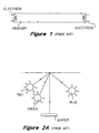
- Figure 1 shows such a tube fluorescent lamp.
- a large potential difference generated between the two electrodes at the ends of the tube breaks down a noble gas, such as argon, in the tube.
- Currents then conduct through the tube vaporizing and ionizing mercury droplets in the tube.
- mercury ions recombine after being excited, ultraviolet radiation is generated.
- the tube is coated by phosphors, which transform the incident ultraviolet radiation to visible light.
- a fluorescent lamp is commonly used as the light source in an office document scanner because of its relatively low cost relative to prior art alternative light sources.
- the fluorescent lamp has some shortcomings when used for this purpose.
- the fluorescent lamp is not a stable light source. It is an arc lamp, with light output highly dependent on the localized temperature dynamics of the arc, the noble gas and the vaporized mercury. Consequently, the light intensity from the lamp varies both spatially and temporally along the length of the lamp. Such variation degrades the accuracy of scanned images.
- the fluorescent lamp should be warmed-up prior to use, as the heat generated from the arc has to vaporize and uniformly distribute the otherwise liquid drops of mercury.
- the fluorescent lamp is quite bulky and should be shielded to protect the scanner sensor from heat and stray light.
- the problems are intensified in a color scanner as shown in Figure 2A.
- a color scanner as shown in Figure 2A.
- three different broadband illuminators as the source to cover the visible spectrum.
- each illuminator sequentially shines onto it. Reflections from each illuminator are measured to reconstruct the color of the area.
- fluorescent lamps are broadband devices.
- the phosphors in each lamp are selected to irradiate in the red, green or blue of the visible spectrum, so that the three lamps fully cover the visible spectrum.
- the three lamps are put into an optical system so that they all illuminate a common scan line on an object, and the reflected_light is measured by a sensor.
- This system works, but may be inaccurate, wasteful and complicated because, in addition to all the above-identified difficulties of fluorescent lamps, the phosphors in each lamp age at different rates. This can lead to color error.
- the light generated by each lamp is not directional. In scanning, one is looking at specific areas. The light that is not pointed towards those areas is wasted. In tact, such wasted light power usually tends to generate unwanted heat, which means that one needs to have thermal isolation.
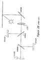
- Figure 2B shows another prior art method using a single white light fluorescent lamp as the source of a typical scanner.
- the reflected beam is split into different paths to be measured by sensors that are sensitive to different colors.
- the difference in sensitivity to different colors may be achieved by placing different filters over the same type of sensors. This method again incurs the weaknesses of a fluorescent lamp.
- lasers or light-emitting-diodes are not very suitable as broadband illuminators. This is because both lasers and LEDs are inherently narrow-band devices. If the source is made up of a red, a green and a blue LED, color error may occur for an object area that is not primarily red or green or blue.
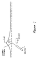
- Figure 3 illustrates one problem encountered by a very narrow source when it is used in a scanner.
- the medium scanned is planar, shown as dotted lines in Figure 3.
- a sensor As light shines onto the planar medium, diffused light will be reflected and measured by a sensor.
- a medium with a curved surface such as bound-printed subject matter close to the cusp of two adjacent pages. Due to the curvature of the medium, the light may impinge on a position quite different from the desired position; then the amount of the reflected diffused light reaching the sensor may be significantly reduced.
- One way to resolve the problem is to increase the power of the source and to widen the beam-width of the radiation through optics. However, this will increase the complexity and cost of the scanner.
- the present invention is on a broadband radiation source that is spatially and temporally uniform, with a beam-width more suitable to be used as an illuminating source for a scanner, and that is relatively inexpensive to build. Also, the invented solid-state electroluminescent element provides a broadband, directional, stable, rugged, efficient, compact source, which requires no warm-up time.
- an electroluminescent device capable of use as an illuminating source in a scanning apparatus, the device comprising a solid-state electroluminescent element, which comprises:
- a uniform radiation source is created for illuminating the medium.
- the bottom electrode is preferably a reflective electrode.
- the electroluminescent element can be more easily designed to be an illuminating source for a scanner.
- the top surface has a length of 22.8 cm (9 inches) and a width of 0.635 cm (a quarter of an inch).
- the source is very rugged because it can be made of solid-state layers on a variety of mechanically strong substrates, such as glass.
- the source is also very efficient because radiation is emitted over a controlled area, which substantially coincides with the object line to be scanned. Inherently, the source is stable over a broad temperature range. The temperature across the invention is fairly uniform, and there is no warm-up requirement.
- the light generated is both spatially and temporally uniform or homogenous because of the uniformity of the thin or thick-film process to make the device.
- the selected voltage source excites the dopant ions in the active layers; when the excited ions relax, radiation is generated.
- the selected voltage source excites the dopant ions in the active layers; when the excited ions relax, radiation is generated.
- the radiation emitted from different active layers centers around different frequencies so that the combined effect of the radiation has a desired spectral power distribution, such as white.
- an inductor is connected across the two electrodes of one of the above electroluminescent elements.
- the electroluminescent element and the inductor form a resonating circuit to increase the power efficiency of the element.
- the electroluminescent element is very rugged because it can be made of a thin-film stack on a glass substrate, a ceramic surface or other types of substrates 108. With light generated through electroluminescence, the source is very stable, with practically no non-uniform temperature rise or warm-up period. Moreover, the light generated and emitted from the top surface 112 is substantially uniform or homogenous both spatially and temporally because of the uniformity of the thin-film process in making the element.
- Prior art fluorescent lamps are bulky and cylindrical in shape. When the lamps illuminate the medium to be scanned, light radiates into many different directions. Energy is lost, generating heat for the environment. Thus, one has to thermally isolate the lamps.
- a flat and directional solid-state source greatly alleviates such problems.
- Figure 4B shows one arrangement with the stack including an active layer 150 and an insulating layer 152 which may be dielectric; and Figure 4C shows another arrangement with the stack 104 including an active layer 156 sandwiched between two insulating layers, 154 and 157.
- the voltage of the source creates excited dopant ions in the active layer. When the excited dopants relax, photon radiation is generated. By controlling the level and the frequency of the voltage, one can control the power level of the radiation emitted. Although some of the generated radiation may leak out from the edges, such as 114, of the element, most of the generated radiation emits from the top surface 112. This is because, typically, the area of top surface 112 is orders of magnitude greater than the areas occupied by the edges. Also, in order for some of the radiation to be emitted from the edges, they might have to travel through a long distance before reaching an edge. Before they reach an edge, they may have been attenuated, or may have already emitted from the top surface 112, through the transparent electrode 102. The amount of radiation emitted from the top surface can be increased by roughening either the top or the bottom surface. In fact, the amount of radiation can be increased by increasing the roughness of any interfacing surface between any of the layers described above, such as the interfacing surface 153.
- Figure 4D shows a preferred radiation generating stack 104 in accordance with a first embodiment of the present invention; it includes three active layers, 160, 162 and 164, between two insulating layers , 158 and 166.
- the radiation from each active layer centers around a frequency that is different from the other active layer. For example, one centers around blue-green, and another centers around red. When all the layers are excited, different radiation is combined to generate the radiation with a desired colour.
- Figure 4E shows another preferred embodiment with two electroluminescent elements, one on top of the other.
- One element 180 includes a transparent layer 168, a radiation generating stack 170 and another transparent layer 172; the second element 182 includes the transparent layer 172, a radiation generating stack 174 and a reflective electrode 176.
- the radiation from the two elements radiates around different frequencies so that the radiation of the combined effect is at a colour different from that of each individual element. Note that one can have more than two electroluminescent elements, one on top of the other.
- the active film is made of zinc sulphide doped with manganese; another type of active layer is made of strontium sulphide doped with cerium 3+ to emit radiation in the blue-green regions; a further type of active layer is strontium sulphide doped with europium 2+ to emit radiation 154 in the red region.
- a transparent electrode is made of indium tin oxide or zinc oxide of about 2000 Angstroms thick; a reflective electrode is made of aluminium of about 1000 Angstroms thick; an insulating layer is made of silicon-oxinitride of about 2000 Angstroms thick; and the active layer is about 1 micron thick.
- the element is about 22.8 cm (9 inches) long in the Y direction, and 0.635 cm (1/4 inch) wide in the X direction.
- the films are described as thin-films, they are not limited to very thin layers.
- the layers may be made by different techniques, such as by vapour-deposition or thick-film processes; and as an example, an insulating layer may be as thick as ten microns.
- one electrode is described as transparent and the other reflective, both electrodes may be transparent; in such an embodiment, radiation will be emitted from two surfaces.
- Figure 5 shows a preferred embodiment 204 with an electroluminescent element 200 and a sensor 202 in a scanner 206 scanning a medium 208.
- the width of the element can be 0.635 cm (1/4 inch) or more, a significant amount of radiation will impinge onto the medium, and reflected by the medium to be measured by the sensor 202. In some other preferred embodiments, the width of the element can be narrower.
- the senor used in the preferred embodiments also includes one or more optical elements.
- An optical element includes one or more lenses, prisms, mirrors and diffractive elements.
- Figure 6 shows a SELFOC lens 275, or a graded-index lens, for a sensor 277 in a scanner 281, with a scanning surface 279, which touches the medium to be scanned.
- the depth of focus of a typical SELFOC lens is about a few millimetres. So the lens should be close to the medium to be scanned, which is typically the case for the scanner inside a facsimile machine.
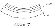
- Figure 7 shows a preferred electroluminescent element 475 that is curved to help focusing radiation emitted from the element 475 along a desired direction.
- each layer on top of the substrate 477 substantially replicates the curvature of the substrate 477.
- Each electroluminescent element has a capacitive effect.
- a preferred electroluminescent element 600 is connected to an inductor 602.
- the resonating effect of the circuit reduces the amount of power required to activate the element.
- the inductor may be the secondary winding of a transformer.
- a voltage source 604 can be coupled to the LC circuit to deliver power to the electroluminescent device by connecting the voltage source to the primary winding of the transformer.
- the frequency of the voltage source 604 should be equal to the resonant frequency of the LC circuit.
- the scanner described in the present invention may be a desk-top scanner or a portable scanner. It may be used as a stand-alone scanner, or it may be incorporated in a copier, a fax machine or the "erase bar" of an electrophotographic printer. Such instruments should be well-known to those skilled in the art, and will not be further described in this application. If the scanner is used for a typical A4 size paper 21.6 cm by 28 cm (8.5 inches by 11 inches), then the elements may need to be more than 21.6 cm (8.5 inches) in length.
- colour generation is achieved by three electroluminescent elements.
- colour generation can be achieved by two or more elements.
- FIG. 9 shows a preferred embodiment 700 with a reflective electrode 706 on top of a radiation generating stack 704, which is, in turn, on top of a transparent electrode 702. If one flips the preferred embodiment 700 upside down, the transparent electrode 702 will be on top. In the embodiment shown in Figure 9, the "top" surface 710 of the transparent electrode 702 is adjacent to a transparent substrate 708, such as glass.
- the electroluminescent element includes a transparent electrode and a reflective electrode.
- Figure 10 shows another preferred embodiment 800 with both electrodes being transparent.
- the embodiment 800 includes a first transparent electrode 802 with a first surface 801, a radiation generating stack 804, a second transparent electrode 806 with a second surface 807, and a transparent substrate 808.
- Most of the emitted radiation generated is emitted from both the first and the second surfaces.
- the emitted radiation is substantially uniform across both the first and the second surfaces to create a uniform radiation source.
- One way to direct the emitted radiation towards one direction is to have two mirrors, 810 and 812, to reflect the emitted radiation.
Landscapes
- Engineering & Computer Science (AREA)
- Multimedia (AREA)
- Signal Processing (AREA)
- Physics & Mathematics (AREA)
- General Health & Medical Sciences (AREA)
- Electromagnetism (AREA)
- Health & Medical Sciences (AREA)
- Toxicology (AREA)
- Artificial Intelligence (AREA)
- Computer Vision & Pattern Recognition (AREA)
- General Physics & Mathematics (AREA)
- Theoretical Computer Science (AREA)
- Facsimile Scanning Arrangements (AREA)
- Electroluminescent Light Sources (AREA)
- Light Sources And Details Of Projection-Printing Devices (AREA)
Description
- The present invention relates generally to electroluminescent devices and more particularly to using an electroluminescent device as a radiation source for a scanner.
- For a number of years, the best light source for scanning a document has been a fluorescent lamp. Figure 1 shows such a tube fluorescent lamp. A large potential difference generated between the two electrodes at the ends of the tube breaks down a noble gas, such as argon, in the tube. Currents then conduct through the tube vaporizing and ionizing mercury droplets in the tube. When the mercury ions recombine after being excited, ultraviolet radiation is generated. The tube is coated by phosphors, which transform the incident ultraviolet radiation to visible light.
- A fluorescent lamp is commonly used as the light source in an office document scanner because of its relatively low cost relative to prior art alternative light sources. However, the fluorescent lamp has some shortcomings when used for this purpose. Most notably, the fluorescent lamp is not a stable light source. It is an arc lamp, with light output highly dependent on the localized temperature dynamics of the arc, the noble gas and the vaporized mercury. Consequently, the light intensity from the lamp varies both spatially and temporally along the length of the lamp. Such variation degrades the accuracy of scanned images. Also, the fluorescent lamp should be warmed-up prior to use, as the heat generated from the arc has to vaporize and uniformly distribute the otherwise liquid drops of mercury. In addition, the fluorescent lamp is quite bulky and should be shielded to protect the scanner sensor from heat and stray light.
- The problems are intensified in a color scanner as shown in Figure 2A. In such a scanner, one typically needs three different broadband illuminators as the source to cover the visible spectrum. To scan the color of an area, each illuminator sequentially shines onto it. Reflections from each illuminator are measured to reconstruct the color of the area.
- Normally, fluorescent lamps are broadband devices. Typically, the phosphors in each lamp are selected to irradiate in the red, green or blue of the visible spectrum, so that the three lamps fully cover the visible spectrum. In a prior art embodiment, the three lamps are put into an optical system so that they all illuminate a common scan line on an object, and the reflected_light is measured by a sensor. This system works, but may be inaccurate, wasteful and complicated because, in addition to all the above-identified difficulties of fluorescent lamps, the phosphors in each lamp age at different rates. This can lead to color error. Also, as shown in Figure 2A, the light generated by each lamp is not directional. In scanning, one is looking at specific areas. The light that is not pointed towards those areas is wasted. In tact, such wasted light power usually tends to generate unwanted heat, which means that one needs to have thermal isolation.
- Figure 2B shows another prior art method using a single white light fluorescent lamp as the source of a typical scanner. In this example, the reflected beam is split into different paths to be measured by sensors that are sensitive to different colors. The difference in sensitivity to different colors may be achieved by placing different filters over the same type of sensors. This method again incurs the weaknesses of a fluorescent lamp.
- Note that lasers or light-emitting-diodes (LEDs) are not very suitable as broadband illuminators. This is because both lasers and LEDs are inherently narrow-band devices. If the source is made up of a red, a green and a blue LED, color error may occur for an object area that is not primarily red or green or blue.
- One excellent solution to the above problems has been proposed in a European patent application, EP 0 721 293 A1 titled, "Edge Emitter", forming part of the prior art only with respect to Article 54 (3) EPC, which describes already the prior art as shown in Fig. 1, 2A and 2B. That application describes different types of solid-state electroluminescent devices, all with edges. Each of them provides a broadband, directional, solid-state source that is stable, spatially and temporally uniform, rugged, efficient, compact and requires practically no warm-up period. The radiation generated emits from an edge of the device. If the devices are used in a scanner, it is very important for the devices to be stable spatially and temporally. In order to find out what one has scanned, typically, one compares the reflected radiation from the scanned surface with the incident radiation. A scanner would be much more expensive to accommodate for spatial and temporal variations in the incident radiation. Also, the devices in the European application are very efficient because the radiation is emitted from edges over narrow lines. However, in some applications, one may not want to have the radiation confined too narrow an area.
- Similar edge emitters are disclosed in EP 0 372 942 A2 and EP 0 408 231 A. A radiation edge emitter is discribed in EP 0 710 050 A1 forming part of the prior art only in the context of Article 54 (3) EPC.
- Figure 3 illustrates one problem encountered by a very narrow source when it is used in a scanner. Typically, the medium scanned is planar, shown as dotted lines in Figure 3. As light shines onto the planar medium, diffused light will be reflected and measured by a sensor. However, in many situations, one has to scan a medium with a curved surface, such as bound-printed subject matter close to the cusp of two adjacent pages. Due to the curvature of the medium, the light may impinge on a position quite different from the desired position; then the amount of the reflected diffused light reaching the sensor may be significantly reduced. One way to resolve the problem is to increase the power of the source and to widen the beam-width of the radiation through optics. However, this will increase the complexity and cost of the scanner.
- It should be apparent from the foregoing that there is still a need for a broadband radiation source that is spatially and temporally uniform, with a beam-width more suitable to be used in a scanner, and that is relatively inexpensive to build.
- The present invention is on a broadband radiation source that is spatially and temporally uniform, with a beam-width more suitable to be used as an illuminating source for a scanner, and that is relatively inexpensive to build. Also, the invented solid-state electroluminescent element provides a broadband, directional, stable, rugged, efficient, compact source, which requires no warm-up time.
- According to the present invention, there is provided an electroluminescent device capable of use as an illuminating source in a scanning apparatus, the device comprising a solid-state electroluminescent element, which comprises:
- a transparent electrode with a top surface;
- a radiation generating stack under the transparent electrode; and
- a second electrode under the radiation generating stack, the second electrode having a bottom surface;
- such that:
- radiation is generated from the radiation generating stack when a selected voltage source is coupled across the electrodes;
- the device being characterised in that said stack comprises a plurality of active layers between the electrodes, the radiation from the layers being centred on different frequencies, and in that the arrangement is such that most of the radiation generated is emitted either from the top surface or from the top and the bottom surface, and the emitted radiation is substantially uniform at least across the top surface of the transparent electrode to create a uniform radiation source for illumination.
-
- When a scanner using the electroluminescent device scans a medium, a uniform radiation source is created for illuminating the medium.
- Unless stated otherwise, the bottom electrode is preferably a reflective electrode. With radiation emitting from the top surface instead of from edges, the electroluminescent element can be more easily designed to be an illuminating source for a scanner. One can change the beam-width of the emitted radiation by changing the desired size of the top surface of the transparent electrode. In one embodiment, the top surface has a length of 22.8 cm (9 inches) and a width of 0.635 cm (a quarter of an inch).
- The source is very rugged because it can be made of solid-state layers on a variety of mechanically strong substrates, such as glass. The source is also very efficient because radiation is emitted over a controlled area, which substantially coincides with the object line to be scanned. Inherently, the source is stable over a broad temperature range. The temperature across the invention is fairly uniform, and there is no warm-up requirement. Moreover, the light generated is both spatially and temporally uniform or homogenous because of the uniformity of the thin or thick-film process to make the device.
- The selected voltage source excites the dopant ions in the active layers; when the excited ions relax, radiation is generated. By careful selection of the dopant ions, one can tailor the bandwidth of the emission to increase the colorimetric accuracy of the source. The radiation emitted from different active layers centers around different frequencies so that the combined effect of the radiation has a desired spectral power distribution, such as white.
- In one embodiment, an inductor is connected across the two electrodes of one of the above electroluminescent elements. The electroluminescent element and the inductor form a resonating circuit to increase the power efficiency of the element.
- Other aspects and advantages of the present invention will become apparent from the following detailed description, which, when taken in conjunction with the accompanying drawings, illustrates by way of example different embodiments of the invention. In the drawings:
- Figure 1 shows a prior art tube fluorescent lamp.
- Figures 2A-B show prior art colour sources using lamps.
- Figure 3 shows a source and a sensor in a scanner scanning two pages from a book.
- Figures 4A-C show different electroluminescent devices useful in explaining the present invention.
- Figures 4D & 4E show different preferred embodiments of the present invention.
- Figure 5 shows a preferred embodiment scanning a medium.
- Figure 6 shows a preferred embodiment with lens structure on a sensor.
- Figure 7 shows a preferred electroluminescent element with a curved top surface.
- Figure 8 shows a preferred electroluminescent element connected to an inductor.
- Figure 9 shows a preferred electroluminescent element with a transparent electrode adjacent to a transparent substrate.
- Figure 10 shows a preferred electroluminescent element with two transparent electrodes.
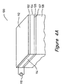
- Figure 4A shows a
preferred electroluminescent element 100 useful in explaining the present invention. Theelement 100 includes atransparent electrode 102 with atop surface 112, aradiation generating stack 104 and asecond electrode 106, with abottom surface 107. The electrodes are connected to avoltage source 110. Unless stated otherwise, thesecond electrode 106 is preferably a reflective electrode. -
- The electroluminescent element is very rugged because it can be made of a thin-film stack on a glass substrate, a ceramic surface or other types of
substrates 108. With light generated through electroluminescence, the source is very stable, with practically no non-uniform temperature rise or warm-up period. Moreover, the light generated and emitted from thetop surface 112 is substantially uniform or homogenous both spatially and temporally because of the uniformity of the thin-film process in making the element. - Another benefit of the element is that it is flat and directional. Prior art fluorescent lamps are bulky and cylindrical in shape. When the lamps illuminate the medium to be scanned, light radiates into many different directions. Energy is lost, generating heat for the environment. Thus, one has to thermally isolate the lamps. A flat and directional solid-state source greatly alleviates such problems.
- Different arrangements are suitable for the
radiation generating stack 104. Figure 4B shows one arrangement with the stack including anactive layer 150 and an insulating layer 152 which may be dielectric; and Figure 4C shows another arrangement with thestack 104 including anactive layer 156 sandwiched between two insulating layers, 154 and 157. - The voltage of the source creates excited dopant ions in the active layer. When the excited dopants relax, photon radiation is generated. By controlling the level and the frequency of the voltage, one can control the power level of the radiation emitted. Although some of the generated radiation may leak out from the edges, such as 114, of the element, most of the generated radiation emits from the
top surface 112. This is because, typically, the area oftop surface 112 is orders of magnitude greater than the areas occupied by the edges. Also, in order for some of the radiation to be emitted from the edges, they might have to travel through a long distance before reaching an edge.
Before they reach an edge, they may have been attenuated, or may have already emitted from thetop surface 112, through thetransparent electrode 102.
The amount of radiation emitted from the top surface can be increased by roughening either the top or the bottom surface. In fact, the amount of radiation can be increased by increasing the roughness of any interfacing surface between any of the layers described above, such as theinterfacing surface 153. - Figure 4D shows a preferred
radiation generating stack 104 in accordance with a first embodiment of the present invention; it includes three active layers, 160, 162 and 164, between two insulating layers , 158 and 166. Typically, the radiation from each active layer centers around a frequency that is different from the other active layer. For example, one centers around blue-green, and another centers around red. When all the layers are excited, different radiation is combined to generate the radiation with a desired colour. - Figure 4E shows another preferred embodiment with two electroluminescent elements, one on top of the other. One
element 180 includes atransparent layer 168, aradiation generating stack 170 and anothertransparent layer 172; thesecond element 182 includes thetransparent layer 172, aradiation generating stack 174 and areflective electrode 176. The radiation from the two elements radiates around different frequencies so that the radiation of the combined effect is at a colour different from that of each individual element. Note that one can have more than two electroluminescent elements, one on top of the other. - In one example, the active film is made of zinc sulphide doped with manganese; another type of active layer is made of strontium sulphide doped with cerium3+ to emit radiation in the blue-green regions; a further type of active layer is strontium sulphide doped with europium2+ to emit
radiation 154 in the red region. - In one working embodiment, a transparent electrode is made of indium tin oxide or zinc oxide of about 2000 Angstroms thick; a reflective electrode is made of aluminium of about 1000 Angstroms thick; an insulating layer is made of silicon-oxinitride of about 2000 Angstroms thick; and the active layer is about 1 micron thick. The element is about 22.8 cm (9 inches) long in the Y direction, and 0.635 cm (1/4 inch) wide in the X direction.
- Although the films are described as thin-films, they are not limited to very thin layers. The layers may be made by different techniques, such as by vapour-deposition or thick-film processes; and as an example, an insulating layer may be as thick as ten microns. Also, although one electrode is described as transparent and the other reflective, both electrodes may be transparent; in such an embodiment, radiation will be emitted from two surfaces.
- Figure 5 shows a
preferred embodiment 204 with anelectroluminescent element 200 and asensor 202 in ascanner 206 scanning a medium 208. As described above, in some preferred embodiments, the width of the element can be 0.635 cm (1/4 inch) or more, a significant amount of radiation will impinge onto the medium, and reflected by the medium to be measured by thesensor 202. In some other preferred embodiments, the width of the element can be narrower. - In many applications, the sensor used in the preferred embodiments also includes one or more optical elements. An optical element includes one or more lenses, prisms, mirrors and diffractive elements. Figure 6 shows a
SELFOC lens 275, or a graded-index lens, for asensor 277 in ascanner 281, with ascanning surface 279, which touches the medium to be scanned. The depth of focus of a typical SELFOC lens is about a few millimetres. So the lens should be close to the medium to be scanned, which is typically the case for the scanner inside a facsimile machine. - Figure 7 shows a
preferred electroluminescent element 475 that is curved to help focusing radiation emitted from theelement 475 along a desired direction. In this embodiment, each layer on top of thesubstrate 477 substantially replicates the curvature of thesubstrate 477. - Each electroluminescent element has a capacitive effect. One way to increase the power efficiency of the element is shown in Figure 8, where a
preferred electroluminescent element 600 is connected to aninductor 602. The resonating effect of the circuit reduces the amount of power required to activate the element. The inductor may be the secondary winding of a transformer. Then avoltage source 604 can be coupled to the LC circuit to deliver power to the electroluminescent device by connecting the voltage source to the primary winding of the transformer. The frequency of thevoltage source 604 should be equal to the resonant frequency of the LC circuit. - The scanner described in the present invention may be a desk-top scanner or a portable scanner. It may be used as a stand-alone scanner, or it may be incorporated in a copier, a fax machine or the "erase bar" of an electrophotographic printer. Such instruments should be well-known to those skilled in the art, and will not be further described in this application. If the scanner is used for a typical A4 size paper 21.6 cm by 28 cm (8.5 inches by 11 inches), then the elements may need to be more than 21.6 cm (8.5 inches) in length.
- In the above descriptions, typically, colour generation is achieved by three electroluminescent elements. However, it should be obvious to those skilled in the art that colour generation can be achieved by two or more elements.
- The surface covering the transparent electrode is typically defined as the top surface. However, top and bottom are relative terms. Figure 9 shows a
preferred embodiment 700 with areflective electrode 706 on top of aradiation generating stack 704, which is, in turn, on top of atransparent electrode 702. If one flips thepreferred embodiment 700 upside down, thetransparent electrode 702 will be on top. In the embodiment shown in Figure 9, the "top"surface 710 of thetransparent electrode 702 is adjacent to atransparent substrate 708, such as glass. - In most of the embodiments described, the electroluminescent element includes a transparent electrode and a reflective electrode. Figure 10 shows another
preferred embodiment 800 with both electrodes being transparent. Theembodiment 800 includes a firsttransparent electrode 802 with afirst surface 801, aradiation generating stack 804, a secondtransparent electrode 806 with asecond surface 807, and atransparent substrate 808. Most of the emitted radiation generated is emitted from both the first and the second surfaces. The emitted radiation is substantially uniform across both the first and the second surfaces to create a uniform radiation source. One way to direct the emitted radiation towards one direction is to have two mirrors, 810 and 812, to reflect the emitted radiation.
Claims (5)
- An electroluminescent device capable of use as an illuminating source in a scanning apparatus, the device comprising a solid-state electroluminescent element (100), which comprises:a transparent electrode (102) with a top surface (112) ;a radiation generating stack (104) under the transparent electrode; anda second electrode (106) under the radiation generating stack (104), the second electrode having a bottom surface;such that:radiation is generated from the radiation generating stack (104) when a selected voltage source (116) is coupled across the electrodes;the device being characterised in that said stack (104) comprises a plurality of active layers (160, 162, 164; 170, 174) between the electrodes (102, 106), the radiation from the layers being centred on different frequencies, and in that the arrangement is such that most of the radiation generated is emitted either from the top surface or from the top and the bottom surface, and the emitted radiation is substantially uniform at least across the top surface of the transparent electrode to create a uniform radiation source for illumination.
- An electroluminescent device as recited in claim 1, wherein the second electrode (106) is a reflective electrode.
- An electroluminescent device as recited in claim 1 or 2, wherein the active layers (160, 162, 164) are arranged between a first dielectric layer (158) and a second dielectric layer (166).
- An electroluminescent device as recited in claim 1, further comprising:a sensor for measuring the radiation reflected from a medium scanned by the apparatus; and an optical element to direct the radiation reflected from the medium to be measured by the sensor.
- Scanning apparatus for a medium, comprising an electroluminescent device as claimed in any preceding claim.
Applications Claiming Priority (2)
| Application Number | Priority Date | Filing Date | Title |
|---|---|---|---|
| US479376 | 1995-06-07 | ||
| US08/479,376 US5598067A (en) | 1995-06-07 | 1995-06-07 | Electroluminescent device as a source for a scanner |
Publications (3)
| Publication Number | Publication Date |
|---|---|
| EP0748145A2 EP0748145A2 (en) | 1996-12-11 |
| EP0748145A3 EP0748145A3 (en) | 1998-10-14 |
| EP0748145B1 true EP0748145B1 (en) | 2003-06-04 |
Family
ID=23903748
Family Applications (1)
| Application Number | Title | Priority Date | Filing Date |
|---|---|---|---|
| EP96304140A Expired - Lifetime EP0748145B1 (en) | 1995-06-07 | 1996-06-05 | Electroluminescent device as a source for a scanner |
Country Status (6)
| Country | Link |
|---|---|
| US (1) | US5598067A (en) |
| EP (1) | EP0748145B1 (en) |
| JP (1) | JPH0927886A (en) |
| KR (1) | KR100439390B1 (en) |
| DE (1) | DE69628503T2 (en) |
| TW (1) | TW410013U (en) |
Families Citing this family (13)
| Publication number | Priority date | Publication date | Assignee | Title |
|---|---|---|---|---|
| US6118555A (en) * | 1995-03-02 | 2000-09-12 | Canon Kabushiki Kaisha | Image reading apparatus having a light source including a fluorescent lamp |
| US5671059A (en) * | 1995-09-21 | 1997-09-23 | Hewlett-Packard Company | Electroluminescent color device |
| US6607277B2 (en) * | 1996-09-24 | 2003-08-19 | Seiko Epson Corporation | Projector display comprising light source units |
| JP4267136B2 (en) * | 1998-09-25 | 2009-05-27 | 富士フイルム株式会社 | Radiation image detection and reading device |
| US6396218B1 (en) | 2000-10-03 | 2002-05-28 | Xerox Corporation | Multisegment electroluminescent source for a scanner |
| JP3979072B2 (en) * | 2001-03-19 | 2007-09-19 | 松下電器産業株式会社 | EL lamp manufacturing method |
| US6953735B2 (en) * | 2001-12-28 | 2005-10-11 | Semiconductor Energy Laboratory Co., Ltd. | Method for fabricating a semiconductor device by transferring a layer to a support with curvature |
| JP3956963B2 (en) * | 2004-08-16 | 2007-08-08 | コニカミノルタビジネステクノロジーズ株式会社 | Image reading device |
| JP2006060528A (en) * | 2004-08-20 | 2006-03-02 | Ricoh Co Ltd | Contact image sensor, image reading apparatus, image forming apparatus |
| JP2007013913A (en) * | 2005-05-30 | 2007-01-18 | Toyota Industries Corp | Lighting unit and original-reading apparatus |
| JP2007201826A (en) * | 2006-01-26 | 2007-08-09 | Ricoh Co Ltd | Image reading apparatus and image forming apparatus |
| JP4798050B2 (en) * | 2007-04-03 | 2011-10-19 | 株式会社豊田自動織機 | Light source for scanner |
| JP4766066B2 (en) | 2008-03-14 | 2011-09-07 | コニカミノルタビジネステクノロジーズ株式会社 | Image reading apparatus and light source |
Family Cites Families (11)
| Publication number | Priority date | Publication date | Assignee | Title |
|---|---|---|---|---|
| US5043631A (en) * | 1988-08-23 | 1991-08-27 | Westinghouse Electric Corp. | Thin film electroluminescent edge emitter structure on a silicon substrate |
| US5043715A (en) * | 1988-12-07 | 1991-08-27 | Westinghouse Electric Corp. | Thin film electroluminescent edge emitter structure with optical lens and multi-color light emission systems |
| FI895852A0 (en) * | 1988-12-07 | 1989-12-07 | Westinghouse Electric Corp | TUNN FILM ELECTROLUMINESCENT. KANTEMITTERSTRUKTUR MED INBYGGT OPTISKT LINSSYSTEM. |
| US5101137A (en) * | 1989-07-10 | 1992-03-31 | Westinghouse Electric Corp. | Integrated tfel flat panel face and edge emitter structure producing multiple light sources |
| US5118987A (en) * | 1989-11-13 | 1992-06-02 | Westinghouse Electric Corp. | Multi-layer structure and method of constructing the same for providing tfel edge emitter modules |
| US5043632A (en) * | 1990-04-13 | 1991-08-27 | Westinghouse Electric Corp. | TFEL edge emitter structure with uniform light emission filter |
| US5252895A (en) * | 1991-05-09 | 1993-10-12 | Westinghouse Electric Corp. | TFEL edge emitter structure with light emitting face at angle greater than ninety degrees to substrate street |
| US5258690A (en) * | 1991-05-23 | 1993-11-02 | Westinghouse Electric Corp. | TFEL edge emitter module with hermetically-sealed and refractive index-matched solid covering over light-emitting face |
| US5384577A (en) * | 1992-05-21 | 1995-01-24 | Motorola, Inc. | Combination display backlight and light sensor |
| EP0710050A1 (en) * | 1994-10-27 | 1996-05-01 | Hewlett-Packard Company | Radiation edge emitter |
| US5525866A (en) * | 1995-01-06 | 1996-06-11 | Mueller; Gerd O. | Edge emitter as a directional line source |
-
1995
- 1995-06-07 US US08/479,376 patent/US5598067A/en not_active Expired - Lifetime
-
1996
- 1996-04-25 TW TW087219131U patent/TW410013U/en unknown
- 1996-06-04 JP JP8141830A patent/JPH0927886A/en active Pending
- 1996-06-05 DE DE69628503T patent/DE69628503T2/en not_active Expired - Fee Related
- 1996-06-05 EP EP96304140A patent/EP0748145B1/en not_active Expired - Lifetime
- 1996-06-05 KR KR1019960020149A patent/KR100439390B1/en not_active IP Right Cessation
Also Published As
| Publication number | Publication date |
|---|---|
| KR100439390B1 (en) | 2004-08-04 |
| EP0748145A3 (en) | 1998-10-14 |
| JPH0927886A (en) | 1997-01-28 |
| EP0748145A2 (en) | 1996-12-11 |
| DE69628503D1 (en) | 2003-07-10 |
| US5598067A (en) | 1997-01-28 |
| TW410013U (en) | 2000-10-21 |
| DE69628503T2 (en) | 2004-05-13 |
| KR970002736A (en) | 1997-01-28 |
Similar Documents
| Publication | Publication Date | Title |
|---|---|---|
| EP0748145B1 (en) | Electroluminescent device as a source for a scanner | |
| JP4988586B2 (en) | LED lighting device with optical feedback by image mapping on segmented photosensor | |
| JP3908786B2 (en) | Lighting system for Indicia OCR on board | |
| US5525866A (en) | Edge emitter as a directional line source | |
| US20020109866A1 (en) | Film scanner with uniformized infrared light by utilizing a cold cathode fluorescent lamp | |
| US6760139B2 (en) | Optical image scanner with lens arrays that are non-perpendicular to the image being scanned | |
| JP3509551B2 (en) | Light source device with external electrode type discharge lamp | |
| JP2000115470A (en) | Original reader | |
| US6396218B1 (en) | Multisegment electroluminescent source for a scanner | |
| JPH08293620A (en) | Image reading device | |
| US5596360A (en) | Image reading apparatus with a half mirror | |
| US6900593B2 (en) | Light source and image reading device using the same | |
| EP0174094B1 (en) | Imaging system using a full frame illumination array | |
| EP0342607B1 (en) | Color image input unit having a rare gas cathode discharge tube | |
| JP2984146B2 (en) | Light source for contact image sensor | |
| JP2003309707A (en) | Image reader | |
| JPH1198331A (en) | Image irradiation device and image reader using the device | |
| JPH0879446A (en) | Image input device | |
| JP2003348297A (en) | Contact type image sensor and image reader | |
| JPH06194596A (en) | Illuminator | |
| JPH05227377A (en) | Original lighting light source | |
| JPH01264164A (en) | Fluorescent tube and color image reader | |
| GB2414618A (en) | Optical image scanner with lens arrays that are non-perpendicular to the image being scanned | |
| JPH0766936A (en) | Contact type image sensor | |
| JPS61284163A (en) | Illuminating device with fluorescent tube for original reading |
Legal Events
| Date | Code | Title | Description |
|---|---|---|---|
| PUAI | Public reference made under article 153(3) epc to a published international application that has entered the european phase |
Free format text: ORIGINAL CODE: 0009012 |
|
| AK | Designated contracting states |
Kind code of ref document: A2 Designated state(s): DE FR GB |
|
| PUAL | Search report despatched |
Free format text: ORIGINAL CODE: 0009013 |
|
| AK | Designated contracting states |
Kind code of ref document: A3 Designated state(s): DE FR GB |
|
| 17P | Request for examination filed |
Effective date: 19990414 |
|
| 17Q | First examination report despatched |
Effective date: 19991103 |
|
| RAP1 | Party data changed (applicant data changed or rights of an application transferred) |
Owner name: HEWLETT-PACKARD COMPANY, A DELAWARE CORPORATION |
|
| GRAH | Despatch of communication of intention to grant a patent |
Free format text: ORIGINAL CODE: EPIDOS IGRA |
|
| GRAH | Despatch of communication of intention to grant a patent |
Free format text: ORIGINAL CODE: EPIDOS IGRA |
|
| GRAA | (expected) grant |
Free format text: ORIGINAL CODE: 0009210 |
|
| AK | Designated contracting states |
Designated state(s): DE FR GB |
|
| REG | Reference to a national code |
Ref country code: GB Ref legal event code: FG4D |
|
| REF | Corresponds to: |
Ref document number: 69628503 Country of ref document: DE Date of ref document: 20030710 Kind code of ref document: P |
|
| ET | Fr: translation filed | ||
| PLBE | No opposition filed within time limit |
Free format text: ORIGINAL CODE: 0009261 |
|
| STAA | Information on the status of an ep patent application or granted ep patent |
Free format text: STATUS: NO OPPOSITION FILED WITHIN TIME LIMIT |
|
| 26N | No opposition filed |
Effective date: 20040305 |
|
| PGFP | Annual fee paid to national office [announced via postgrant information from national office to epo] |
Ref country code: DE Payment date: 20050801 Year of fee payment: 10 |
|
| PG25 | Lapsed in a contracting state [announced via postgrant information from national office to epo] |
Ref country code: DE Free format text: LAPSE BECAUSE OF NON-PAYMENT OF DUE FEES Effective date: 20070103 |
|
| PGFP | Annual fee paid to national office [announced via postgrant information from national office to epo] |
Ref country code: GB Payment date: 20070628 Year of fee payment: 12 |
|
| PGFP | Annual fee paid to national office [announced via postgrant information from national office to epo] |
Ref country code: FR Payment date: 20070618 Year of fee payment: 12 |
|
| GBPC | Gb: european patent ceased through non-payment of renewal fee |
Effective date: 20080605 |
|
| REG | Reference to a national code |
Ref country code: FR Ref legal event code: ST Effective date: 20090228 |
|
| PG25 | Lapsed in a contracting state [announced via postgrant information from national office to epo] |
Ref country code: GB Free format text: LAPSE BECAUSE OF NON-PAYMENT OF DUE FEES Effective date: 20080605 |
|
| PG25 | Lapsed in a contracting state [announced via postgrant information from national office to epo] |
Ref country code: FR Free format text: LAPSE BECAUSE OF NON-PAYMENT OF DUE FEES Effective date: 20080630 |