EP0746185B1 - Circuit de surveillance de l'état de functionnement d'un système à deux lampes - Google Patents
Circuit de surveillance de l'état de functionnement d'un système à deux lampes Download PDFInfo
- Publication number
- EP0746185B1 EP0746185B1 EP95108385A EP95108385A EP0746185B1 EP 0746185 B1 EP0746185 B1 EP 0746185B1 EP 95108385 A EP95108385 A EP 95108385A EP 95108385 A EP95108385 A EP 95108385A EP 0746185 B1 EP0746185 B1 EP 0746185B1
- Authority
- EP
- European Patent Office
- Prior art keywords
- control circuit
- lamp
- transistor
- voltage
- circuit
- Prior art date
- Legal status (The legal status is an assumption and is not a legal conclusion. Google has not performed a legal analysis and makes no representation as to the accuracy of the status listed.)
- Expired - Lifetime
Links
Images

Classifications
-
- H—ELECTRICITY
- H05—ELECTRIC TECHNIQUES NOT OTHERWISE PROVIDED FOR
- H05B—ELECTRIC HEATING; ELECTRIC LIGHT SOURCES NOT OTHERWISE PROVIDED FOR; CIRCUIT ARRANGEMENTS FOR ELECTRIC LIGHT SOURCES, IN GENERAL
- H05B41/00—Circuit arrangements or apparatus for igniting or operating discharge lamps
- H05B41/14—Circuit arrangements
- H05B41/26—Circuit arrangements in which the lamp is fed by power derived from dc by means of a converter, e.g. by high-voltage dc
- H05B41/28—Circuit arrangements in which the lamp is fed by power derived from dc by means of a converter, e.g. by high-voltage dc using static converters
- H05B41/282—Circuit arrangements in which the lamp is fed by power derived from dc by means of a converter, e.g. by high-voltage dc using static converters with semiconductor devices
- H05B41/285—Arrangements for protecting lamps or circuits against abnormal operating conditions
- H05B41/2851—Arrangements for protecting lamps or circuits against abnormal operating conditions for protecting the circuit against abnormal operating conditions
- H05B41/2855—Arrangements for protecting lamps or circuits against abnormal operating conditions for protecting the circuit against abnormal operating conditions against abnormal lamp operating conditions
Definitions
- the invention relates to a circuit arrangement according to the preamble of claim 1.
- Luminaires often not only have a single fluorescent lamp, so it is not uncommon with a single electronic Ballast at least two lamp circuits to supply together.
- the well-known Circuit arrangement has a monitoring device for Monitoring the lamp circuits for a fault condition, at the high ignition voltage inadmissibly longer than one predefined period of time is pending. This can happen if one fluorescent lamps at the end of their service life are no longer free of defects ignites or leaks. This error condition determined, the monitoring device switches on Inverter of the electronic ballast from and prevents the ignition voltage from being present again. Thereby will of course also each of the connected, operable per se Fluorescent lamps switched off.
- EP-B1-0 146 683 The circuit arrangement known from EP-B1-0 146 683 can be seen the disadvantage that the electronic ballast turns off, although z. B. only a single fluorescent lamp is broken and fluorescent lamps still working properly would be operational.
- One of EP-A-0 overcomes this disadvantage 558 772 known circuit arrangement for operating several Fluorescent lamps with a ballast. She also owns to the monitoring device mentioned between the lamp chokes and the fluorescent lamps arranged Switching device with which the lamp circuits share to only one of the lamp chokes depending on one Fault condition can be switched on in the case of one of the fluorescent lamps Ignition voltage longer than a predetermined period of time pending. This period is shorter than that Delay in response of the monitoring device.
- the known switching device is designed to be resettable, so that when the faulty fluorescent lamp is removed deactivated itself and falls back into its rest position. To the criterion is used that when the faulty, but until then on the lamp filaments still live fluorescent lamp the holding current of the switching device is halved. The switching device detects this Change and fall back to the rest position. After changing the lamp is thus automatically back to normal operating status manufactured in which both fluorescent lamps burn, without the electronic ballast being switched off ought to.
- the known circuit arrangement is quite advantageous because they are in a multi-lamp electronic ballast the unimpeded operation of functional lamp circuits also enabled if there is a fault in one of the connected Lamp circuits occur.
- the design of the known Circuit arrangement has the disadvantage that you Functional principle realized with the help of a predetermined time grid is, the boundary conditions of which are critical. It is obvious to a person skilled in the art that the response delay the monitoring device operating in the start / stop mode should not be chosen too large because one too Long exposure to high ignition voltage in the event of failure of all lamp circuits is unfavorable. On the other hand, it should be before Switching device to be activated is not premature switch to lamp operation on only one lamp choke, but in turn have switched before the inverter of the electronic ballast is completely switched off.
- the present invention is therefore based on the object based on the considerations underlying the known solution a further embodiment of a circuit arrangement of the type mentioned at the beginning with which the Advantages of the known solution can be achieved without it Having to accept disadvantages.
- the solution according to the invention is based on the idea that the starting behavior of a functional fluorescent lamp although it runs in a certain time grid and that a sequential Sequence of circuit measures in one of the possible and introductory fault cases of an unwanted ignition or ignitable fluorescent lamp is useful to at least the continued operation of functional fluorescent lamps ensure, but it is not necessary also the error monitoring must be adapted to it To force time grid.
- the solution according to the invention defines one sequential sequence in the detection of the circuit states in the event of a lamp failure, the controller sets the corresponding circuit states, however, in contrast to previously known solutions are not based on a predetermined time grid. Rather, the individual monitoring steps are carried out by the course or the instantaneous state of the ignition voltage derived as the state of charge of a storage capacitor is reproduced.
- the control circuit as well as the Monitoring circuitry are different with voltage dependent Thresholds for capacitor charging, so that they are waiting one after another for too long respond to high ignition voltage.
- the solution according to the invention is therefore reliable, but is still circuitry easier and cheaper to manufacture than the known solution.
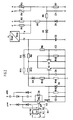
- Whose output voltage is offered an inverter 3, which is a high-frequency, pulse-shaped Output voltage uhb gives.
- Inverter 3 are the actual lamp circuits switched on. They contain two lamp chokes DR1 and DR2, those in the normal operating mode shown in Figure 1 each with one of the filaments of the two fluorescent lamps LL1 and LL2 are connected.
- Ignition capacitors CZ1 or CZ2 switched.
- the lamp circuits is also a monitoring circuit 4 assigned, which detects a faulty operating state, in which the high ignition voltage at at least one of the Fluorescent lamps LL1 or LL2 pending for too long and then turns off the inverter 3.
- the only monitoring criterion is however a long queue of high Ignition voltage, so that the monitoring circuit 4 switches Inverters 3 always off, if only one of the Fluorescent lamps LL1 or LL2 faulty if the filaments are intact works, d. H. cannot be ignited.
- Switch S1 provided with a changeover contact s.
- a control circuit 5 is assigned to this switch S1 is integrated in the lamp circuits and the operating function of fluorescent lamps LL1 and LL2 detected.
- the control circuit 5 detects an operating state at which the lamp ignition voltage on one of the fluorescent lamps LL1 or LL2 is pending longer than specified, in any case before the monitoring circuit 4 responds. If this becomes faulty Operating state determined, the control circuit switches 5 the switch S1 around. The changeover contact disconnects s one of the lamp circuits and connects this lamp circuit parallel to the other to the exit only one of the two lamp chokes, e.g. B. DR1. So two series resonance circles one formed in which the two Ignition capacitors CZ1 and CZ2 are parallel to each other.
- the control circuit 5 is designed so that it is resolved after resets the error itself, d. H. as soon as the defective fluorescent lamp LL1 or LL2 is removed. By resetting the control circuit 5 also becomes the switch S1 again in the circuit state shown in FIG. 1 switched, with which the normal operating state is restored and the newly installed fluorescent lamp can start.
- the monitoring device 4 also responds and switches the inverter 3.
- the connections c and d assigned to the lamp filaments Control circuit 5 are in series via series resistors R1 and R2 Crosspoint merged.
- the lamp chokes are analogous DR1 or DR2 via a varistor R3 and R4 to each another coupling point connected in parallel. Both crosspoints are connected via two further resistors R5 and R6 rectifier network connected to ground, consisting of the Parallel connection of a first diode D1 with a smoothing capacitor C1 and another resistor R7 connected.
- FIG. 2 shows the one which is also known per se Monitoring circuit 4 indicated. It is about a first Connection e to the coupling point of the two series resistors R1 or R2, with a further connection f to an electrolytic capacitor C2 connected via a further diode D2 between the junction of the two other resistors R5 and R6 and ground reference potential is arranged.
- the monitoring circuit 4 as indicated schematically, one Dual function. It provides a regulated one via connection e Potential as a starting condition for the lamp circuits.
- the connection f is connected to the electrolytic capacitor C2 tapped a potential that of the lamp circuits applied voltage is proportional.
- a first transistor V1 is provided, the emitter side is at ground reference potential and via a collector resistor R8 connected to the electrolytic capacitor C2 is.
- the base control of this first transistor V1 forms one from another resistor R9 and the parallel connection from another resistor R10 and another Capacitor C3 formed and between the electrolytic capacitor C2 and voltage reference arranged voltage divider, whose center tap is connected to the transistor base is.
- This first transistor V1 is therefore connected to its Collector resistor R8 and its switching path in parallel the electrolyte resistance C2 and forms a switchable impedance.
- a second transistor V2 is provided, whose emitter as well as that of the first transistor V1 at the ground reference potential lies and its collector at the base of the first transistor V1 is connected.
- the basis of this second transistor V2 is on the one hand via another Capacitor C4 coupled to ground reference potential, on the other hand via the series connection of a first Zener diode D3 a further resistor R11 to the electrolytic capacitor C2 connected.
- the collector of the first transistor via a further resistor R12 to another series connection at ground reference potential from a second Zener diode D4 and two further resistors R13 and R14 connected, the connection point between the latter connected to the base of the second transistor V2 is.
- a parallel circuit consisting of a clamp diode D5, another Resistor R15 and another capacitor C5 arranged, which is the gate-source network for a field effect transistor V3 forms. Its source electrode is grounded and whose drain electrode is with the winding of a switching relay RE connected.
- the power supply is the relay winding via a diode / capacitor network on Output of the inverter 3. This network forms as Voltage generator the output voltage uhb of the inverter 3 into a smoothed DC voltage and delivers the Operating voltage for the switching relay RE.
- connection contacts correspond to k1, k2 and k3 those specified in the embodiment according to FIG. 1 Connection contacts, so that here due to the series connection the switching function described results.
- the series connection two relay contacts take into account the conditions due to a high ignition voltage.
- Another connection contact k4 of the second switching element is one of two further diodes existing clamp network connected and on the output of the boost converter 2 connected.
- the fluorescent lamp LL1 or LL2 does not ignite, it remains the high ignition voltage in the lamp circuit concerned get longer than it would in a normal ignition process Should be the case.
- the collector resistor R8 and the Basic control of the first transistor V1 with the resistors R9, R10 and the third designed as a filter capacitor Capacitor C3 are dimensioned so that this first transistor V1 due to the build-up on the electrolytic capacitor C2 Potential is controlled very quickly conductive.
- the deactivated fluorescent lamp from the lamp circuit removed, the potential at the electrolytic capacitor drops C2 continues to decrease.
- the breakdown voltage will also the second Z-diode D4 fell below, so that this blocks and consequently also deactivates the second transistor V2 becomes.
- the first transistor V1 thus opens and blocks in turn the field effect transistor V3.
- the relay RE will de-energized and the controlled switch S1 falls into its Figure 1 and Figure 2 position shown back. So that replaced fluorescent lamp can be started normally without that the electronic ballast is only reset for a short time should be.
- the described embodiment referred - the simpler Illustration because of - the operation of two fluorescent lamps, which is the normal case. Now a user could also operate a 2-lamp luminaire with only one lamp want. The circuit arrangement described offers him this possibility without manipulation of the ballast. On the other hand, the expert is familiar with, such as. B. also from EP-A-0 558 772 mentioned in the introduction, more than to operate two fluorescent lamps with one ballast.
Claims (5)
- Circuit pour exploiter au moins une, de préférence deux, lampes fluorescentes (LL1, LL2) moyennant l'utilisation d'un ballast électronique (1, 2, 3) aux sorties duquel sont raccordées les lampes fluorescentes d'une part chacune par l'intermédiaire d'une bobine d'inductance (DR1, D2) et d'autre part par l'intermédiaire d'un condensateur en demi-pont (CHB) commun et moyennant l'utilisation d'un dispositif de commutation (S1, 5) qui est disposé entre les bobines d'inductance et les lampes fluorescentes et avec lequel les circuits électriques de lampe peuvent être commutés en parallèle en fonction d'un état défectueux dans lequel une tension d'allumage est présente au niveau d'une des lampes fluorescentes pendant un temps plus long qu'un laps de temps prédéterminé, et qui comprend à cet effet un circuit de commande (5) qui comprend un réseau de détection (R1 à R7, C1, D1) relié aux circuits électriques de lampe et destiné à détecter l'état défectueux ainsi qu'un commutateur (V3, RE, S1) raccordé au circuit de commande et commuté par lui en présence d'un état défectueux, caractérisé par le fait que le circuit de commande comporte comme organe d'entrée un condensateur à accumulation (C2) raccordé au réseau de détection et dont l'état de charge correspond à la courbe de tension au niveau des circuits électriques de lampe surveillés, et de plus, en parallèle avec ce condensateur, deux étages de commutation (V1, R8 à R10, C3 et V2, D3, D4, R11 à R14, C4) pouvant être activés en alternance et présentant chacun un seuil de réponse en fonction de la tension plus bas ou en comparaison plus haut pour produire un signal de blocage ou de commutation pour le commutateur commandé.
- Circuit selon la revendication 1, caractérisé en ce que le condensateur à accumulation est réalisé sous forme de condensateur électrolytique (C2) à tension invariable.
- Circuit selon une des revendications 1 ou 2, caractérisé en ce que le premier étage de commutation (V1, R8 à R10, C3) du circuit de commande (5) comprend un premier transistor (V1) avec une résistance collecteur (R8) qui, avec la section de commutation de ce transistor. est mise au potentiel de masse de référence. en parallèle avec le condensateur à accumulation (C2) et que le point de jonction entre cette résistance collecteur et le collecteur du transistor est relié à la sortie du circuit de commande par l'intermédiaire d'une résistance de couplage (R12).
- Circuit selon la revendication 3, caractérisé en ce que le deuxième étage de commutation (V2, D3, D4, R11 à R14, C4) du circuit de commande (5) comporte un deuxième transistor (V2) par la section de commutation duquel la base du premier transistor (V1) est mise au potentiel de masse de référence et dont le réseau de base est raccordé au condensateur à accumulation (C2) par l'intermédiaire d'une première diode de Zener (D3) à tension d'avalanche prédéterminée et qu'entre la sortie du circuit de commande et la base de ce deuxième transistor est disposée une deuxième diode de Zener (D4) dont la tension d'avalanche est inférieure à celle de la première diode de Zener (D3).
- Circuit selon une des revendications 1 à 4, caractérisé par le fait qu'en plus du circuit de commande (5), il est prévu un circuit de surveillance (4) également raccordé au condensateur à accumulation (C2) et destiné à arrêter un onduleur (3) du ballast électronique dans le cas d'un état défectueux ne pouvant être supprimé par activation du commutateur (S1) commandé, lequel circuit de surveillance possède un seuil d'activation en fonction de la tension qui est nettement supérieur au seuil de réponse du circuit de commande ou à la tension d'avalanche de la première diode de Zener (D3).
Priority Applications (3)
| Application Number | Priority Date | Filing Date | Title |
|---|---|---|---|
| DE59506476T DE59506476D1 (de) | 1995-05-31 | 1995-05-31 | Schaltungsanordnung zum Überwachen des Lampenbetriebs mindestens zweier Leuchtstofflampen |
| EP95108385A EP0746185B1 (fr) | 1995-05-31 | 1995-05-31 | Circuit de surveillance de l'état de functionnement d'un système à deux lampes |
| AT95108385T ATE182737T1 (de) | 1995-05-31 | 1995-05-31 | Schaltungsanordnung zum überwachen des lampenbetriebs mindestens zweier leuchtstofflampen |
Applications Claiming Priority (1)
| Application Number | Priority Date | Filing Date | Title |
|---|---|---|---|
| EP95108385A EP0746185B1 (fr) | 1995-05-31 | 1995-05-31 | Circuit de surveillance de l'état de functionnement d'un système à deux lampes |
Publications (2)
| Publication Number | Publication Date |
|---|---|
| EP0746185A1 EP0746185A1 (fr) | 1996-12-04 |
| EP0746185B1 true EP0746185B1 (fr) | 1999-07-28 |
Family
ID=8219321
Family Applications (1)
| Application Number | Title | Priority Date | Filing Date |
|---|---|---|---|
| EP95108385A Expired - Lifetime EP0746185B1 (fr) | 1995-05-31 | 1995-05-31 | Circuit de surveillance de l'état de functionnement d'un système à deux lampes |
Country Status (3)
| Country | Link |
|---|---|
| EP (1) | EP0746185B1 (fr) |
| AT (1) | ATE182737T1 (fr) |
| DE (1) | DE59506476D1 (fr) |
Family Cites Families (4)
| Publication number | Priority date | Publication date | Assignee | Title |
|---|---|---|---|---|
| EP0146683B1 (fr) | 1981-07-31 | 1987-11-19 | Siemens Aktiengesellschaft | Onduleur |
| DE3938677A1 (de) * | 1989-11-22 | 1991-05-23 | Trilux Lenze Gmbh & Co Kg | Leuchtstofflampen-vorschaltgeraet |
| US5089753A (en) * | 1990-07-09 | 1992-02-18 | North American Philips Corporation | Arrangement for predicting failure in fluorescent lamp systems |
| DE59207186D1 (de) | 1992-03-02 | 1996-10-24 | Siemens Ag | Schaltungsanordnung zum Betreiben mehrerer Leuchtstofflampen mit einem Vorschaltgerät |
-
1995
- 1995-05-31 DE DE59506476T patent/DE59506476D1/de not_active Expired - Fee Related
- 1995-05-31 AT AT95108385T patent/ATE182737T1/de not_active IP Right Cessation
- 1995-05-31 EP EP95108385A patent/EP0746185B1/fr not_active Expired - Lifetime
Also Published As
| Publication number | Publication date |
|---|---|
| DE59506476D1 (de) | 1999-09-02 |
| EP0746185A1 (fr) | 1996-12-04 |
| ATE182737T1 (de) | 1999-08-15 |
Similar Documents
| Publication | Publication Date | Title |
|---|---|---|
| EP0801881B1 (fr) | Procede permettant de faire fonctionner au moins une lampe a fluorescence au moyen d'un ballast electronique et ballast electronique utilise a cet effet | |
| DE3903520C2 (fr) | ||
| DE19618931B4 (de) | Schaltungsanordnung zum Betreiben einer Entladungslampe | |
| DE4331378C2 (de) | Schaltungsanordnung zum Betrieb einer Hochdruck-Entladungslampe für einen Fahrzeugscheinwerfer | |
| CH663508A5 (de) | Elektronisches vorschaltgeraet fuer fluoreszenzlampen sowie verfahren zu dessen betrieb. | |
| DE4002334A1 (de) | Lampen-beleuchtungsschaltkreis mit ueberlastschutz | |
| DE10196562B4 (de) | Vorschaltgerät für den Betrieb einer Entladungslampe | |
| EP0490330A1 (fr) | Circuit de commande de lampes à décharge | |
| EP0708579A1 (fr) | Procédé et appareil pour alimenter une lampe à décharge | |
| DE2505453A1 (de) | Helligkeitssteuerungsschaltung | |
| EP0522266A1 (fr) | Ballast protégé contre surtension | |
| DE4021640A1 (de) | Helligkeitssteuer-schaltungsanordnung | |
| AT517946B1 (de) | Verfahren, betriebsgerät und beleuchtungssystem | |
| EP0871348B1 (fr) | Ballast pour l'opération parallèle indépendante de lampes luminescentes à gaz de basse pression | |
| DE19819027A1 (de) | Schaltungsanordnung zum Betrieb mindestens einer Entladungslampe | |
| EP0054301B1 (fr) | Dispositif d'allumage pour lampe à décharge à basse pression | |
| DE60109446T2 (de) | Zündschaltung | |
| EP0746185B1 (fr) | Circuit de surveillance de l'état de functionnement d'un système à deux lampes | |
| DE19715341C1 (de) | Elektronisches Vorschaltgerät mit automatischem Wiederanlauf | |
| EP0558772B1 (fr) | Circuit pour le fonctionnement de plusieurs lampes fluorescentes avec un ballast | |
| DE3204449A1 (de) | Schaltungsanordnung zur notstromversorgung einer gasentladungslampe aus einer batterie | |
| EP1061779B1 (fr) | Ballast électronique et procédé pour alimenter une ou plusieurs lampes fluorescentes | |
| EP0252438B1 (fr) | Dispositif d'allumage pour lampes à décharge à haute pression | |
| EP0564895B1 (fr) | Ballast électronique pour lampes à décharge basse-pression | |
| DE3636186C2 (fr) |
Legal Events
| Date | Code | Title | Description |
|---|---|---|---|
| PUAI | Public reference made under article 153(3) epc to a published international application that has entered the european phase |
Free format text: ORIGINAL CODE: 0009012 |
|
| 17P | Request for examination filed |
Effective date: 19960404 |
|
| AK | Designated contracting states |
Kind code of ref document: A1 Designated state(s): AT CH DE FR GB IT LI NL |
|
| GRAG | Despatch of communication of intention to grant |
Free format text: ORIGINAL CODE: EPIDOS AGRA |
|
| 17Q | First examination report despatched |
Effective date: 19981023 |
|
| GRAG | Despatch of communication of intention to grant |
Free format text: ORIGINAL CODE: EPIDOS AGRA |
|
| GRAH | Despatch of communication of intention to grant a patent |
Free format text: ORIGINAL CODE: EPIDOS IGRA |
|
| GRAH | Despatch of communication of intention to grant a patent |
Free format text: ORIGINAL CODE: EPIDOS IGRA |
|
| GRAA | (expected) grant |
Free format text: ORIGINAL CODE: 0009210 |
|
| AK | Designated contracting states |
Kind code of ref document: B1 Designated state(s): AT CH DE FR GB IT LI NL |
|
| REF | Corresponds to: |
Ref document number: 182737 Country of ref document: AT Date of ref document: 19990815 Kind code of ref document: T |
|
| REG | Reference to a national code |
Ref country code: CH Ref legal event code: EP |
|
| REG | Reference to a national code |
Ref country code: CH Ref legal event code: NV Representative=s name: SIEMENS SCHWEIZ AG |
|
| REF | Corresponds to: |
Ref document number: 59506476 Country of ref document: DE Date of ref document: 19990902 |
|
| ET | Fr: translation filed | ||
| ITF | It: translation for a ep patent filed |
Owner name: STUDIO JAUMANN P. & C. S.N.C. |
|
| GBT | Gb: translation of ep patent filed (gb section 77(6)(a)/1977) |
Effective date: 19990929 |
|
| PLBE | No opposition filed within time limit |
Free format text: ORIGINAL CODE: 0009261 |
|
| STAA | Information on the status of an ep patent application or granted ep patent |
Free format text: STATUS: NO OPPOSITION FILED WITHIN TIME LIMIT |
|
| 26N | No opposition filed | ||
| REG | Reference to a national code |
Ref country code: GB Ref legal event code: IF02 |
|
| PGFP | Annual fee paid to national office [announced via postgrant information from national office to epo] |
Ref country code: GB Payment date: 20020509 Year of fee payment: 8 |
|
| PGFP | Annual fee paid to national office [announced via postgrant information from national office to epo] |
Ref country code: NL Payment date: 20020514 Year of fee payment: 8 |
|
| PGFP | Annual fee paid to national office [announced via postgrant information from national office to epo] |
Ref country code: FR Payment date: 20020528 Year of fee payment: 8 |
|
| PGFP | Annual fee paid to national office [announced via postgrant information from national office to epo] |
Ref country code: DE Payment date: 20020722 Year of fee payment: 8 |
|
| PGFP | Annual fee paid to national office [announced via postgrant information from national office to epo] |
Ref country code: CH Payment date: 20020812 Year of fee payment: 8 |
|
| PGFP | Annual fee paid to national office [announced via postgrant information from national office to epo] |
Ref country code: AT Payment date: 20030430 Year of fee payment: 9 |
|
| PG25 | Lapsed in a contracting state [announced via postgrant information from national office to epo] |
Ref country code: LI Free format text: LAPSE BECAUSE OF NON-PAYMENT OF DUE FEES Effective date: 20030531 Ref country code: GB Free format text: LAPSE BECAUSE OF NON-PAYMENT OF DUE FEES Effective date: 20030531 Ref country code: CH Free format text: LAPSE BECAUSE OF NON-PAYMENT OF DUE FEES Effective date: 20030531 |
|
| PG25 | Lapsed in a contracting state [announced via postgrant information from national office to epo] |
Ref country code: NL Free format text: LAPSE BECAUSE OF NON-PAYMENT OF DUE FEES Effective date: 20031201 |
|
| PG25 | Lapsed in a contracting state [announced via postgrant information from national office to epo] |
Ref country code: DE Free format text: LAPSE BECAUSE OF NON-PAYMENT OF DUE FEES Effective date: 20031202 |
|
| REG | Reference to a national code |
Ref country code: CH Ref legal event code: PL |
|
| GBPC | Gb: european patent ceased through non-payment of renewal fee |
Effective date: 20030531 |
|
| PG25 | Lapsed in a contracting state [announced via postgrant information from national office to epo] |
Ref country code: FR Free format text: LAPSE BECAUSE OF NON-PAYMENT OF DUE FEES Effective date: 20040130 |
|
| NLV4 | Nl: lapsed or anulled due to non-payment of the annual fee |
Effective date: 20031201 |
|
| REG | Reference to a national code |
Ref country code: FR Ref legal event code: ST |
|
| PG25 | Lapsed in a contracting state [announced via postgrant information from national office to epo] |
Ref country code: AT Free format text: LAPSE BECAUSE OF NON-PAYMENT OF DUE FEES Effective date: 20040531 |
|
| PG25 | Lapsed in a contracting state [announced via postgrant information from national office to epo] |
Ref country code: IT Free format text: LAPSE BECAUSE OF NON-PAYMENT OF DUE FEES;WARNING: LAPSES OF ITALIAN PATENTS WITH EFFECTIVE DATE BEFORE 2007 MAY HAVE OCCURRED AT ANY TIME BEFORE 2007. THE CORRECT EFFECTIVE DATE MAY BE DIFFERENT FROM THE ONE RECORDED. Effective date: 20050531 |