EP0746182B1 - Rechteckiger Mikrowellenapplikator - Google Patents
Rechteckiger Mikrowellenapplikator Download PDFInfo
- Publication number
- EP0746182B1 EP0746182B1 EP96108790A EP96108790A EP0746182B1 EP 0746182 B1 EP0746182 B1 EP 0746182B1 EP 96108790 A EP96108790 A EP 96108790A EP 96108790 A EP96108790 A EP 96108790A EP 0746182 B1 EP0746182 B1 EP 0746182B1
- Authority
- EP
- European Patent Office
- Prior art keywords
- applicator
- cavity
- load
- transverse
- mode
- Prior art date
- Legal status (The legal status is an assumption and is not a legal conclusion. Google has not performed a legal analysis and makes no representation as to the accuracy of the status listed.)
- Expired - Lifetime
Links
- 238000013021 overheating Methods 0.000 claims description 12
- 238000000034 method Methods 0.000 claims description 9
- 238000012360 testing method Methods 0.000 claims description 9
- 239000000463 material Substances 0.000 claims description 5
- 229910052751 metal Inorganic materials 0.000 claims description 5
- 239000002184 metal Substances 0.000 claims description 4
- 230000035945 sensitivity Effects 0.000 claims description 2
- 239000012780 transparent material Substances 0.000 claims description 2
- YTAHJIFKAKIKAV-XNMGPUDCSA-N [(1R)-3-morpholin-4-yl-1-phenylpropyl] N-[(3S)-2-oxo-5-phenyl-1,3-dihydro-1,4-benzodiazepin-3-yl]carbamate Chemical compound O=C1[C@H](N=C(C2=C(N1)C=CC=C2)C1=CC=CC=C1)NC(O[C@H](CCN1CCOCC1)C1=CC=CC=C1)=O YTAHJIFKAKIKAV-XNMGPUDCSA-N 0.000 claims 2
- FGUUSXIOTUKUDN-IBGZPJMESA-N C1(=CC=CC=C1)N1C2=C(NC([C@H](C1)NC=1OC(=NN=1)C1=CC=CC=C1)=O)C=CC=C2 Chemical compound C1(=CC=CC=C1)N1C2=C(NC([C@H](C1)NC=1OC(=NN=1)C1=CC=CC=C1)=O)C=CC=C2 FGUUSXIOTUKUDN-IBGZPJMESA-N 0.000 claims 1
- 238000004513 sizing Methods 0.000 claims 1
- 238000010438 heat treatment Methods 0.000 description 24
- 230000008878 coupling Effects 0.000 description 10
- 238000010168 coupling process Methods 0.000 description 10
- 238000005859 coupling reaction Methods 0.000 description 10
- 230000005284 excitation Effects 0.000 description 6
- 230000002349 favourable effect Effects 0.000 description 6
- 238000013459 approach Methods 0.000 description 5
- 238000013461 design Methods 0.000 description 4
- 230000005684 electric field Effects 0.000 description 4
- 238000012546 transfer Methods 0.000 description 4
- 238000006073 displacement reaction Methods 0.000 description 3
- 238000001035 drying Methods 0.000 description 3
- 230000000694 effects Effects 0.000 description 3
- 230000005540 biological transmission Effects 0.000 description 2
- 238000012938 design process Methods 0.000 description 2
- 238000001914 filtration Methods 0.000 description 2
- 238000003780 insertion Methods 0.000 description 2
- 230000037431 insertion Effects 0.000 description 2
- 230000008569 process Effects 0.000 description 2
- 238000010257 thawing Methods 0.000 description 2
- 238000010521 absorption reaction Methods 0.000 description 1
- 230000000295 complement effect Effects 0.000 description 1
- 230000002950 deficient Effects 0.000 description 1
- 238000010981 drying operation Methods 0.000 description 1
- 230000005672 electromagnetic field Effects 0.000 description 1
- 230000010354 integration Effects 0.000 description 1
- 230000001788 irregular Effects 0.000 description 1
- 230000007246 mechanism Effects 0.000 description 1
- 238000012986 modification Methods 0.000 description 1
- 230000004048 modification Effects 0.000 description 1
- 238000010397 one-hybrid screening Methods 0.000 description 1
- 230000035699 permeability Effects 0.000 description 1
- 230000002085 persistent effect Effects 0.000 description 1
- 230000001737 promoting effect Effects 0.000 description 1
- 230000009467 reduction Effects 0.000 description 1
- 239000007787 solid Substances 0.000 description 1
- 238000013519 translation Methods 0.000 description 1
Images

Classifications
-
- H—ELECTRICITY
- H05—ELECTRIC TECHNIQUES NOT OTHERWISE PROVIDED FOR
- H05B—ELECTRIC HEATING; ELECTRIC LIGHT SOURCES NOT OTHERWISE PROVIDED FOR; CIRCUIT ARRANGEMENTS FOR ELECTRIC LIGHT SOURCES, IN GENERAL
- H05B6/00—Heating by electric, magnetic or electromagnetic fields
- H05B6/64—Heating using microwaves
- H05B6/6402—Aspects relating to the microwave cavity
-
- H—ELECTRICITY
- H05—ELECTRIC TECHNIQUES NOT OTHERWISE PROVIDED FOR
- H05B—ELECTRIC HEATING; ELECTRIC LIGHT SOURCES NOT OTHERWISE PROVIDED FOR; CIRCUIT ARRANGEMENTS FOR ELECTRIC LIGHT SOURCES, IN GENERAL
- H05B6/00—Heating by electric, magnetic or electromagnetic fields
- H05B6/64—Heating using microwaves
- H05B6/70—Feed lines
-
- H—ELECTRICITY
- H05—ELECTRIC TECHNIQUES NOT OTHERWISE PROVIDED FOR
- H05B—ELECTRIC HEATING; ELECTRIC LIGHT SOURCES NOT OTHERWISE PROVIDED FOR; CIRCUIT ARRANGEMENTS FOR ELECTRIC LIGHT SOURCES, IN GENERAL
- H05B6/00—Heating by electric, magnetic or electromagnetic fields
- H05B6/64—Heating using microwaves
- H05B6/78—Arrangements for continuous movement of material
- H05B6/782—Arrangements for continuous movement of material wherein the material moved is food
Definitions
- the present invention is directed to the field of microwave applicators, particularly in one embodiment to those applicators having an open end for heating a load exterior of and generally adjacent to the open end of the applicator, as for example, on a microwave transparent conveyor, and in another embodiment to a closed applicator.
- a dominating problem with prior art microwave applicators is a tendency to uneven heating of loads. There are several reasons for this, with one of the most important occurring when the microwave wavelength is comparable (or close in size) to one or more of the characteristic dimensions of the workload.
- the workload is typically a dielectric (such as food) with rather high complex relative permittivity ⁇ and relative permeability of 1.
- the energy absorption is generally described in prior art systems as being through the electric (E) field, which has a periodicity of about 1/4 of a transverse guide wavelength between maxima and minima of the heating pattern. These electric field maxima and minima produce uneven heating in the workload.
- Another reason for such uneven heating is the creation of particular configurations (or modes) of the electromagnetic field in the cavity, which typically remain stationary in the cavity.
- the impedance of dielectric workloads may be approximated by
- , since the relative loss factor ⁇ '' is typically less than half of the relative real permittivity ⁇ ' (where ⁇ ⁇ '-j ⁇ '').
- This impedance determines the energy transfer from a field in the cavity to the workload.
- wave impedance can be considered to be a vector in the direction of propagation.
- the load permittivity is high, the wavetype in it becomes similar to a TEM wave, the impedance of which is ⁇ 0 /
- TE modes transverse electric
- TM modes transverse magnetic
- H or magnetic field
- Hybrid modes are normally described as vectorial combinations of TE and TM modes. Such combinations can in general be characterized by the lack of an E or H field component in other than the Z direction.
- the present invention addresses the above noted problems associated with uneven and inefficient heating by providing a microwave heating system for heating loads, particularly low profile or "flat" loads, with the heating system including an applicator, a microwave energy source and a waveguide or other feed system connected thereto via one or more feed openings for supplying microwave energy from the energy source via the applicator to the load.
- the applicator of the present invention has a rectangular cross-section, with one closed and one open end, each of which are “z-directed.”
- a generally planar microwave reflective surface or plate is spaced apart from the open end of the applicator, and is also "z-directed.”
- a microwave containment cavity is formed by the applicator and plate and is defined to be the volume within the applicator together with the volume defined by the region between the open end of the applicator and the conductive surface spaced therefrom.
- the rectangular, open-ended microwave applicator is fed in its top region and operates at a predetermined frequency.
- the enclosure forming the cavity has first and second transverse dimensions ("a” and “b") and a longitudinal dimension (“h e ,” the effective height) in the direction of propagation of microwave energy, where each of the first and second transverse dimensions are sized to support only one or more hybrid modes having a low longitudinal (or vertical) impedance.
- the applicator has a flange surrounding the open end directed toward the load.
- the flat conductive surface or ground plate is preferably spaced apart from the open end of the applicator by a distance sufficient to permit insertion and withdrawal of the load as, by way of example, by a microwave-transparent conveyor passing through the space between the open end of the applicator and the spaced conductive surface.
- the flanges and spacing to the ground plate are sized to prevent substantial microwave leakage from the cavity.
- edge overheating With respect to the edge overheating aspect, if the only E field component present is perpendicular to the edge, no "edge overheating" occurs at that edge. For relatively flat, horizontally disposed loads, it is therefore favorable to design the heating system so that high horizontal E field components are avoided or kept at a relatively weak level, particularly near the edge regions of an essentially flat horizontally extended workload. It is to be noted that edge overheating can occur even if the load is moving, as for example, in the conveyor systems mentioned above since the concentration effect is determined by the edge. In the present invention the absence of a transverse E field component in one of the first or second transverse directions is such such that a load placed adjacent the open end of the applicator is evenly heated without edge overheating.
- the first object of the invention is to provide a microwave heating system which has the favorable properties of creating an even heating of a continuous or piece-by-piece, essentially flat load passing under one or more open-ended applicators, without the load having interior or edge cold spots or hot spots in the heating pattern.
- This object is achieved by using one or more hybrid modes which lack a horizontal E field component.
- Another object of the invention is to achieve high efficiency, in part by using hybrid modes as described above which also have a low impedance in the direction of propagation.
- Other objects are to use an applicator and feed which is as small as possible consistent with achievement of the aforementioned objects, to maximize efficiency by using cavity modes which are frequency broadband, and to use cavity modes which have a minimal microwave energy leakage away from the applicators.
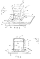
- Figure 1 is a perspective view of an applicator (with a portion cut away) and ground plate useful in the practice of the present invention.
- Figure 2 is a section view of the applicator and ground plate of Figure 1 taken along line 2-2 and including a continuous workload and supporting conveyor.
- Figure 3 shows greatly simplified views of the H fields at the walls of the cavity and E fields in a central plane of the cavity of the applicator of Figure 1.
- Figure 4 shows a top plan view of a greatly simplified view of the heating pattern produced by the applicator of Figure 1.
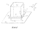
- Figure 5 is a perspective view of the applicator of Figures 1 and 2 of the present invention including greatly simplified views of currents in a corner region of the applicator and the cavity in phantom.
- Applicator 10 has a feed port or slot 12 fed by a conventional TE 10 waveguide 14. It is to be understood that this embodiment is intended for a predetermined frequency of operation of 2450 MHz with a magnetron 16 as the microwave source.
- the applicator 10 is made up of four sides 18, 20, 22, 24 and a top or roof 26.
- applicator 10 has a rectangular cross section with an interior "a" dimension 28 along an x-axis direction 34, an interior "b" dimension 32 along a y-axis direction 30, and an interior height or "h” dimension 36 along a z-axis direction 38.
- applicator 10 will have a square cross section when a and b dimensions 28 and 32 are equal.
- a horizontal metal plane or plate 40 is positioned in an x-y plane below the applicator 10 and a load 42 to be heated is carried by a support 44 which may include a moving belt of a microwave-transparent material 46.
- Applicator 10 has outwardly directed flanges 48 spaced a distance "h 0 " 50 from the metal plane 40.
- the load 42 may be a continuous strip of material, or a single piece, or a succession of discrete pieces.
- Load 42 is often a foodstuff, but the present invention is not limited to operation therewith, as other materials thermally responsive to the application of microwave energy may be irradiated by an embodiment of the present invention.
- the present invention is most suitable for use with load configurations having a low aspect ratio, i.e., a low or short load height (in the z direction) relative to the horizontal load dimensions (in the x and y directions).
- the distance 36 from the interior of the roof 26 to the plane of the flanges 48 plus the distance to the reflective surface parallel to and opposing the roof 26 will be the effective height, h e , of a cavity 78 of applicator 10.
- the effective height, h e is the sum of dimensions h 36 and h 1 37.
- the effective height of the cavity is more accurately approximated by the sum of the dimensions h 36 and h 0 50, extending from the interior of roof 26 to the surface of plate 40 facing the applicator 10.
- the difference may not be significant.
- the a dimension 28, b dimension 32, and the effective height h e (which is the sum of h dimension 36 and a distance between the h 0 dimension 50 and the h 1 dimension 37, depending upon the configuration of the load 42) and the type and position of the energy feed aperture 12 are selected for dominance of one hybrid mode.
- TM modes and hybrid modes sharing certain properties of TM modes are more favorable for heating purposes, since they can be more easily matched to the low impedance of typical loads, and therefore minimal reflections are built up. Using such modes avoids the necessity of careful and precise determination or adjustment of the cavity height and coupling factor to become efficient at resonance as is required with the use of TE modes.
- conditions for reflectionless transmission in at least a thick load that covers the whole horizontal cross section of the waveguide can be established.
- TE modes In a rectangular waveguide, except for the TE 0n and TE m0 modes, all TE modes have H fields in all directions and lack an E field in the direction of propagation, while all TM modes have E fields in all directions and lack an H field in the direction of propagation. It is evident from Equation (3) that some modes may have the same ⁇ ; these are called degenerate modes. They can be separated only by proper excitation, so that only one of the modes is excited. If the cross section is, for example, a regular square, mode degeneracies will, of course, be more common. The field patterns of degenerate modes can often be vectorially combined into simpler patterns of hybrid modes.
- the hybrid modes For rectangular waveguides with the z direction being that of propagation, one can then designate the hybrid modes as x- and y-directed, for example, TEx, TMy, TEz modes.
- TEx Time Warner Inc.
- TMy TMy
- TEz modes the subscript indicates the direction of the missing field component, i.e., for a TEx mode, Ex is missing; for a TMy mode, Hy is missing.
- a TEz mode the z directed component of the electric field is missing which makes it an ordinary TE mode.
- a hybrid mode with a z subscript is by definition an "ordinary" mode.
- (TEy) ⁇ g ( ⁇ o
- -(n ⁇ o /2b) 2 ] and (TEz) ⁇ g ⁇ o
- - ⁇ 2 where ⁇ 1 for empty space in the waveguide.
- a TEy 21 mode is a desired mode, giving maximum coupling to the load 42 if the effective cavity height, h e , is approximately p ⁇ g /2, where p is an integer.
- the mode should be (or behave similarly to) a TMz (TM) mode.
- the mode should also have a high normalized wavelength ⁇ , to obtain a low wave reflection at the upper surface 52 of the load 42 (for continuous or near continuous loads 42).
- n ⁇ 0 /2b is minimized, by making n small (preferably equal to 1), or by selecting a large "b" dimension 32, or both.
- the first is for drying relatively light loads or thawing frozen loads, each of which may be appropriately characterized by a dielectric constant having an absolute value of about 3.
- the second example is for compact, non-frozen loads where the dielectric constant is 9 or above.
- a dielectric constant having an absolute value of 10 provides an acceptable approximation for loads with higher dielectric constants.
- TM modes are used to calculate the Brewster condition. For a relatively low load permittivity,
- the guide wavelength is 245 mm for the first example and 392 mm for the second example, when each is calculated for a predetermined operating frequency of 2450 MHz.
- Equation (4) to give a favorably low value, (n ⁇ 0 /2b) 2 should be ⁇ 1.
- the (n ⁇ 0 /2b) 2 term becomes 0.15 for the larger embodiment and 0.18 for the smaller embodiment, each of which is acceptable.
- the larger embodiment relates to the low permittivity load and the smaller embodiment to the high permittivity load.
- a single embodiment having a side dimension of 151 mm can be used for loads with permittivity
- Equation (4) In order to obtain satisfactory matching of the microwave energy to the load, Equation (4) must be satisfied such that ⁇ from Equation (4) approximates ⁇ B from Equation (1). Since ⁇ 2 is to be made approximately equal to
- 10) ⁇ will equal 0.95 as the normalized wavelength. For the reasons stated previously, higher values for ⁇ are preferably avoided, and it has been found preferable to keep ⁇ equal to or less than about 0.95, as a compromise.
- h e has previously been defined for discrete and continuous loads.
- h e is preferably equal to about 123 mm or 246 mm.
- h e is preferably equal to about 196 mm or 392 mm. While this process results in a resonant condition for the desired mode, it is to be understood to be within the scope of the present invention to encompass designs which are non-resonant for the desired mode or modes, thus permitting an additional degree of freedom in making the longitudinal height anti-resonant for undesired modes, if desired.
- the height of the cavity is preferably sized to make undesired modes, particularly the TEy 11 mode, non-resonant.
- the guide wavelength is 146 mm in the larger applicator, and 153 mm in the smaller applicator.
- the desirable height is 255 mm.
- the height of 245 mm with the side dimension of 158 mm fulfills all the criteria for mode filtering of the undesired TEz 01 and TEz 02 modes while at the same time promoting or supporting the desired TEy 21 mode.
- the corresponding ⁇ g values are 135 and 232 mm for the undesired modes, while a height of 200 mm becomes resonant for the TEz 01 mode.
- the TEz 02 mode is not excited. Nevertheless, if the top surface of the load is controlled or limited to avoid a 200 mm effective height h e , the smaller applicator dimensions mentioned may also work well.
- the undesired TEz 01 , TEz 02 , and TEy 11 modes may also exist and be excited by the coupling slot 12 in the case where the slot is slightly asymmetrically positioned or the load is inhomogeneous in a way that reflections from it induce any of these modes.
- Data for these modes in the square applicator having sides of 158 mm, and the desired TEy 21 mode are given in Table 1.
- ⁇ g0 is the impedance in the air-filled portion of the waveguide or cavity
- ⁇ g ⁇ is the impedance in the dielectric filled portion (load) and the reflection factor is the fraction of power reflected from the load.
- the TEz 02 mode has a high impedance and becomes mismatched; its amplitude will become much less than that of the desired TEy 21 mode.
- the TEy 11 mode will not fulfill the conditions for resonance which are necessary for significant energy transfer to the load 42. As a result, the favorable low-impedance, well-matched and resonant TEy 21 mode will dominate. The influence of the TEy 11 mode can be tolerated as a slight imbalance between the strength of the major heating area lobes 56, 58, 60 illustrated in Figure 4.
- the index m can be 1, 2, 3, or larger. However, if m is larger than 3, the applicator may become too elongated both for practical integration in equipment and for reliable excitation by just one slot at a short wall.
- TEy 11 may, however, be a preferred or desired mode due to the larger physical dimensions at that frequency (where all dimensions are multiplied by the factor 2450/915).
- the desired TEy 21 hybrid mode pattern 70 is illustrated in Fig. 3. It is to be understood that although two rectilinear solids 78 are shown in Figure 3, each is a separate representation of the same volume: that of the cavity 78 of applicator 10. Furthermore, the field pattern 70 in the cavity 78 has H and E components existing simultaneously; the H field pattern 72 and the E field pattern 74 are separated only for clarity of illustration.
- the H field pattern 72 is a simplified view of the magnetic field component of the TEy 21 mode at the walls or sides 18-24 and top 26 of the cavity
- a narrow coupling slot as used herein provides a H field component along its major dimension, but only a perpendicular E field component. Since the H field lines are closed, the H field may have components in all directions some distance away from the slot in the interior or cavity of the applicator 10. However, the E field component is short circuited at the slot ends and must therefore be sinusoidal along the slot resulting in the absence of horizontal components of the E field along the major dimension of the slot. It has been found that in the practice of the present invention, a relatively long horizontal slot (about ⁇ 0 /2 or slightly longer) provides excitation of only the desired hybrid mode.
- a similar slot in the ceiling or roof of the applicator 10 also gives a horizontal x-directed E field component. There is still no y-directed component. (The E field lines still behave as indicated in Figure 3; the result becomes very similar for both slot positions).
- the main reason for preferring the slot in the side wall is that the mode wavelength along the short dimension of the slot is almost as short as possible when the slot is in the ceiling, whereas the mode wavelength is relatively long (typically >2 ⁇ 0 ) when the slot is placed in the side wall. Since the slot must have a physical size, it fits the field pattern better and disturbs the applicator pattern less if placed in the side wall close to the ceiling. In other words, the slot position is less sensitive (from a practical perspective) in the side wall than in the ceiling.
- the resulting hybrid mode components are favorable, since there is only a very weak E x and no external E y field near each y-directed edge of the load 42, thus eliminating edge overheating along these edges. Furthermore, the E z field is weakened by a factor between
- the direction of transport be aligned with the missing E field component to avoid edge overheating of the continuous side edges of the load.
- the effective height h e (between h+h 1 and h+h 0 ) is desirably ⁇ g /2, because resonant conditions are desirable for achieving the best possible impedance matching for variable
- the shortest height h e for this is about ⁇ g /z.
- the distance h is about 110 mm and the distance h 0 is about 35 mm for a 150x158 mm cross section applicator 10, with a thin, low permittivity load 42.
- the feeding waveguide 14 can conveniently be located at and affixed to a vertical applicator side, as at side wall 18 in Figures 1 and 2. Since the feed slot 12 is relatively small (typically 10x70 mm) and gives a well-defined field pattern as shown in Figure 3, the proper mode field is established at a relatively small distance away from the feed aperture 12.
- the leakage properties of the system can be assessed as follows, with reference to Fig. 5.
- Two types of fields exist at adjacent sides of the open end of the applicator 10. Taken together, the bottom edges of the four sides of the applicator 10 define an opening facing the plate 40 beneath the load 42.
- One type of field exists at the x-directed walls (that with the feeding slot, and the opposite wall) and another type of field exists at the y-directed walls. Referring first to the field at the x-directed walls, the applicator end is located so that h e ⁇ g /2 .
- the vertically directed H field becomes strongest at the corner 79, creating a strong horizontally directed wall current indicated by arrows 80.
- the continuity of the current will result in a strong current (indicated by arrows 82 in the horizontal flange 48 of applicator 10.
- This current is then linked to an outward-directed H field in the region just below the flange 48.
- the E field is very weak in this region, which means that the local field impedance is very low. Since the H field in this region is essentially parallel to the prospective direction of energy leakage (the unwanted Poynting vector direction), there are two reasons for low leakage: the H field direction and the low field impedance. In the central area of the vertical wall 18 near the flange 48 there will be no H field but some E field (y-directed).
- the other two applicator side regions or walls are in many respects similar to the x-directed side regions or walls.
- the horizontal y-directed H field strengths are only half of the corresponding x-directed below the x-directed walls due to the mode index relationship. This results in even less energy coupling out of the system in the region below the flanges 48 in the y-directed side regions than for the x-directed side regions.
- the applicator 10 with horizontal flanges 48 creates a low microwave leakage to the outside, so that a persistent field pattern in the load 42 is created and adjacent applicators will not interfere with another.
- the horizontal width 49 of the flanges 48 is determined by the requirement that the cutoff modes having outwardly directed E field components generally in the middle regions of the side walls be strongly damped. It is to be understood that the direction of propagation from this region is in the x and y directions, and that the simplest mode acting in this region is of the TM type. The properties of the TM 11 mode are of interest here for the opening between the flanges 48 and the ground plate 40.
- the power decay distance d d is defined to be the distance in the (local) direction of propagation where the power density has decayed to 1/e, where e is the Naperian base.
- 3d d 3d d
- a lossy load 42 may reduce the requirement for additional width in the flanges 48.
- adjacent applicators may share a common intermediate flange. It has been found that a 35 mm flange width is adequate for most applications, even with a low-loss load and a h 0 distance of 50 mm.
- Typical cross section dimensions for the TEy 31 mode are 155x230 mm, with the same height as for the other applicators described above.
- the applicator effective height (for any of the previously described TEy modes) is instead chosen to be about one vertical wavelength ⁇ g high, the filtering out of undesired modes may be enhanced.
- the non-symmetrical field pattern fulfilling the object of the invention can be compensated for by turning every second applicator in an array by an angle, e.g., 90°, around the vertical or longitudinal axis. Since the major heating pattern has three elongated areas in the y direction with an intensity which is essentially a sine squared function in this direction (see Fig. 4), more elaborate applicator-to-applicator orientations and displacements may be used for multi-applicator systems. In practice, a displacement equal to 1/3 of the side length a is in general satisfactory.
- two or even four magnetrons can be employed.
- One approach is to have two coupling slots, with one at each of two adjacent side walls. Since the hybrid modes become orthogonal, i.e., uncoupled, and the magnetrons do not oscillate coherently, the energy coupling between the magnetrons will become insignificant, provided the load is reasonably homogeneous and does not create any irregular current patterns.
- Another approach is to use magnetrons with power supplies fed in anti-phase (e.g., out-of-phase, non-overlapping half-wave supplies); their coupling slots may then be either at opposite or adjacent applicator walls, since a magnetron will not absorb power when not energized. Using both the methods described above enables the use of 4 magnetrons with the square cross section Tey 21 mode applicator.
- the multi-source executions just described may be preferable. If an allowed frequency in the band centered about 915 MHz is used, all dimensions given above are to be multiplied with 2450/915 ⁇ 2.68, and the side of the square cross section applicator dimension then becomes about 423 mm for the larger version of the preferred embodiment and 385 mm for the smaller example square applicator.
Landscapes
- Physics & Mathematics (AREA)
- Electromagnetism (AREA)
- Constitution Of High-Frequency Heating (AREA)
Claims (34)
- Rechtwinkliger Mikrowellenapplikator, der bei einer vorbestimmten Frequenz arbeitet und ein Mikrowellengehäuse umfaßt, das einen Hohlraum mit einer ersten und einer zweiten Querabmessung und einer Längsabmessung in Ausbreitungsrichtung der Mikrowellenenergie bildet, dadurch gekennzeichnet, daß jede der ersten und zweiten Querabmessungen so bemessen ist, um nur einen oder mehrere gewünschte Hybrid-Modi mit einer niedrigen Längsimpedanz und einem Fehlen einer transversalen E-Feld-Komponente in der ersten oder der zweiten Querrichtung aufrechtzuerhalten, so daß eine Last, die in dem Hohlraum in einem Bereich plaziert ist, der an einem stromabwärts befindlichen Ende des Gehäuses angrenzt, gleichmäßig ohne ein Überhitzen des Randes erwärmt wird.
- Applikator nach Anspruch 1, bei dem das Mikrowellengehäuse ein offenes Ende aufweist und der Applikator weiterhin eine metallische Erdungsplatte umfaßt, die von dem offenen Ende des Gehäuses mit Abstand angeordnet ist.
- Applikator nach Anspruch 2, bei dem das offene Ende des Applikators von Flanschen umgeben ist, die sich in die ersten und zweiten Querrichtungen mit einer Länge erstrecken, die ausreichend ist, um ein wesentliches Austreten der Mikrowellenenergie aus dem Gehäuse zu verhindern.
- Applikator nach Anspruch 1, bei dem das Gehäuse auf allen sechs Seiten geschlossen ist.
- Applikator nach Anspruch 1, bei dem die erste und zweite Querabmessung entsprechend den Gleichungen
- Applikator nach Anspruch 5, bei dem die Längsabmessung ausgewählt ist, um im wesentlichen Antiresonanzbedingungen für Modi vorzusehen, die in dem Hohlraum aufrechterhalten werden können und die eine darin vorhandene transversale E-Feld-Komponente aufweisen.
- Applikator nach Anspruch 1, bei dem der Hohlraum eine Zuführöffnung aufweist, die Mikrowellenenergie mit einer vorbestimmten Frequenz in den Hohlraum strahlt, wobei die Zuführöffnung eine im wesentlichen lange und schmale Apertur in einer Seitenwand des Applikators mit einer Längsabmessung der Apertur von ungefähr einer Hälfte der Raumwellenlänge der vorbestimmten Frequenz aufweist, so daß die Mikrowellenenergie, die in den Hohlraum durch die Zuführöffnung gestrahlt wird, nur jene Hybrid-Modi anregt, die keine horizontale E-Feld-Komponente in einer der Querrichtungen aufweist, um das Überhitzen des Randes einer Last zu vermeiden, der zu der einen Querrichtung ausgerichtet ist, die keine horizontale E-Feld-Komponente aufweist.
- Applikator nach Anspruch 1, bei dem die horizontale E-Feld-Komponente des hybriden Modus, der in der anderen Querrichtung angeregt wird, ausreichend schwach ist, um das Überhitzen des Randes einer Last zu vermeiden, der in der anderen Querrichtung ausgerichtet ist.
- Applikator nach Anspruch 1, bei dem die vorbestimmte Frequenz 2450 MHz und die erste Querabmessung ungefähr 151 bis ungefähr 165 mm beträgt, um einen TEy21-Modus in dem Hohlraum aufrechtzuerhalten, wenn die Dielektrizitätskonstante der Last ungefähr 3 beträgt.
- Applikator nach Anspruch 9, bei dem die zweite Querabmessung gleich der ersten Querabmessung ist.
- Applikator nach Anspruch 9, der eine Längsabmessung von ungefähr 120 bis ungefähr 140 mm aufweist.
- Applikator nach Anspruch 9, der weiterhin eine Längsabmessung von ungefähr 240 bis ungefähr 280 mm aufweist.
- Applikator nach Anspruch 1, bei dem die vorbestimmte Frequenz 2450 MHz und die erste Querabmessung ungefähr 137 bis ungefähr 151 mm betragen, um einen TEy21-Modus im Hohlraum aufrechtzuerhalten, wenn die Dielektrizitätskonstante der Last ungefähr 10 beträgt.
- Applikator nach Anspruch 1, bei dem die vorbestimmte Frequenz 2450 MHz und die erste Querabmessung ungefähr 151 mm betragen, um einen TEy21-Modus in dem Hohlraum aufrechtzuerhalten, wenn die Dielektrizitätskonstante der Last zwischen ungefähr 3 und ungefähr 10 liegt.
- Applikator nach Anspruch 1, bei dem die vorbestimmte Frequenz 915 MHz und die erste Querabmessung ungefähr 404 bis ungefähr 442 mm betragen, um einen TEy21-Modus im Hohlraum aufrechtzuerhalten, wenn die Dielektrizitätskonstante der Last ungefähr 3 beträgt.
- Applikator nach Anspruch 15, bei dem die zweite Querabmessung so ausgewählt ist, daß sie gleich der ersten Querabmessung ist.
- Applikator nach Anspruch 15, der eine Längsabmessung von ungefähr 321 bis ungefähr 375 mm aufweist.
- Applikator nach Anspruch 15, der eine Längsabmessung von ungefähr 643 bis ungefähr 752 mm aufweist.
- Applikator nach Anspruch 1, bei dem die vorbestimmte Frequenz 915 MHz und die erste Querabmessung ungefähr 367 bis ungefähr 404 mm betragen, um einen TEy21-Modus in dem Hohlraum aufrechtzuerhalten, wenn die Dielektrizitätskonstante der Last ungefähr 10 beträgt.
- Applikator nach Anspruch 1, bei dem die vorbestimmte Frequenz 915 MHz und die erste Querabmessung ungefähr 404 mm betragen, um einen TEy21-Modus in dem Hohlraum aufrechtzuerhalten, wenn die Dielektrizitätskonstante der Last zwischen ungefähr 3 und ungefähr 10 liegt.
- Applikator nach Anspruch 1, bei dem die effektive Längsabmessung des Hohlraums im wesentlichen gleich einem ganzzahligen Vielfachen der Hälfte der Leiterwellenlänge bei der vorbestimmten Frequenz für den gewünschten Hybrid-Modus ist.
- Applikator nach Anspruch 21, bei dem die effektive Längsabmessung des Hohlraums im wesentlichen gleich einem ungeraden ganzzahligen Vielfachen eines Viertels der Leiterwellenlänge bei der vorbestimmten Frequenz für zumindest einige unerwünschte Modi ist, die in dem Hohlraum neben den gewünschten Hybrid-Modi aufrechterhalten werden können, so daß für die unerwünschten Modi Antiresonanz erreicht wird.
- Applikator nach Anspruch 22, bei dem die Impedanz jedes unerwünschten Modus, der in dem Hohlraum aufrechterhalten werden kann, abgesehen von den unerwünschten Modi, für die Antiresonanz erreicht wurde, zur Lastimpedanz fehlangepaßt ist.
- Applikator nach Anspruch 23, bei dem das Verhältnis der Impedanz jedes unerwünschten Modus abgesehen von den einigen Modi, für die Antiresonanz erreicht wurde, zur Lastimpedanz größer als ungefähr 2 ist.
- Applikator nach Anspruch 1, der eine Transporteinrichtung zum Transportieren einer Last an dem offenen Ende des Applikators vorbei in einer der Querrichtungen umfaßt.
- Applikator nach Anspruch 25, bei dem die Transporteinrichtung einen Träger aus mikrowellendurchlässigem Material umfaßt.
- Applikator nach Anspruch 26, bei dem die fehlende E-Feld-Komponente in der ersten Querrichtung orientiert ist.
- Verfahren zum Bemessen eines Hohlraums für einen Mikrowellenapplikator, das die folgenden Schritte umfaßt:so daß durch das Fehlen einer E-Feld-Komponente in der einen Querrichtung das Überhitzen eines Randes der Last, der in dieser Querrichtung ausgerichtet ist, durch das Minimieren der E-Feld-Komponente in der zweiten Querrichtung im wesentlichen das Überhitzen eines Randes der Last, der zu der zweiten Querrichtung ausgerichtet ist, vermieden wird.a) Auswählen der Querabmessungen für einen Mikrowellenhohlraum, um nur einen oder mehrere gewünschte Hybrid-Modi, denen eine E-Feld-Komponente in einer ersten Querrichtung fehlt, aufrechtzuerhalten;b) Minimieren jeder E-Feld-Komponente in einer zweiten Querrichtung;c) Anordnen einer quergerichteten länglichen Apertur in einer Wand des Hohlraums, wobei die Apertur eine Längsabmessung im Bereich von dem ungefähr 0,9 bis 1,5-fachen der Raumwellenlänge der Mikrowellenfrequenz aufweist, um nur gewünschte Hybrid-Modi anzuregen, denen eine E-Feld-Komponente in der ersten Querrichtung fehlt; undd) Auswählen einer Längsabmessung in Richtung der Energieausbreitung in dem Hohlraum, um unerwünschte Modi zu einer Last fehlanzupassen und die gewünschten Hybrid-Modi, denen eine E-Feld-Komponente in der ersten Querrichtung fehlt, an die Last anzupassen, die so erwärmt werden soll, daß alle unerwünschten Modi entweder eine höhere Impedanz oder einen Antiresonanzzustand aufweisen, der sie von der Last entkoppelt,
- Verfahren nach Anspruch 28, das weiterhin die zusätzlichen Schritte umfaßt:e) Ausbilden des Applikators als ein Gehäuse mit einem offenen Ende, das eine Ebene definiert; undf) Positionieren einer Erdungsplatte entfernt von und parallel zu der Ebene des offenen Endes des Applikators, um die Dominanz des gewünschten Hybrid-Modus zu schaffen, dem eine transversale E-Feld-Komponente fehlt.
- Verfahren nach Anspruch 29, das weiterhin den zusätzlichen Schritt umfaßt:
g) Vorsehen eines Flansches an dem offenen Ende des Gehäuses, wobei sich der Flansch nach außen von dem Gehäuse in die Ebene des offenen Endes mit einer Länge erstreckt, die ausreichend ist, um die Grenz-Modi der Mikrowellenenergie, die in dem Bereich zwischen dem offenen Ende des Gehäuses und der Erdungsplatte vorhanden ist, so zu dämpfen, daß Mikrowellenenergie im wesentlichen daran gehindert wird, zwischen dem Flansch und der Erdungsebene zu entweichen. - Verfahren nach Anspruch 28, das weiterhin den zusätzlichen Schritt aufweist:
h) Vorsehen einer Transporteinrichtung zwischen dem offenen Ende des Gehäuses und der Erdungsebene, um eine Last an dem offenen Ende des Gehäuses in einer Ebene parallel zur Ebene des offenen Endes des Gehäuses vorbei zu transportieren. - Verfahren nach Anspruch 28, das die Schritte umfaßt:wobei die folgenden Schritte iterativ wiederholt werden:a) Auswählen einer gewünschten vorbestimmten Frequenz und Bestimmen, ob die Bearbeitungsfläche des Applikators über den praktischen Minimalgrenzen von etwa λ0/2 mal etwa 3λ0/4 liegt;b) Bestimmen einer normalisierten Wellenlänge νB für eine Last unter Verwendung von νB 2 = |ε|/(|ε|+1) mit einer Dielektrizitätskonstante ε für eine Last, die in den Applikator plaziert wird;c) Auswählen eines Wertes für den Modus-Index n;d) Bestimmen einer geeigneten Querabmessung "b" für einen Hohlraum des Applikators, indem der Ausdruck nλ0/2b so gesetzt wird, daß er weniger als ungefähr ½ beträgt;e) Bestimmen einer geeigneten Kombination der Querabmessung "a" für den Hohlraum und einem ganzahligen Modus-Index m, der die allgemeinen Größenkriterien für den Applikator erfüllt, unter Verwendung von ν2 =(λ0)2 [(m/2a)2 + (n/2b)2] mit den Werten von ν, λ0, n und b, wie sie vorab bestimmt wurden (unter anfänglicher Verwendung des Wertes νB für ν);f) Bestimmen eines Wertes von v unter Verwendung von ν2 =(λ0)2 [(m/2a)2 + (n/2b)2] mit den Werten von λ0, m, n, "a" und "b" aus Schritt c);g) Überprüfen der Abmessungsgenauigkeit, indem das Ergebnis des Schritts f) getestet wird, um zu bestimmen, ob ν > 0,95 ist; und wenn ja, Zurückkehren zu den Schritten c), d) und e) und Auswählen einer neuen Wertemenge für zumindest einige der Werte n, m, "a" und "b";h) Bestimmen der Impedanz, ηg0, für einen interessierenden Modus mit ηg0 = (η0i) Bestimmen der Impedanz der Last ηgε unter Verwendung der Dielektrizitätskonstanten der Last aus Schritt b) in der Gleichung ηgε = (η0j) Bestimmen des Quotienten von ηg0/ηgε für den interessierenden Modus;k) Überprüfen der Impedanz-Übereinstimmung, die im Schritt j) berechnet wurde und wenn das Ergebnis größer als 3 ist, Zurückkehren zu den Schritten c), d) und e) und Auswählen einer neuen Wertemenge für zumindest einige Werte n, "a", "b" und m;l) Berechnen der v-Werte aller unerwünschten TEz, TMz und TEy- Modi mit gleichen oder geringeren Modus-Indices unter Verwendung von ν2 = (λ0)2 [(m/2a)2 + (n/2b)2] mit den vorab bestimmten Abmessungen "a" und "b";m) Bestimmen der Leiterwellenlänge λg = λ0/n) wenn der Quotient aus Schritt j) zwischen 1 und ungefähr 2 liegt, Auswählen einer Höhe für den Hohlraum einschließlich eines Abstandes zur Last von ungefähr pλg0/2, wobei p für den gewünschten Modus ganzzahlig ist;o) Teilen der Höhe, die zuletzt in Schritt n) bestimmt wurde, durch die Hälfte der Leiterwellenlänge λg0 auf mindestens zwei Dezimalstellen genau für alle möglichen unerwünschten Modi; undp) Prüfen des Ergebnisses des Schrittes o), um festzustellen, ob das Ergebnis innerhalb 10% einer ganzen Zahl für jeden unerwünschten Modus ist, und wenn ja, Verwerfen der ausgewählten Abmessungen und Wiederholen der Schritte n), o) und p), Ändern der Höhe direkt oder durch Hinzuzählen des ganzzahligen p und falls ein akzeptierbares Ergebnis, das alle Prüfungen erfüllt, nicht erreicht wird, Wiederholen der Schritte e) bis o), wobei zunächst die Abmessungen "a" und Index m geändert werden und falls dies zu keinem akzeptierbaren Ergebnis führt, Wiederholen der Schritte d) bis o) mit einer neuen Abmessung "b" und notwendigenfalls Verändern des Index n auf einen weiteren ganzzahligen Wert und Rückkehr zum Schritt c), bis alle Prüfungen erfüllt werden, und Fortfahren zu Schritt q), wenn ein oder mehrere unerwünschte Modi die Prüfung dieses Schrittes p) durch Anpassen der Höhe nicht erfüllen können;q) Bestimmen sowohl der ηg0 Impedanz der TMz-Modi, die in Schritt 1) unter Verwendung von ηg = (η0r) Testen des Quotienten ηg0/ηgε für jene Werte von ηg0 die in Schritt p) bestimmt wurden, um festzustellen, ob der Quotient größer als 2 ist und wenn nicht, Wiederholen der Schritte c) bis r) bis der Quotient größer als 2 ist; und nachfolgend, nachdem alle Prüfungen erfüllt worden sind,s) Bauen eines Mikrowellenapplikators aus mikrowellenreflektierendem mit zwei Querabmessungen "a" und "b", die oben bestimmt wurden, so daß bei der vorbestimmten Frequenz der Hohlraum einen gewünschten Hybrid-Modus, dem eine transversale E-Feld-Komponente fehlt, und eine niedrige Wellenimpedanz in der Längsrichtung aufweist, die im wesentlichen mit derjenigen einer Last übereinstimmt, die durch den Applikator bestrahlt werden soll, und bei dem alle unerwünschten Modi, die in dem Hohlraum aufrechterhalten werden können, entweder eine hohe Längsimpedanz aufweisen oder sich in dem Hohlraum in einem Antiresonanzzustand befinden.
- Applikator nach Anspruch 1, bei dembei dem das Gehäuse und die Erdungsplatte den Hohlraum bilden, der den einen oder die mehreren gewünschten Hybrid-Modi enthält, die eine niedrige Wellenimpedanz in der Längsrichtung und ein Fehlen einer E-Feld-Komponente in zumindestens einer der Querrichtungen aufweisen, und die alle durch die Querabmessungen des Hohlraums und durch eine vorbestimmte, in dem Hohlraum befindliche Mikrowellenfrequenz bestimmt sind.a) das Gehäuse aus mikrowellenreflektierendem Material besteht und ein geschlossenes erstes Ende, vier Seitenwände und ein offenes zweites Ende aufweist und der weiterhin umfaßt:b) eine Erdungsplatte, die von dem offenen Ende des Gehäuses mit Abstand angeordnet ist und diesem gegenüber liegt, wobei sich die Erdungsplatte in zwei Querrichtungen erstreckt und rechtwinklig dazu eine Längsrichtung aufweist,
- Applikator nach Anspruch 1, bei dem das Gehäuse aus mikrowellenreflektierendem Material mit sechs geschlossenen Wänden gebildet ist, die den Hohlraum bilden.
Applications Claiming Priority (2)
| Application Number | Priority Date | Filing Date | Title |
|---|---|---|---|
| US455114 | 1995-05-31 | ||
| US08/455,114 US5828040A (en) | 1995-05-31 | 1995-05-31 | Rectangular microwave heating applicator with hybrid modes |
Publications (3)
| Publication Number | Publication Date |
|---|---|
| EP0746182A2 EP0746182A2 (de) | 1996-12-04 |
| EP0746182A3 EP0746182A3 (de) | 1997-05-28 |
| EP0746182B1 true EP0746182B1 (de) | 2000-08-09 |
Family
ID=23807462
Family Applications (1)
| Application Number | Title | Priority Date | Filing Date |
|---|---|---|---|
| EP96108790A Expired - Lifetime EP0746182B1 (de) | 1995-05-31 | 1996-05-31 | Rechteckiger Mikrowellenapplikator |
Country Status (6)
| Country | Link |
|---|---|
| US (1) | US5828040A (de) |
| EP (1) | EP0746182B1 (de) |
| CA (1) | CA2177905A1 (de) |
| DE (1) | DE69609671T2 (de) |
| DK (1) | DK0746182T3 (de) |
| ES (1) | ES2150048T3 (de) |
Families Citing this family (15)
| Publication number | Priority date | Publication date | Assignee | Title |
|---|---|---|---|---|
| FR2751055B1 (fr) * | 1996-07-15 | 1998-09-25 | Moulinex Sa | Four electrique de cuisson |
| SE512162C2 (sv) * | 1998-03-16 | 2000-02-07 | Rubbright Group Inc | Mikrovågsvärmningsapparat |
| US6444964B1 (en) * | 2000-05-25 | 2002-09-03 | Encad, Inc. | Microwave applicator for drying sheet material |
| SE0201755D0 (sv) * | 2002-06-07 | 2002-06-07 | O Risman | Improvements of hybrid mode rectangular heating applicators |
| SE526169C2 (sv) * | 2003-09-02 | 2005-07-19 | Exh Llc | Mikrovågsvärmningsapplikator |
| AU2006325574A1 (en) * | 2005-12-13 | 2007-06-21 | Exh Llc | Microwave heating applicator |
| CN103384421B (zh) | 2006-02-21 | 2016-09-28 | 高知有限公司 | 电磁加热 |
| US10674570B2 (en) | 2006-02-21 | 2020-06-02 | Goji Limited | System and method for applying electromagnetic energy |
| US8653482B2 (en) | 2006-02-21 | 2014-02-18 | Goji Limited | RF controlled freezing |
| US8839527B2 (en) | 2006-02-21 | 2014-09-23 | Goji Limited | Drying apparatus and methods and accessories for use therewith |
| US9131543B2 (en) | 2007-08-30 | 2015-09-08 | Goji Limited | Dynamic impedance matching in RF resonator cavity |
| ES2394919T3 (es) | 2008-11-10 | 2013-02-06 | Goji Limited | Dispositivo y método para controlar energía |
| ES2534411T3 (es) | 2009-11-10 | 2015-04-22 | Goji Limited | Dispositivo y método para el control de la energía |
| WO2011138688A2 (en) | 2010-05-03 | 2011-11-10 | Goji Ltd. | Loss profile analysis |
| PL2445312T3 (pl) * | 2010-10-22 | 2017-06-30 | Whirlpool Corporation | Mikrofalowe urządzenie podgrzewające i sposób działania takiego mikrofalowego urządzenia podgrzewającego |
Family Cites Families (12)
| Publication number | Priority date | Publication date | Assignee | Title |
|---|---|---|---|---|
| US2500752A (en) * | 1946-06-01 | 1950-03-14 | Gen Electric | High-frequency dielectric heating in a resonant chamber |
| GB977777A (en) * | 1962-02-02 | 1964-12-16 | Lyons & Co Ltd J | Improvements in or relating to radio frequency ovens |
| US3177333A (en) * | 1962-08-02 | 1965-04-06 | Tappan Co | Conveyor microwave oven |
| DE1924523A1 (de) * | 1969-05-14 | 1970-11-19 | Fritz Dr Karl | Hochfrequenzherd II |
| FR2128935A5 (de) * | 1971-03-09 | 1972-10-27 | Thomson Csf | |
| US3764770A (en) * | 1972-05-03 | 1973-10-09 | Sage Laboratories | Microwave oven |
| US3855440A (en) * | 1974-01-04 | 1974-12-17 | Gen Electric | Microwave oven having preferred modes |
| US3845267A (en) * | 1974-01-04 | 1974-10-29 | Gen Electric | Microwave oven with waveguide feed |
| US3961152A (en) * | 1974-01-04 | 1976-06-01 | General Electric Company | Magnetron power supply and control circuit |
| US3843862A (en) * | 1974-01-04 | 1974-10-22 | Gen Electric | Microwave oven having tm and te modes |
| DE3120900A1 (de) * | 1981-05-26 | 1983-06-16 | Karl Dr. 7800 Freiburg Fritz | Mikrowellen-arbeitsraum |
| FR2660147A1 (fr) * | 1990-03-20 | 1991-09-27 | Transitube Sa | Installation pour proceder en continu au sechage, a la deshydratation ou a la cuisson par micro-ondes de produits granuleux ou pulverulents. |
-
1995
- 1995-05-31 US US08/455,114 patent/US5828040A/en not_active Expired - Fee Related
-
1996
- 1996-05-31 ES ES96108790T patent/ES2150048T3/es not_active Expired - Lifetime
- 1996-05-31 DK DK96108790T patent/DK0746182T3/da active
- 1996-05-31 DE DE69609671T patent/DE69609671T2/de not_active Expired - Fee Related
- 1996-05-31 EP EP96108790A patent/EP0746182B1/de not_active Expired - Lifetime
- 1996-05-31 CA CA002177905A patent/CA2177905A1/en not_active Abandoned
Also Published As
| Publication number | Publication date |
|---|---|
| ES2150048T3 (es) | 2000-11-16 |
| DE69609671D1 (de) | 2000-09-14 |
| DE69609671T2 (de) | 2001-04-12 |
| CA2177905A1 (en) | 1996-12-01 |
| DK0746182T3 (da) | 2000-12-27 |
| US5828040A (en) | 1998-10-27 |
| EP0746182A3 (de) | 1997-05-28 |
| EP0746182A2 (de) | 1996-12-04 |
Similar Documents
| Publication | Publication Date | Title |
|---|---|---|
| EP0746182B1 (de) | Rechteckiger Mikrowellenapplikator | |
| EP1013150B1 (de) | Rohrförmige mikrowellenapplikator | |
| US4165454A (en) | Microwave oven | |
| US4354083A (en) | Microwave oven with novel energy distribution arrangement | |
| US7230218B2 (en) | Microwave or radio frequency device including three decoupled generators | |
| AU2004302755B2 (en) | Microwave heating applicator | |
| US8324539B2 (en) | Wide waveguide applicator | |
| US6072167A (en) | Enhanced uniformity in a length independent microwave applicator | |
| US7528353B2 (en) | Microwave heating device | |
| CN111183708B (zh) | 微波处理装置 | |
| JPS58176896A (ja) | マイクロ波加熱装置 | |
| WO2001022783A2 (en) | Apparatus and method for generating ultraviolet radiation | |
| WO2000024228A1 (en) | Microwave apparatus and method for heating thin loads | |
| US20090166354A1 (en) | Microwave Heating Applicator | |
| JPH08330065A (ja) | マイクロ波解凍加熱装置 | |
| JP3269683B2 (ja) | 漏れ波nrdガイド | |
| JP2000150137A5 (de) | ||
| JPS59101791A (ja) | 高周波加熱装置 | |
| JP2000150137A (ja) | マイクロ波加熱装置 | |
| JPH08138857A (ja) | 高周波加熱装置 | |
| JPH1154256A (ja) | マイクロ波加熱装置 |
Legal Events
| Date | Code | Title | Description |
|---|---|---|---|
| PUAI | Public reference made under article 153(3) epc to a published international application that has entered the european phase |
Free format text: ORIGINAL CODE: 0009012 |
|
| AK | Designated contracting states |
Kind code of ref document: A2 Designated state(s): DE DK ES FR GB IT NL SE |
|
| PUAL | Search report despatched |
Free format text: ORIGINAL CODE: 0009013 |
|
| AK | Designated contracting states |
Kind code of ref document: A3 Designated state(s): DE DK ES FR GB IT NL SE |
|
| 17P | Request for examination filed |
Effective date: 19970814 |
|
| 17Q | First examination report despatched |
Effective date: 19990208 |
|
| GRAG | Despatch of communication of intention to grant |
Free format text: ORIGINAL CODE: EPIDOS AGRA |
|
| GRAG | Despatch of communication of intention to grant |
Free format text: ORIGINAL CODE: EPIDOS AGRA |
|
| GRAH | Despatch of communication of intention to grant a patent |
Free format text: ORIGINAL CODE: EPIDOS IGRA |
|
| GRAH | Despatch of communication of intention to grant a patent |
Free format text: ORIGINAL CODE: EPIDOS IGRA |
|
| GRAA | (expected) grant |
Free format text: ORIGINAL CODE: 0009210 |
|
| AK | Designated contracting states |
Kind code of ref document: B1 Designated state(s): DE DK ES FR GB IT NL SE |
|
| REF | Corresponds to: |
Ref document number: 69609671 Country of ref document: DE Date of ref document: 20000914 |
|
| ITF | It: translation for a ep patent filed | ||
| REG | Reference to a national code |
Ref country code: ES Ref legal event code: FG2A Ref document number: 2150048 Country of ref document: ES Kind code of ref document: T3 |
|
| ET | Fr: translation filed | ||
| REG | Reference to a national code |
Ref country code: DK Ref legal event code: T3 |
|
| PLBE | No opposition filed within time limit |
Free format text: ORIGINAL CODE: 0009261 |
|
| STAA | Information on the status of an ep patent application or granted ep patent |
Free format text: STATUS: NO OPPOSITION FILED WITHIN TIME LIMIT |
|
| 26N | No opposition filed | ||
| REG | Reference to a national code |
Ref country code: GB Ref legal event code: IF02 |
|
| PGFP | Annual fee paid to national office [announced via postgrant information from national office to epo] |
Ref country code: SE Payment date: 20020508 Year of fee payment: 7 Ref country code: FR Payment date: 20020508 Year of fee payment: 7 |
|
| PGFP | Annual fee paid to national office [announced via postgrant information from national office to epo] |
Ref country code: DK Payment date: 20020514 Year of fee payment: 7 |
|
| PGFP | Annual fee paid to national office [announced via postgrant information from national office to epo] |
Ref country code: ES Payment date: 20020522 Year of fee payment: 7 |
|
| PGFP | Annual fee paid to national office [announced via postgrant information from national office to epo] |
Ref country code: NL Payment date: 20020529 Year of fee payment: 7 Ref country code: GB Payment date: 20020529 Year of fee payment: 7 |
|
| PGFP | Annual fee paid to national office [announced via postgrant information from national office to epo] |
Ref country code: DE Payment date: 20020610 Year of fee payment: 7 |
|
| PG25 | Lapsed in a contracting state [announced via postgrant information from national office to epo] |
Ref country code: GB Free format text: LAPSE BECAUSE OF NON-PAYMENT OF DUE FEES Effective date: 20030531 |
|
| PG25 | Lapsed in a contracting state [announced via postgrant information from national office to epo] |
Ref country code: SE Free format text: LAPSE BECAUSE OF NON-PAYMENT OF DUE FEES Effective date: 20030601 |
|
| PG25 | Lapsed in a contracting state [announced via postgrant information from national office to epo] |
Ref country code: ES Free format text: LAPSE BECAUSE OF NON-PAYMENT OF DUE FEES Effective date: 20030602 |
|
| PG25 | Lapsed in a contracting state [announced via postgrant information from national office to epo] |
Ref country code: NL Free format text: LAPSE BECAUSE OF NON-PAYMENT OF DUE FEES Effective date: 20031201 Ref country code: DK Free format text: LAPSE BECAUSE OF NON-PAYMENT OF DUE FEES Effective date: 20031201 |
|
| PG25 | Lapsed in a contracting state [announced via postgrant information from national office to epo] |
Ref country code: DE Free format text: LAPSE BECAUSE OF NON-PAYMENT OF DUE FEES Effective date: 20031202 |
|
| REG | Reference to a national code |
Ref country code: DK Ref legal event code: EBP |
|
| GBPC | Gb: european patent ceased through non-payment of renewal fee |
Effective date: 20030531 |
|
| PG25 | Lapsed in a contracting state [announced via postgrant information from national office to epo] |
Ref country code: FR Free format text: LAPSE BECAUSE OF NON-PAYMENT OF DUE FEES Effective date: 20040130 |
|
| NLV4 | Nl: lapsed or anulled due to non-payment of the annual fee |
Effective date: 20031201 |
|
| EUG | Se: european patent has lapsed | ||
| REG | Reference to a national code |
Ref country code: FR Ref legal event code: ST |
|
| REG | Reference to a national code |
Ref country code: ES Ref legal event code: FD2A Effective date: 20030602 |
|
| PG25 | Lapsed in a contracting state [announced via postgrant information from national office to epo] |
Ref country code: IT Free format text: LAPSE BECAUSE OF NON-PAYMENT OF DUE FEES;WARNING: LAPSES OF ITALIAN PATENTS WITH EFFECTIVE DATE BEFORE 2007 MAY HAVE OCCURRED AT ANY TIME BEFORE 2007. THE CORRECT EFFECTIVE DATE MAY BE DIFFERENT FROM THE ONE RECORDED. Effective date: 20050531 |