EP0746144A2 - CCD type solid state image pickup device - Google Patents
CCD type solid state image pickup device Download PDFInfo
- Publication number
- EP0746144A2 EP0746144A2 EP96108795A EP96108795A EP0746144A2 EP 0746144 A2 EP0746144 A2 EP 0746144A2 EP 96108795 A EP96108795 A EP 96108795A EP 96108795 A EP96108795 A EP 96108795A EP 0746144 A2 EP0746144 A2 EP 0746144A2
- Authority
- EP
- European Patent Office
- Prior art keywords
- vertical shift
- output register
- photo
- horizontal output
- signal charges
- Prior art date
- Legal status (The legal status is an assumption and is not a legal conclusion. Google has not performed a legal analysis and makes no representation as to the accuracy of the status listed.)
- Withdrawn
Links
- 239000007787 solid Substances 0.000 title claims abstract description 15
- 238000006243 chemical reaction Methods 0.000 claims abstract description 38
- 238000010586 diagram Methods 0.000 description 12
- 230000005684 electric field Effects 0.000 description 4
- XAGFODPZIPBFFR-UHFFFAOYSA-N aluminium Chemical compound [Al] XAGFODPZIPBFFR-UHFFFAOYSA-N 0.000 description 3
- 229910052782 aluminium Inorganic materials 0.000 description 3
- 238000009792 diffusion process Methods 0.000 description 2
- 239000012535 impurity Substances 0.000 description 2
- 238000000034 method Methods 0.000 description 2
- 229910021420 polycrystalline silicon Inorganic materials 0.000 description 2
- 244000118350 Andrographis paniculata Species 0.000 description 1
- 239000004065 semiconductor Substances 0.000 description 1
- 239000000758 substrate Substances 0.000 description 1
Images


Classifications
-
- H—ELECTRICITY
- H01—ELECTRIC ELEMENTS
- H01L—SEMICONDUCTOR DEVICES NOT COVERED BY CLASS H10
- H01L27/00—Devices consisting of a plurality of semiconductor or other solid-state components formed in or on a common substrate
- H01L27/14—Devices consisting of a plurality of semiconductor or other solid-state components formed in or on a common substrate including semiconductor components sensitive to infrared radiation, light, electromagnetic radiation of shorter wavelength or corpuscular radiation and specially adapted either for the conversion of the energy of such radiation into electrical energy or for the control of electrical energy by such radiation
- H01L27/144—Devices controlled by radiation
- H01L27/146—Imager structures
- H01L27/148—Charge coupled imagers
-
- H—ELECTRICITY
- H04—ELECTRIC COMMUNICATION TECHNIQUE
- H04N—PICTORIAL COMMUNICATION, e.g. TELEVISION
- H04N25/00—Circuitry of solid-state image sensors [SSIS]; Control thereof
- H04N25/70—SSIS architectures; Circuits associated therewith
- H04N25/71—Charge-coupled device [CCD] sensors; Charge-transfer registers specially adapted for CCD sensors
- H04N25/73—Charge-coupled device [CCD] sensors; Charge-transfer registers specially adapted for CCD sensors using interline transfer [IT]
Definitions
- the present invention relates to a charge coupled device (CCD)type solid state image pickup device.
- CCD charge coupled device
- a prior art CCD type solid state image pickup device includes two-dimensionally arranged photo/electro conversion portions, a plurality of vertical shift registers each connected to one column of the photo/electro conversion portions, and a horizontal output register connected to the vertical shift registers, signal charges of every two of each column of the photo/electro conversion portions are mixed within the vertical shift registers, to creat a mixed signal charge. Then, the mixed signal charge corresponding to two of the photo/electro conversion portions is transferred within the horizontal output register. Thus, one scanning line is formed by every two rows of the photo/electro conversion portions. This will be explained later in detail.
- a CCD type solid state image pickup device including two-dimensionally arranged photo/electro conversion portions, a plurality of vertical shift registers each connected to one column of the photo/electro conversion portions, and a horizontal output register connected to the vertical shift registers
- signal charges of every four of each column of the photo/electro conversion portions are mixed within the vertical shift registers or within the vertical shift registers and the horizontal output register, to create a mixed signal charge.
- the mixed signal charge corresponding to four of the photo/electro conversion portions is transferred within the horizontal output register.
- one scanning line is formed by every four rows of the photo/electro conversion portions. This increases the ratio of a width to a length of transfer electrodes of the vertical shift registers.
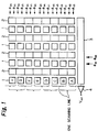
- Fig. 1 is a plan view illustrating a prior art CCD type solid state image pickup device
- light is incident to two-dimensionally arranged photo/electro conversion portions 1 formed by photo diodes, and as a result, signal charges obtained by the photo/electro conversion portions 1 are transferred to vertical shift registers 2.
- the signal charges are further transferred via a horizontal output register 3 to a signal charge output register 4 which generates an output voltage V out .
- the vertical shift registers 2 are operated by four-phase transfer pulse signals ⁇ V1 , ⁇ V2 , ⁇ V3 and ⁇ V4
- the horizontal output register 3 is operated by two-phase transfer pulse signals ⁇ H1 and ⁇ H2 .
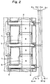
- each of the photo/electro conversion portions 1 includes a P + -type impurity diffusion region and an N-type impurity diffusion region formed on a P-type well region of a N-type semiconductor substrate.
- the vertical shift registers 2 include N-type buried channels formed on the P-type well region.
- read gate regions 5 Provided between the photo/electro conversion portions 1 and the vertical shift registers 2 are read gate regions 5. Every column of the photo/electro portions 1 and the vertical shift registers 2 are isolated from the other columns by a P + -type channel stopper region 6.
- the transfer electrodes 8 and 9 are provided for each column of the photo/electro conversion portions 1.
- the transfer electrodes 8 also serve as read gates for the read gate regions 5.
- the transfer electrodes 9 are made of a first polycrystalline silicon layer, and the transfer electrodes 8 are made of a second polycrystalline silicon layer.
- bus lines 10-1, 10-2, 10-3 and 10-4 made of aluminum are provided and connected to the transfer electrodes 8 and 9.
- the transfer pulse signals ⁇ V1 , ⁇ V2 , ⁇ V3 and ⁇ V4 are supplied to the bus lines 10-1, 10-2, 10-3 and 10-4, respectively.
- the operation of the device of Fig. 1 is interlaced scanning.
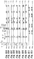
- the transfer pulse signals ⁇ V1 , ⁇ V2 , ⁇ V3 and ⁇ V4 are V L , V M , V H and V L , respectively, as shown in Figs. 3A, 3B, 3C and 3D.
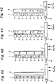
- the signal charges Q A , Q C , Q E and Q G are read out to the vertical shift register 2 as shown in Fig. 4B.
- the transfer pulse signals ⁇ V1 , ⁇ V2 , ⁇ V3 and ⁇ V4 are V H , V L , V L and V M , respectively, as shown in Figs. 3A, 3B, 3C and 3D.
- the signal charges Q E , Q D , Q F and Q H are read out to the vertical shift register 2 as shown in Fig. 4C.
- the charges Q B , Q D , Q F and Q H are added to the charges Q A , Q C , Q E and Q G , respectively, to form signal charges Q A + Q B , Q C + Q D , Q E + Q F and Q G + Q H .
- the transfer pulse signals ⁇ V1 , ⁇ V2 , ⁇ V3 and ⁇ V4 are V M , V M , V M and V L , respectively, as shown in Figs. 3A, 3B, 3C and 3D, and as a result, the potential wells are deep as shaded at time t1 in Fig. 5.
- the transfer pulse signals ⁇ V1 , ⁇ V2 , ⁇ V3 and ⁇ V4 are V L , V M , V M and V L , respectively, as shown in Figs. 3A, 3B, 3C and 3D, and as a result, the potential wells are deep as shaded at time t2 in Fig. 5.
- the transfer pulse signals ⁇ V1 , ⁇ V2 , ⁇ V3 and ⁇ V4 are V L , V L , V M and V M , respectively, as shown in Figs. 3A, 3B, 3C and 3D, and as a result, the potential wells are deep as shaded at time t3 in Fig. 5.
- the transfer pulse signals ⁇ V1 , ⁇ V2 , ⁇ V3 and ⁇ V4 are V M , V L , V L and V M , respectively, as shown in Figs.
- the transfer pulse signals ⁇ V1 , ⁇ V2 , ⁇ V3 and ⁇ V4 are V M , V M , V L and V L , respectively, as shown in Figs. 3A, 3B, 3C and 3D, and as a result, the potential wells are deep as shaded at time t5 in Fig. 5.
- the transfer pulse signals ⁇ V1 , ⁇ V2 , ⁇ V3 and ⁇ V4 are V L , V M , V M and V L , respectively, as shown in Figs. 3A, 3B, 3C and 3D, and as a result, the potential wells are deep as shaded at time t6 in Fig. 5.
- the vertical shift register 2 carries out a one-pixel vertical shift operation, so that the signal charge Q A + Q B is transferred to the horizontal output register 3 as shown in Fig. 4D.
- the transfer pulse signals ⁇ V1 , ⁇ V2 , ⁇ V3 and ⁇ V4 are changed at times t7, t8, t9 and t10 in the same way as at times t3, t4, t5 and t6 as shown in Figs. 3A, 3B, 3C and 3D.
- the vertical shift register 2 carries out another one-pixel vertical shift operation, so that the signal charge Q C + Q D is transferred to the horizontal output register 3.
- the transfer pulse signals ⁇ H1 and ⁇ H2 are changed as shown in Figs. 3E and 3F, so that the horizontal output register 3 performs a one-horizontal line shift operation upon the signal charge Q C + Q D and the like.
- the transfer pulse signals ⁇ V1 , ⁇ V2 , ⁇ V3 and ⁇ V4 are V L , V M , V H and V L , respectively, as shown in Figs. 6A, 6B, 6C and 6D.
- the signal charges Q A , Q C , Q E and Q G arde read out to the vertical shift register 2 as shown in Fig. 7B.
- the transfer pulse signals ⁇ V1 , ⁇ V2 , ⁇ V3 and ⁇ V4 are V H , V L , V L and V M , respectively, as shown in Figs. 6A, 6B, 6C and 6D.
- the signal charges Q B , Q D , Q F and Q H arde read out to the vertical shift register 2 as shown in Fig.4C.
- the charges Q B , Q D and Q F are added to the charges Q C , Q E and Q G , respectively, to form signal charges Q B + Q C , Q D + Q E and Q F + Q G .
- the transfer pulse signals ⁇ V1 , ⁇ V2 , ⁇ V3 and ⁇ V4 are V M , V M , V M and V L , respectively, as shown in Figs. 6A, 6B, 6C and 6D, and as a result, the potential wells are deep as shaded at time t1 in Fig. 8.
- the transfer pulse signals ⁇ V1 , ⁇ V2 , ⁇ V3 and ⁇ V4 are V L , V M , V M and V L , respectively, as shown in Figs. 6A, 6B, 6C and 6D, and as a result, the potential wells are deep as shaded at time t2 in Fig. 8.
- the transfer pulse signals ⁇ V1 , ⁇ V2 , ⁇ V3 and ⁇ V4 are V L , V L , V M and V M , respectively, as shown in Figs. 6A, 6B, 6C and 6D, and as a result, the potential wells are deep as shaded at time t3 in Fig. 8.
- the transfer pulse signals ⁇ V1 , ⁇ V2 , ⁇ V3 and ⁇ V4 are V M , V L , V L and V M , respectively, as shown in Figs.
- the transfer-pulse signals ⁇ V1 , ⁇ V2 , ⁇ V3 and ⁇ V4 are V M , V M , V L and V L , respectively, as shown in Figs. 6A, 6B, 6C and 6D, and as a result, the potential wells are deep as shaded at time t5 in Fig. 8A.
- the transfer pulse signals ⁇ V1 , ⁇ V2 , ⁇ V3 and ⁇ V4 are V L , V M , V M and V L , respectively, as shown in Figs. 6A, 6B, 6C and 6D, and as a result, the potential wells are deep as shaded at time t6 in Fig. 8A.
- the vertical shift register 2 carries out a one-pixel vertical shift operation, so that the signal charge Q A is transferred to the horizontal output register 3 as shown in Fig. 7D.
- the transfer pulse signals ⁇ V1 , ⁇ V2 , ⁇ V3 and ⁇ V4 are changed at times t7, t8, t9 and t10 in the same way as at times t3, t4, t5 and t6 as shown in Figs. 6A, 6B, 6C and 6D.
- the vertical shift register 2 carries out another one-pixel vertical shift operation, so that the signal charge Q B + Q C is transferred to the horizontal output register 3 as shown in Fig. 7E.
- the transfer pulse signals ⁇ H1 and ⁇ H2 are changed as shown in Figs. 6E and 6F, so that the horizontal output register 3 performs a one-horizontal line shift operation upon the signal charge Q B + Q C and the like.
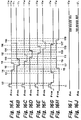
- Fig. 8B which illustrates a first embodiment of the present invention
- every four of the photo/electro conversion portions 1 form one scanning line.
- the vertical shift registers 2 may be operated by eight-phase transfer pulse signals; however, the vertical shift registers 2 are operated by six-phase transfer pulse signals ⁇ V1A , ⁇ V2 , ⁇ V3A , ⁇ V4 , ⁇ V1B and ⁇ V3B . Therefore, as illustrated in Fig. 9, six bus lines 10-1, 10-2, 10-3, 10-4, 10-5 and 10-6 made of aluminum are provided and connected to the transfer electrodes 8 and 9.
- the transfer pulse signals ⁇ V1A , ⁇ V2 , ⁇ V3A , ⁇ V4 , ⁇ V1B and ⁇ V3B are supplied to the bus lines 10-1, 10-2, 10-3, 10-4, 10-5 and 10-6, respectively.
- the operation of the device of Fig. 8B is interlaced scanning.
- the transfer pulse signals ⁇ V1A , ⁇ V2 , ⁇ V3A , ⁇ V4 , ⁇ V1B , ⁇ V2 , ⁇ V3B , ⁇ V2 , ⁇ V3B and ⁇ V4 are V H , V M , V H , V L , V H , V M , V H and V L , respectively, as shown in Figs. 10A through 10H.
- the signal charges Q A , Q B , Q C , Q D , Q E , Q F , Q G and Q H are read out to the vertical shift register 2.
- the transfer pulse signals ⁇ V1A , ⁇ V2 , ⁇ V3A , ⁇ V4 , ⁇ V1B , ⁇ V2 , ⁇ V3B , ⁇ V2 , ⁇ V3B and ⁇ V4 are V M , V M , V M , V L , V M , V M , V M and V L , respectively, as shown in Figs. 10A through 10H.
- the potential wells are deep as shaded at time t2 in Fig.
- the charges Q B , Q D , Q F and Q H are added to the charges Q A , Q C , Q E and Q G , respectively, to form signal charges Q A + Q B , Q C + Q D , Q E + Q F and Q G + Q H .
- the transfer pulse signals ⁇ V1A , ⁇ V2 , ⁇ V3A , ⁇ V4 , ⁇ V1B , ⁇ V2 , ⁇ V3B , ⁇ V2 , ⁇ V3B and ⁇ V4 are V L , V M , V M , V L , V L , V M , V M and V L , respectively, as shown in Figs. 10A through 10H.
- the potential wells are deep as shaded at time t3 in Fig. 11.
- the transfer pulse signals ⁇ V1A , ⁇ V2 , ⁇ V3A , ⁇ V4 , ⁇ V1B , ⁇ V2 , ⁇ V3B , ⁇ V2 , ⁇ V3B and ⁇ V4 are V L , V L , V M , V M , V L , V L , V M and V M , respectively, as shown in Figs. 10A through 10H.
- the potential wells are deep as shaded at time t4 in Fig. 11.
- the transfer pulse signals ⁇ V1A , ⁇ V2 , ⁇ V3A , ⁇ V4 , ⁇ V1B , ⁇ V2 , ⁇ V3B , ⁇ V2 , ⁇ V3B and ⁇ V4 are V M , V L , V L , V M , V M , V L , V L and V M , respectively, as shown in Figs. 10A through 10H.
- the potential wells are deep as shaded at time t5 in Fig. 11.
- the transfer pulse signals ⁇ V1A , ⁇ V2 , ⁇ V3A , ⁇ V4 , ⁇ V1B , ⁇ V2 , ⁇ V3B , ⁇ V2 , ⁇ V3B and ⁇ V4 are V M , V M , V L , V L , V M , V M , V L and V L , respectively, as shown in Figs. 10A through 10H.
- the potential wells are deep as shaded at time t6 in Fig. 11.
- the transfer pulse signals ⁇ V1A , ⁇ V2 , ⁇ V3A , ⁇ V4 , ⁇ V1B , ⁇ V2 , ⁇ V3B , ⁇ V2 , ⁇ V3B and ⁇ V4 are V L , V M , V M , V L , V L , V M , V M and V L , respectively, as shown in Figs. 10A through 10H.
- the potential wells are deep as shaded at time t7 in Fig. 11.
- the transfer pulse signals ⁇ V1A , ⁇ V2 , ⁇ V3A , ⁇ V4 , ⁇ V1B , ⁇ V2 , ⁇ V3B , ⁇ V2 , ⁇ V3B and ⁇ V4 are V L , V L , V M , V M , V L , V L , V M and V M , respectively, as shown in Figs. 10A through 10H.
- the potential wells are deep as shaded at time t8 in Fig. 11. In this state, the signal charge Q A + Q B is completely transferred to the horizontal output register 3.
- the transfer pulse signals ⁇ V1A , ⁇ V2 , ⁇ V3A , ⁇ V4 , ⁇ V1B , ⁇ V2 , ⁇ V3B and ⁇ V4 are changed at times t9, t10, t11 and t12 in the same way as at times t5, t6, t7 and t8 as shown in Figs. 10A through 10H.
- the signal charge Q C + Q D is also completely transferred to the horizontal output register 3. Therefore, the signal charge Q C + Q D is added to the signal charge Q A + Q B in the horizontal output register 3.
- the transfer pulse signals ⁇ V1A , ⁇ V2 , ⁇ V3A , ⁇ V4 , ⁇ V1B , ⁇ V2 , ⁇ V3B and ⁇ V4 are changed in the same way as at times t5, t6, t7 and t8 as shown in Figs. 12A through 12H.
- the signal charge Q C + Q D is completely transferred to the horizontal output register 3 as shown in Fig. 13.
- the transfer pulse signals ⁇ V1A , ⁇ V2 , ⁇ V3A , ⁇ V4 , ⁇ V1B , ⁇ V2 , ⁇ V3B and ⁇ V4 are changed in the same way as at times t5, t6, t7 and t8 as shown in Figs. 12A through 12H.
- the signal charge Q E + Q F is also completely transferred to the horizontal output register 3 as shown in Fig. 13. Therefore, the signal charge Q E + Q F is added to the signal charge Q C + Q D in the horizontal output register 3.
- the horizontal output register 3 is designed to process every four rows of the photo/electro coversion portions 1, in other words, the width of the horizontal output register 3 is twice as compared with the prior art.
- the requirement of size of the horizontal output register 3 is lenient as compared with the vertical shift registers 2.
- the ratio of a width W to a length L of the transfer twice electrodes 8 and 9 can be as compared with the prior art. Therefore, the electric field within the vertical shift registers 2 along the vertical shift direction can be twice as compared with the prior art, and accordingly, the efficiency of charge transfer can be enhanced.
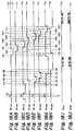
- Fig. 14 which illustrates a second embodiment of the present invention
- every four of the photo/electro conversion portions 1 form one scanning line.
- the vertical shift registers 2 are operated by eight-phase transfer pulse signals ⁇ V1A , ⁇ V2A , ⁇ V3A , ⁇ V4A , ⁇ V1B ⁇ V2B , ⁇ V3B and ⁇ V4B . Therefore, as illustrated in Fig. 15, eight bus lines 10-1, 10-2, 10-3, 10-4, 10-5, 10-6, 10-7 and 10-8 made of aluminum are provided and connected to the transfer electrodes 8 and 9.
- the transfer pulse signals ⁇ V1A , ⁇ V2A , ⁇ V3A , ⁇ V4A , ⁇ V1B , ⁇ V2B , ⁇ V3B and ⁇ V4B are supplied to the bus lines 10-1, 10-2, 10-3, 10-4, 10-5, 10-6, 10-7 and 10-8 respectively.
- the operation of the device of Fig. 14 is interlaced scanning.
- the transfer pulse signals ⁇ V1A , ⁇ V2 , ⁇ V3A , ⁇ V4A , ⁇ V1B , ⁇ V2B , ⁇ V3B , ⁇ V2B , ⁇ V3B and ⁇ V4B are V H , V M , V H , V M , V H , V M , V H and V L , respectively, as shown in Figs. 16A through 16H.
- the signal charges Q A , Q B , Q C , Q D , Q E , Q F , Q G and Q H are read out to the vertical shift register 2.
- the transfer pulse signals ⁇ V1A , ⁇ V2 , ⁇ V3A , ⁇ V4 , ⁇ V1B , ⁇ V2 , ⁇ V3B , ⁇ V2 , ⁇ V3B and ⁇ V4 are V M , V M , V M , V M , V M , V M and V L , respectively, as shown in Figs. 16A through 16H.
- the potential wells are deep as shaded at time t2 in Fig.
- the charges Q A , Q B , Q C and Q D are combined to generate a signal charge Q A + Q B + Q C + Q D in the vertical shift register 2, and the charges Q E , Q F , Q G and Q H are combined to generate a signal charge Q E + Q F + Q G + Q H .
- the transfer pulse signals ⁇ V1A , ⁇ V2A , ⁇ V3A , ⁇ V4A , ⁇ V1B , ⁇ V2B , ⁇ V3B , ⁇ V2B , ⁇ V3B and ⁇ V4B are V M , V M , V M , V M , V M , V L and V L , respectively, as shown in Figs. 16A through 16H.
- the potential wells are deep as shaded at time t3 in Fig. 17.
- the transfer pulse signals ⁇ V1A , ⁇ V2A , ⁇ V3A , ⁇ V4A , ⁇ V1B , ⁇ V2B , ⁇ V3B , ⁇ V2B , ⁇ V3B and ⁇ V4B are V M , V M , V M , V M , V M , V M and V L , respectively, as shown in Figs. 16A through 16H.
- the potential wells are deep as shaded at time t4 in Fig. 17.
- the transfer pulse signals ⁇ V1A , ⁇ V2 , ⁇ V3A , ⁇ V4A , ⁇ V1B , ⁇ V2B , ⁇ V3B , ⁇ V2B , ⁇ V3B and ⁇ V4B are V L , V M , V M , V M , V M , V M and V L , respectively, as shown in Figs. 16A through 16H.
- the potential wells are deep as shaded at time t5 in Fig. 17.
- the vertical shift register 2 performs a one-pixel vertical shift operation upon the signal charge Q A + Q B + Q C + Q D , the signal charge Q E + Q F + Q G + Q H , ⁇ .
- the transfer pulse signals ⁇ V1A , ⁇ V2A , ⁇ V3A , ⁇ V4A , ⁇ V1B , ⁇ V2B , ⁇ V3B and ⁇ V4B are changed to times t6 and t7, time t8 and t9, times t10 and t11, times t12 and t13, times t14 and t15, t16 and t17, and times t18 and t19, in a similar way to times t4 and t5.
- the signal charge Q A + Q B + Q C + Q D is completely transferred to the horizontal output register 3.
- the transfer pulse signals ⁇ V1A , ⁇ V2 , ⁇ V3A , ⁇ V4A , ⁇ V1B , ⁇ V2B , ⁇ V3B , ⁇ V2B , ⁇ V3B and ⁇ V4B are V H , V M , V H , V L , V H , V M , V H and V M , respectively, as shown in Figs. 18A through 18H.
- the signal charges Q A , Q B , Q C , Q D , Q E , Q F , Q G and Q H are read out to the vertical shift register 2.
- the transfer pulse signals ⁇ V1A , ⁇ V2A , ⁇ V3A , ⁇ V4A , ⁇ V1B , ⁇ V2B , ⁇ V3B , ⁇ V2B , ⁇ V3B and ⁇ V4B are V M , V M , V L , V L , V M , V M , V M and V M , respectively, as shown in Figs. 18A through 18H.
- the potential wells are deep as shaded at time t3 in Fig. 19.
- the transfer pulse signals ⁇ V1A , ⁇ V2A , ⁇ V3A , ⁇ V4A , ⁇ V1B , ⁇ V2B , ⁇ V3B , ⁇ V2B , ⁇ V3B and ⁇ V4B are V M , V M , V L , V M , V M , V M , V M and V M , respectively, as shown in Figs. 18A through 18H.
- the potential wells are deep as shaded at time t4 in Fig. 19.
- the transfer pulse signals ⁇ V1A , ⁇ V2 , ⁇ V3A , ⁇ V4A , ⁇ V1B , ⁇ V2B , ⁇ V3B , ⁇ V2B , ⁇ V3B and ⁇ V4B are V M , V M , V M , V L , V L , V M , V M and V M , respectively, as shown in Figs. 18A through 18H.
- the potential wells are deep as shaded at time t5 in Fig. 19.
- the vertical shift register 2 performs a one-pixel vertical shift operation upon the signal charge Q A + Q B , the signal charge Q L + Q D + Q E + Q F , ⁇ .
- the transfer pulse signals ⁇ V1A , ⁇ V2A , ⁇ V3A , ⁇ V4A , ⁇ V1B , ⁇ V2B , ⁇ V3B and ⁇ V4B are changed to times t6 and t7, time t8 and t9, and times t10, in a similar way to times t4 and t5.
- the signal charge Q A + Q B is completely transferred to the horizontal output register 3.
- the transfer pulse signals ⁇ V1A , ⁇ V2A , ⁇ V3A , ⁇ V4A , ⁇ V1B , ⁇ V2B , ⁇ V3B and ⁇ V4B are changed at times t12 and t13, t14 and t15, t16 and t17, t18 and t19, t20 and t21, t22 and t23, t24 and t25, and t26 and t27, in a similar way to times t4 and t5.
- the signal charge Q C + Q D + Q E + Q F is completely transferred to the horizontal output register 3.
- the horizontal output register 3 is designed to process every four rows of the photo/electro conversion portions 1, in other words, the width of the horizontal output register 3 is twice as compared with the prior art.
- the ratio of a width W to a length L of the transfer electrodes 8 and 9 can be twice as compared with the prior art. Therefore, the electric field within the vertical shift registers 2 along the vertical shift direction can be twice as compared with the prior art, and accordingly, the efficiency of charge transfer can be enhanced.
- the signal charge such as Q A + Q B + Q C + Q D is stored in the potential wells beneath four transfer electrodes within the vertical shift register 2 during a vertical shift operation.
- the signal charge such as Q A + Q B + Q C + Q D are stored in the potential wells beneath six or seven transfer electrodes within the vertical shift register 2 during a vertical shift operation. Therefore, the amount of the signal charge in the second embodiment can be about one and half times as large as the amount of the signal charge in the first embodiment as well as in the prior art. Therefore, in the second embodiment, the register blooming can be avoided to broaden the dynamic range.
- the ratio of width to length of the transfer electrodes of the vertical shift registers can be increased, the efficiency of charge transfer can be enhanced.
Landscapes
- Engineering & Computer Science (AREA)
- Multimedia (AREA)
- Signal Processing (AREA)
- Physics & Mathematics (AREA)
- Power Engineering (AREA)
- Electromagnetism (AREA)
- Condensed Matter Physics & Semiconductors (AREA)
- General Physics & Mathematics (AREA)
- Computer Hardware Design (AREA)
- Microelectronics & Electronic Packaging (AREA)
- Transforming Light Signals Into Electric Signals (AREA)
- Solid State Image Pick-Up Elements (AREA)
Abstract
Description
- The present invention relates to a charge coupled device (CCD)type solid state image pickup device.
- Two-dimensional CCD type solid state pickup devices instead of pickup tubes have been used in family video cameras, electronic news gathering (ENG) cameras and the like.
- A prior art CCD type solid state image pickup device includes two-dimensionally arranged photo/electro conversion portions, a plurality of vertical shift registers each connected to one column of the photo/electro conversion portions, and a horizontal output register connected to the vertical shift registers, signal charges of every two of each column of the photo/electro conversion portions are mixed within the vertical shift registers, to creat a mixed signal charge. Then, the mixed signal charge corresponding to two of the photo/electro conversion portions is transferred within the horizontal output register. Thus, one scanning line is formed by every two rows of the photo/electro conversion portions. This will be explained later in detail.
- In the above described prior art CCD type solid state image pickup divice, however, when the density of pixels in the horizontal direction is increased to enhance the resolution, the width of the vertical shift registers is reduced. As a result, the ratio of a width to a length of transfer electrodes of the vertical shift registers is reduced. Therefore, the electric field within the vertical shift registers along the vertical shift direction is reduced, and accordingly, the efficiency of charge transfer is deteriorated.
- It is an object of the present invention to provide a CCD type solid state image pickup device having a high charge transfer efficiency.
- According to the present invention, in a CCD type solid state image pickup device including two-dimensionally arranged photo/electro conversion portions, a plurality of vertical shift registers each connected to one column of the photo/electro conversion portions, and a horizontal output register connected to the vertical shift registers, signal charges of every four of each column of the photo/electro conversion portions are mixed within the vertical shift registers or within the vertical shift registers and the horizontal output register, to create a mixed signal charge. Then, the mixed signal charge corresponding to four of the photo/electro conversion portions is transferred within the horizontal output register. Thus, one scanning line is formed by every four rows of the photo/electro conversion portions. This increases the ratio of a width to a length of transfer electrodes of the vertical shift registers.
- The present invention will be more clearly understood from the description as set forth below, as compared with the prior art, with reference to the accompanying drawings, wherein:
- Fig. 1 is a plan view illustrating a prior art CCD type solid state image pickup device;
- Fig. 2 is a partially enlarged plan view of the device of Fig. 1;
- Figs. 3A, 3B, 3C, 3D, 3E and 3F are timing diagrams for explaining an even field mode operation of the device of Fig. 1;
- Figs. 4A, 4B, 4C and 4D are plan views of the device of Fig. 1 for explaining transfer of signal charge in the even field mode operation;
- Fig. 5 is a diagram for showing transfer of signal charge in the even field mode operation of the device of Fig. 1;
- Figs. 6A, 6B, 6C, 6D, 6E and 6F are timing diagrams for explaining an odd field mode operation of the device of Fig. 1;
- Figs. 7A, 7B, 7C, 7D and 7E are plan views of the device of Fig. 1 for explaining transfer of signal charge in the odd field mode operation;
- Fig. 8A is a diagram for showing transfer of signal charge in the odd field mode operation of the device of Fig. 1;
- Fig. 8B is a plan view illustrating a first embodiment of the CCD type solid state image pickup device according to the present invention;
- Fig. 9 is a partially enlarged plan view of the device of Fig. 8B;
- Figs. 10A through 10J are timing diagrams for explaining an even field mode operation of the device of Fig. 8B;
- Fig. 11 is a diagram for showing transfer of signal charge in the even field mode operation of the device of Fig. 8B;
- Figs. 12A through 12J are timing diagrams for explaining an odd field mode operation of the device of Fig. 8B;
- Fig. 13 is a diagram for showing transfer of signal charge in the odd field mode operation of the device of Fig. 8B;
- Fig. 14 is a plan view illustrating a second embodiment of the CCD type solid state image pickup device according to the present invention;
- Fig. 15 is a partially enlarged plan view of the device of Fig. 14;
- Figs. 16A through 16J are timing diagrams for explaining an even field mode operation of the device of Fig. 14;
- Fig. 17 is a diagram for showing transfer of signal charge in the even field mode operation of the device of Fig. 14;
- Figs. 18A through 18J are timing diagrams for explaining an odd field mode operation of the device of Fig. 14; and
- Fig. 19 is a diagram for showing transfer of signal charge in the odd field mode operation of the device of Fig. 14;
- Before the description of the preferred embodiments, a prior art CCD type solid state image pickup device will be explained with reference to Figs. 1, 2, 3A through 3F, 4A through 4D, 5, 6A through 6F, 7A through 7E, and 8A.
- In Fig. 1, which is a plan view illustrating a prior art CCD type solid state image pickup device, light is incident to two-dimensionally arranged photo/
electro conversion portions 1 formed by photo diodes, and as a result, signal charges obtained by the photo/electro conversion portions 1 are transferred tovertical shift registers 2. The signal charges are further transferred via ahorizontal output register 3 to a signalcharge output register 4 which generates an output voltage Vout. Thevertical shift registers 2 are operated by four-phase transfer pulse signals φ V1, φ V2, φ V3 and φ V4, and thehorizontal output register 3 is operated by two-phase transfer pulse signals φ H1 and φ H2. - In Fig. 1, note that every two rows of the photo/
electro conversion portions 1 form one scanning line. - In Fig. 2, which is a partially enlarged plan view of the device of Fig. 1, each of the photo/
electro conversion portions 1 includes a P+-type impurity diffusion region and an N-type impurity diffusion region formed on a P-type well region of a N-type semiconductor substrate. Thevertical shift registers 2 include N-type buried channels formed on the P-type well region. Provided between the photo/electro conversion portions 1 and thevertical shift registers 2 are readgate regions 5. Every column of the photo/electro portions 1 and thevertical shift registers 2 are isolated from the other columns by a P+-typechannel stopper region 6. - Two
transfer electrodes electro conversion portions 1. In this case, thetransfer electrodes 8 also serve as read gates for the readgate regions 5. Thetransfer electrodes 9 are made of a first polycrystalline silicon layer, and thetransfer electrodes 8 are made of a second polycrystalline silicon layer. - Also, four bus lines 10-1, 10-2, 10-3 and 10-4 made of aluminum are provided and connected to the
transfer electrodes - The operation of the device of Fig. 1 is interlaced scanning.
- An even field mode will now be explained with reference to Figs. 3A through 3F, 4A through 4D, and 5. In this case, assume that signal charges QA, QB, ···, QH are stored in the photo/
electro conversion portions 1 denoted by A, B, ···, H as shown in Fig. 4A. - First, at time tA, the transfer pulse signals φ V1, φ V2, φ V3 and φ V4 are VL, VM, VH and VL, respectively, as shown in Figs. 3A, 3B, 3C and 3D. As a result, the signal charges QA, QC, QE and QG are read out to the
vertical shift register 2 as shown in Fig. 4B. - Next, at time tB, the transfer pulse signals φ V1, φ V2, φ V3 and φ V4 are VH, VL, VL and VM, respectively, as shown in Figs. 3A, 3B, 3C and 3D. As a result, the signal charges QE, QD, QF and QH are read out to the
vertical shift register 2 as shown in Fig. 4C. In this case, the charges QB, QD, QF and QH are added to the charges QA, QC, QE and QG, respectively, to form signal charges QA + QB, QC + QD, QE + QF and QG + QH. - Next, at time t1, the transfer pulse signals φ V1, φ V2, φ V3 and φ V4 are VM, VM, VM and VL, respectively, as shown in Figs. 3A, 3B, 3C and 3D, and as a result, the potential wells are deep as shaded at time t1 in Fig. 5. Subsequently, at time t2, the transfer pulse signals φ V1, φ V2, φ V3 and φ V4 are VL, VM, VM and VL, respectively, as shown in Figs. 3A, 3B, 3C and 3D, and as a result, the potential wells are deep as shaded at time t2 in Fig. 5. Subsequently, at time t3, the transfer pulse signals φ V1, φ V2, φ V3 and φ V4 are VL, VL, VM and VM, respectively, as shown in Figs. 3A, 3B, 3C and 3D, and as a result, the potential wells are deep as shaded at time t3 in Fig. 5. Subsequently, at time t4, the transfer pulse signals φ V1, φ V2, φ V3 and φ V4 are VM, VL, VL and VM, respectively, as shown in Figs. 3A, 3B, 3C and 3D, and as a result, the potential wells are deep as shaded at time t4 in Fig. 5. Subsequently, at time t5, the transfer pulse signals φ V1, φ V2, φ V3 and φ V4 are VM, VM, VL and VL, respectively, as shown in Figs. 3A, 3B, 3C and 3D, and as a result, the potential wells are deep as shaded at time t5 in Fig. 5. Subsequently, at time t6, the transfer pulse signals φ V1, φ V2, φ V3 and φ V4 are VL, VM, VM and VL, respectively, as shown in Figs. 3A, 3B, 3C and 3D, and as a result, the potential wells are deep as shaded at time t6 in Fig. 5. Thus, during a time period from t1 to t6, the
vertical shift register 2 carries out a one-pixel vertical shift operation, so that the signal charge QA + QB is transferred to thehorizontal output register 3 as shown in Fig. 4D. - Then, the transfer pulse signals φ H1 and φ H2 are changed as shown in Figs. 3E and 3F, so that the
horizontal output register 3 performs a one-horizontal line shift operation upon the signal charge QA + QB and the like. - Similarly, the transfer pulse signals φ V1, φ V2, φ V3 and φ V4 are changed at times t7, t8, t9 and t10 in the same way as at times t3, t4, t5 and t6 as shown in Figs. 3A, 3B, 3C and 3D. As a result, the
vertical shift register 2 carries out another one-pixel vertical shift operation, so that the signal charge QC + QD is transferred to thehorizontal output register 3. Then, the transfer pulse signals φ H1 and φ H2 are changed as shown in Figs. 3E and 3F, so that thehorizontal output register 3 performs a one-horizontal line shift operation upon the signal charge QC + QD and the like. - An odd field mode will be explained next with reference to Figs. 6A through 6F, 7A through 7E, and 8. In this case, also assume that signal charges QA, QB, ···, QH are stored in the photo/
electro conversion portions 1 denoted by A, B, ···, H as shown in Fig. 7A. - First, at time tA, the transfer pulse signals φ V1, φ V2, φ V3 and φ V4 are VL, VM, VH and VL, respectively, as shown in Figs. 6A, 6B, 6C and 6D. As a result, the signal charges QA, QC, QE and QG arde read out to the
vertical shift register 2 as shown in Fig. 7B. - Next, at time tB, the transfer pulse signals φ V1, φ V2, φ V3 and φ V4 are VH, VL, VL and VM, respectively, as shown in Figs. 6A, 6B, 6C and 6D. As a result, the signal charges QB, QD, QF and QH arde read out to the
vertical shift register 2 as shown in Fig.4C. In this case, the charges QB, QD and QF are added to the charges QC, QE and QG, respectively, to form signal charges QB + QC, QD + QE and QF + QG. - Next, at time t1, the transfer pulse signals φ V1, φ V2, φ V3 and φ V4 are VM, VM, VM and VL, respectively, as shown in Figs. 6A, 6B, 6C and 6D, and as a result, the potential wells are deep as shaded at time t1 in Fig. 8. Subsequently, at time t2, the transfer pulse signals φ V1, φ V2, φ V3 and φ V4 are VL, VM, VM and VL, respectively, as shown in Figs. 6A, 6B, 6C and 6D, and as a result, the potential wells are deep as shaded at time t2 in Fig. 8. Subsequently, at time t3, the transfer pulse signals φ V1, φ V2, φ V3 and φ V4 are VL, VL, VM and VM, respectively, as shown in Figs. 6A, 6B, 6C and 6D, and as a result, the potential wells are deep as shaded at time t3 in Fig. 8. Subsequently, at time t4, the transfer pulse signals φ V1, φ V2, φ V3 and φ V4 are VM, VL, VL and VM, respectively, as shown in Figs. 6A, 6B, 6C and 6D, and as a result, the potential wells are deep as shaded at time t4 in Fig. 8. Subsequently, at time t5, the transfer-pulse signals φ V1, φ V2, φ V3 and φ V4 are VM, VM, VL and VL, respectively, as shown in Figs. 6A, 6B, 6C and 6D, and as a result, the potential wells are deep as shaded at time t5 in Fig. 8A. Subsequently, at time t6, the transfer pulse signals φ V1, φ V2, φ V3 and φ V4 are VL, VM, VM and VL, respectively, as shown in Figs. 6A, 6B, 6C and 6D, and as a result, the potential wells are deep as shaded at time t6 in Fig. 8A. Thus, during a time period from t1 to t6, the
vertical shift register 2 carries out a one-pixel vertical shift operation, so that the signal charge QA is transferred to thehorizontal output register 3 as shown in Fig. 7D. - Then, the transfer pulse signals φ H1 and φ H2 are changed as shown in Figs. 6E and 6F, so that the
horizontal output register 3 performs a one-horizontal line shift operation upon the signal charge QA and the like. - Similarly, the transfer pulse signals φ V1, φ V2, φ V3 and φ V4 are changed at times t7, t8, t9 and t10 in the same way as at times t3, t4, t5 and t6 as shown in Figs. 6A, 6B, 6C and 6D. As a result, the
vertical shift register 2 carries out another one-pixel vertical shift operation, so that the signal charge QB + QC is transferred to thehorizontal output register 3 as shown in Fig. 7E. Then, the transfer pulse signals φ H1 and φ H2 are changed as shown in Figs. 6E and 6F, so that thehorizontal output register 3 performs a one-horizontal line shift operation upon the signal charge QB + QC and the like. - Then, in the device of Fig. 1, since the resolution in the vertical direction depends upon the number of effective scanning lines in a TV format, signal charges of every two photo/electro conversion portionas (photo diodes) are mixed to generate one horizontal line signal.
- In the device of Fig. 1, however, when the density of pixels in the horizontal direction is increased to enhance the resolution the width of the
vertical shift registers 2 is reduced. As a result, the ratio of a width W to a length L of thetransfer electrodes vertical shift registers 2 along the vertical shift direction is reduced, and accordingly, the efficiency of charge transfer is deteriorated. - In Fig. 8B, which illustrates a first embodiment of the present invention, every four of the photo/
electro conversion portions 1 form one scanning line. In this case, thevertical shift registers 2 may be operated by eight-phase transfer pulse signals; however, thevertical shift registers 2 are operated by six-phase transfer pulse signals φ V1A, φ V2, φ V3A, φ V4, φ V1B and φ V3B. Therefore, as illustrated in Fig. 9, six bus lines 10-1, 10-2, 10-3, 10-4, 10-5 and 10-6 made of aluminum are provided and connected to thetransfer electrodes - The operation of the device of Fig. 8B is interlaced scanning.
- An even field mode will now be explained with reference to Figs. 10A through 10J, and 11. In this case, assume that signal charges QA, QB,···, QH are stored in the photo/
electro conversion portions 1 denoted by A, B, ···, H as shown in Fig. 11A. - First, at time t1, the transfer pulse signals φ V1A, φ V2, φ V3A, φ V4, φ V1B, φ V2, φ V3B, φ V2, φ V3B and φ V4 are VH, VM, VH, VL, VH, VM, VH and VL, respectively, as shown in Figs. 10A through 10H. As a result, the signal charges QA, QB, QC, QD, QE, QF, QG and QH are read out to the
vertical shift register 2. In this case, since the transfer pulse signal φ V4 is VL, the potential wells are deep as shaded at time t1 in Fig. 11, the signal charges QB, QD, and QF never mix with the signal charges QC, QE and QG, respectively. - Next, at time t2, the transfer pulse signals φ V1A, φ V2, φ V3A, φ V4, φ V1B, φ V2, φ V3B, φ V2, φ V3B and φ V4 are VM, VM, VM, VL, VM, VM, VM and VL, respectively, as shown in Figs. 10A through 10H. As a result, the potential wells are deep as shaded at time t2 in Fig. 11, the charges QB, QD, QF and QH are added to the charges QA, QC, QE and QG, respectively, to form signal charges QA + QB, QC + QD, QE + QF and QG + QH.
- Next, at time t3, the transfer pulse signals φ V1A, φ V2, φ V3A, φ V4, φ V1B, φ V2, φ V3B, φ V2, φ V3B and φ V4 are VL, VM, VM, VL, VL, VM, VM and VL, respectively, as shown in Figs. 10A through 10H. As a result, the potential wells are deep as shaded at time t3 in Fig. 11. Subsequently, at time t4, the transfer pulse signals φ V1A, φ V2, φ V3A, φ V4, φ V1B, φ V2, φ V3B, φ V2, φ V3B and φ V4 are VL, VL, VM, VM, VL, VL, VM and VM, respectively, as shown in Figs. 10A through 10H. As a result, the potential wells are deep as shaded at time t4 in Fig. 11. Subsequently, at time t5, the transfer pulse signals φ V1A, φ V2, φ V3A, φ V4, φ V1B, φ V2, φ V3B, φ V2, φ V3B and φ V4 are VM, VL, VL, VM, VM, VL, VL and VM, respectively, as shown in Figs. 10A through 10H. As a result, the potential wells are deep as shaded at time t5 in Fig. 11. Subsequently, at time t6, the transfer pulse signals φ V1A, φ V2, φ V3A, φ V4, φ V1B, φ V2, φ V3B, φ V2, φ V3B and φ V4 are VM, VM, VL, VL, VM, VM, VL and VL, respectively, as shown in Figs. 10A through 10H. As a result, the potential wells are deep as shaded at time t6 in Fig. 11. Subsequently, at time t7, the transfer pulse signals φ V1A, φ V2, φ V3A, φ V4, φ V1B, φ V2 , φ V3B, φ V2, φ V3B and φ V4 are VL, VM, VM, VL, VL, VM, VM and VL, respectively, as shown in Figs. 10A through 10H. As a result, the potential wells are deep as shaded at time t7 in Fig. 11. Subsequently, at time t8, the transfer pulse signals φ V1A, φ V2, φ V3A, φ V4, φ V1B, φ V2, φ V3B, φ V2, φ V3B and φ V4 are VL, VL, VM, VM, VL, VL, VM and VM, respectively, as shown in Figs. 10A through 10H. As a result, the potential wells are deep as shaded at time t8 in Fig. 11. In this state, the signal charge QA + QB is completely transferred to the
horizontal output register 3. - Similarly, the transfer pulse signals φ V1A, φ V2, φ V3A, φ V4, φ V1B, φ V2, φ V3B and φ V4 are changed at times t9, t10, t11 and t12 in the same way as at times t5, t6, t7 and t8 as shown in Figs. 10A through 10H. As a result, the signal charge QC + QD is also completely transferred to the
horizontal output register 3. Therefore, the signal charge QC + QD is added to the signal charge QA + QB in thehorizontal output register 3. - Thus, in the
horizontal output register 3, a signal charge
- Then, the transfer pulse signals φ H1 and φ H2 are changed as shown in Figs. 10I and 10J, so that the
horizontal output register 3 performs a one-horizontal line shift operation upon the signal charge
- An odd field mode will be explained next with reference to Figs. 12A through 12J and 13. In this case, assume that signal charges QA, QB, ···, QH are stored in the photo/
electro conversion portions 1 denoted by A, B, ···, H as shown in Fig. 13. - As shown in Figs. 12A through 12H, from time t1 to time t8, the transfer pulse signals φ V1A, φ V2, φ V3A, φ V4, φ V1B, φ V2, φ V3B, φ V2, φ V3B and φ V4 are changed in the same way as in Figs. 10A through 10H. Therefore, the signal change QA + QB is completely transferred to the
horizontal output register 3 as shown in Fig. 13. - Then, the transfer pulse signals φ H1 and φ H2 are changed as shown in Figs. 12I and 12J, so that the
horizontal output register 3 performs a one-horizontal line shift operation upon the signal charge QA + QB and the like. - Then, at times t9, t10, t11 and t12, the transfer pulse signals φ V1A, φ V2, φ V3A, φ V4, φ V1B, φ V2, φ V3B and φ V4 are changed in the same way as at times t5, t6, t7 and t8 as shown in Figs. 12A through 12H. As a result, the signal charge QC + QD is completely transferred to the
horizontal output register 3 as shown in Fig. 13. - Then, at times t13, t14, t15 and t16, the transfer pulse signals φ V1A, φ V2, φ V3A, φ V4, φ V1B, φ V2, φ V3B and φ V4 are changed in the same way as at times t5, t6, t7 and t8 as shown in Figs. 12A through 12H. As a result, the signal charge QE + QF is also completely transferred to the
horizontal output register 3 as shown in Fig. 13. Therefore, the signal charge QE + QF is added to the signal charge QC + QD in thehorizontal output register 3. - Thus, in the
horizontal output register 3, a signal charge
- Then, the transfer pulse signals φ H1 and φ H2 are changed as shown in Figs. 12I and 12J, so that the
horizontal output register 3 performs a one-horizontal line shift operation upon the signal charge
- In the above-described first embodiment, the
horizontal output register 3 is designed to process every four rows of the photo/electro coversion portions 1, in other words, the width of thehorizontal output register 3 is twice as compared with the prior art. Note that the requirement of size of thehorizontal output register 3 is lenient as compared with the vertical shift registers 2. Thus, in the first embodiment, the ratio of a width W to a length L of the transfer twiceelectrodes vertical shift registers 2 along the vertical shift direction can be twice as compared with the prior art, and accordingly, the efficiency of charge transfer can be enhanced. - In Fig. 14, which illustrates a second embodiment of the present invention, every four of the photo/
electro conversion portions 1 form one scanning line. In this second embodiment, thevertical shift registers 2 are operated by eight-phase transfer pulse signals φ V1A, φ V2A, φ V3A, φ V4A, φ V1B φ V2B, φ V3B and φ V4B. Therefore, as illustrated in Fig. 15, eight bus lines 10-1, 10-2, 10-3, 10-4, 10-5, 10-6, 10-7 and 10-8 made of aluminum are provided and connected to thetransfer electrodes - The operation of the device of Fig. 14 is interlaced scanning.
- An even field mode will now be explained with reference to Figs. 16A through 16J, and 17. In this case, assume that signal charges QA, QB,···, QH are stored in the photo/
electro conversion portions 1 denoted by A, B, ···, H as shown in Fig. 17. - First, at time t1, the transfer pulse signals φ V1A, φ V2, φ V3A, φ V4A, φ V1B, φ V2B, φ V3B, φ V2B, φ V3B and φ V4B are VH, VM, VH, VM, VH, VM, VH and VL, respectively, as shown in Figs. 16A through 16H. As a result, the signal charges QA, QB, QC, QD, QE, QF, QG and QH are read out to the
vertical shift register 2. In this case, since the transfer pulse signal φ V4B is VL, the potential wells are deep as shaded at time t1 in Fig. 17, the signal charges QA, QB, QC and QD never mix with the signal charges QE, QF, QG and QH. - Next, at time t2, the transfer pulse signals φ V1A, φ V2, φ V3A, φ V4, φ V1B, φ V2, φ V3B, φ V2, φ V3B and φ V4 are VM, VM, VM, VM, VM, VM, VM and VL, respectively, as shown in Figs. 16A through 16H. As a result, the potential wells are deep as shaded at time t2 in Fig. 17, the charges QA, QB, QC and QD are combined to generate a signal charge

vertical shift register 2, and the charges QE, QF, QG and QH are combined to generate a signal charge
- Next, at time t3, the transfer pulse signals φ V1A, φ V2A, φ V3A, φ V4A , φ V1B, φ V2B , φ V3B, φ V2B, φ V3B and φ V4B are VM, VM, VM, VM, VM, VM, VL and VL, respectively, as shown in Figs. 16A through 16H. As a result, the potential wells are deep as shaded at time t3 in Fig. 17. Subsequently, at time t4, the transfer pulse signals φ V1A, φ V2A, φ V3A, φ V4A , φ V1B, φ V2B , φ V3B, φ V2B, φ V3B and φ V4B are VM , VM, VM, VM, VM, VM, VM and VL, respectively, as shown in Figs. 16A through 16H. As a result, the potential wells are deep as shaded at time t4 in Fig. 17. Subsequently, at time t5, the transfer pulse signals φ V1A, φ V2, φ V3A, φ V4A, φ V1B, φ V2B, φ V3B, φ V2B, φ V3B and φ V4B are VL, VM, VM, VM , VM, VM, VM and VL, respectively, as shown in Figs. 16A through 16H. As a result, the potential wells are deep as shaded at time t5 in Fig. 17. Thus, at times t3, t4 and t5, the
vertical shift register 2 performs a one-pixel vertical shift operation upon the signal charge

- Similarly, the transfer pulse signals φ V1A, φ V2A, φ V3A, φ V4A, φ V1B, φ V2B , φ V3B and φ V4B are changed to times t6 and t7, time t8 and t9, times t10 and t11, times t12 and t13, times t14 and t15, t16 and t17, and times t18 and t19, in a similar way to times t4 and t5. As a result, the signal charge

horizontal output register 3. - Then, the transfer pulse signals φ H1 and φ H2 are changed as shown in Figs. 16I and 16J, so that the
horizontal output register 3 performs a one-horizontal line shift operation upon the signal charge
- An odd field mode will be explained next with reference to Figs. 18A through 18J, and 19. In this case, assume that signal charges QA, QB,···, QH are stored in the photo/
electro conversion portions 1 denoted by A, B, ···, H as shown in Fig. 19. - First, at time t1, the transfer pulse signals φ V1A, φ V2, φ V3A, φ V4A, φ V1B, φ V2B, φ V3B, φ V2B, φ V3B and φ V4B are VH, VM, VH, VL, VH, VM, VH and VM, respectively, as shown in Figs. 18A through 18H. As a result, the signal charges QA, QB, QC, QD, QE, QF, QG and QH are read out to the
vertical shift register 2. In this case, since the transfer pulse signal φ V4A is VL, the potential wells are deep as shaded at time t1 in Fig. 19, the signal charges QA and QB, QG and QH never mix with the signal charges QC, QD, QE and QF. - Next, at time t3, the transfer pulse signals φ V1A, φ V2A, φ V3A, φ V4A, φ V1B, φ V2B, φ V3B, φ V2B, φ V3B and φ V4B are VM, VM, VL, VL, VM, VM, VM and VM, respectively, as shown in Figs. 18A through 18H. As a result, the potential wells are deep as shaded at time t3 in Fig. 19. Subsequently, at time t4, the transfer pulse signals φ V1A, φ V2A, φ V3A, φ V4A , φ V1B, φ V2B , φ V3B, φ V2B, φ V3B and φ V4B are VM, VM, VL, VM, VM, VM, VM and VM, respectively, as shown in Figs. 18A through 18H. As a result, the potential wells are deep as shaded at time t4 in Fig. 19. Subsequently, at time t5, the transfer pulse signals φ V1A, φ V2, φ V3A, φ V4A, φ V1B, φ V2B, φ V3B, φ V2B, φ V3B and φ V4B are VM, VM, VM, VL, VL, VM, VM and VM, respectively, as shown in Figs. 18A through 18H. As a result, the potential wells are deep as shaded at time t5 in Fig. 19. Thus, at times t3, t4 and t5, the
vertical shift register 2 performs a one-pixel vertical shift operation upon the signal charge QA + QB, the signal charge
- Similarly, the transfer pulse signals φ V1A, φ V2A, φ V3A, φ V4A, φ V1B, φ V2B , φ V3B and φ V4B are changed to times t6 and t7, time t8 and t9, and times t10, in a similar way to times t4 and t5. As a result, the signal charge QA + QB is completely transferred to the
horizontal output register 3. - Then, the transfer pulse signals φ H1 and φ H2 are changed as shown in Figs. 18I and 18J, so that the
horizontal output register 3 performs a one-horizontal line shift operation upon the signal charge QA + QB and the like. - Next, the transfer pulse signals φ V1A, φ V2A, φ V3A, φ V4A, φ V1B, φ V2B, φ V3B and φ V4B are changed at times t12 and t13, t14 and t15, t16 and t17, t18 and t19, t20 and t21, t22 and t23, t24 and t25, and t26 and t27, in a similar way to times t4 and t5. As a result, the signal charge

horizontal output register 3. Then, the transfer pulse signals φ H1 and φ H2 are changed as shown in Figs. 18I and 18J, so that thehorizontal output register 3 performs a one-horizontal line shift operation upon the signal charge
- Also, the above-described second embodiment, the
horizontal output register 3 is designed to process every four rows of the photo/electro conversion portions 1, in other words, the width of thehorizontal output register 3 is twice as compared with the prior art. - Thus, in the second embodiment, the ratio of a width W to a length L of the
transfer electrodes vertical shift registers 2 along the vertical shift direction can be twice as compared with the prior art, and accordingly, the efficiency of charge transfer can be enhanced. - Further, in the first embodiment, the signal charge such as

vertical shift register 2 during a vertical shift operation. On the other hand, in the second embodiment, the signal charge such as
vertical shift register 2 during a vertical shift operation. Therefore, the amount of the signal charge in the second embodiment can be about one and half times as large as the amount of the signal charge in the first embodiment as well as in the prior art. Therefore, in the second embodiment, the register blooming can be avoided to broaden the dynamic range. - As explained hereinabove, according to the present invention, since the ratio of width to length of the transfer electrodes of the vertical shift registers can be increased, the efficiency of charge transfer can be enhanced.
Claims (6)
- A CCD type solid state image pickup device comprising:two-dimensionally arranged photo/electro conversion portions (1) in rows, columns;a plurality of vertical shift registers (2) each connected to one column of said photo/electro conversion portions;a horizontal output register (3) connected to said vertial transfer portions;means for transferring first signal charges (QA, QB, QC, QD ···) of each column of said photo/electro conversion portions to one of said vertical shift registers, so that every two of said first signal charges are combined into one of second signal charges (
 means for transferring said second signal charge from said vertical shift registers to said horizontal output register, so that every two of said second signal charges are combined into one of third signal charges (
 means for transferring said third signal charges within said horizontal output register.
 - The device as set forth in claim 1, wherein each of said vertical shift registers comprises:a plurality of first transfer electrodes (8) each corresponding to one of said photo/electro conversion portions; anda plurality of second transfer electrodes (9) each adjacent to one of said first transfer electrodes,said first transfer electrodes being four-phase operated,
said second transfer electrodes being two-phase operated. - The device as set forth in claim 1, further comprising an interlacing means for changing a combination of said second signal charges in said third signal charges to generate an even field image and an odd field image from said horizontal output register.
- A CCD type solid state image pickup device comprising:two-dimensionally arranged photo/electro conversion portions (1) in rows, columns;a plurality of vertical shift registers (2) each connected to one column of said photo/electro conversion portions;a horizontal output register (3) connected to said vertial transfer portions;means for transferring said second signal charges from said vertical shift registers to said horizontal output register, so that every two of said second signal charges are combined into one of third signal charges (
 means for transferring said second signal charge from said vertical shift registers to said horizontal output register; andmeans for transferring said second signal charges within said horizontal output register.
 - The device as set forth in claim 4, wherein eachof said vertical shift registers comprises: a plurality of first transfer electrodes (8) each corresponding to one of said photo/electro conversion portions; anda plurality of second transfer electrodes (9) each adjacent to one of said first transfer electrodes,said first transfer electrodes being four-phase operated,
said second transfer electrodes being four-phase operated. - The device as set forth in claim 4, further comprising an interlacing means for changing a combination of said first signal charges in said second signal charges to generate an even field image and an odd field image from said horizontal output register.
Applications Claiming Priority (2)
| Application Number | Priority Date | Filing Date | Title |
|---|---|---|---|
| JP7133697A JP2865019B2 (en) | 1995-05-31 | 1995-05-31 | Driving method of charge transfer solid-state imaging device |
| JP133697/95 | 1995-05-31 |
Publications (2)
| Publication Number | Publication Date |
|---|---|
| EP0746144A2 true EP0746144A2 (en) | 1996-12-04 |
| EP0746144A3 EP0746144A3 (en) | 1998-12-23 |
Family
ID=15110775
Family Applications (1)
| Application Number | Title | Priority Date | Filing Date |
|---|---|---|---|
| EP96108795A Withdrawn EP0746144A3 (en) | 1995-05-31 | 1996-05-31 | CCD type solid state image pickup device |
Country Status (5)
| Country | Link |
|---|---|
| US (1) | US5686742A (en) |
| EP (1) | EP0746144A3 (en) |
| JP (1) | JP2865019B2 (en) |
| KR (1) | KR100206692B1 (en) |
| TW (1) | TW305094B (en) |
Cited By (3)
| Publication number | Priority date | Publication date | Assignee | Title |
|---|---|---|---|---|
| EP0896468A2 (en) * | 1997-08-07 | 1999-02-10 | Nec Corporation | Solid state imaging device and method for driving the same |
| EP1063844A1 (en) * | 1998-02-10 | 2000-12-27 | Nikon Corporation | Method of driving solid-state imaging device, imaging device, alignment device, and aligning method |
| GB2370712A (en) * | 2000-10-31 | 2002-07-03 | Hewlett Packard Co | Photosensor array with decreased scan time for decreased resolution |
Families Citing this family (11)
| Publication number | Priority date | Publication date | Assignee | Title |
|---|---|---|---|---|
| JP3887878B2 (en) * | 1997-06-03 | 2007-02-28 | ソニー株式会社 | Method and apparatus for measuring dark signal level of solid-state imaging device |
| JPH11164205A (en) * | 1997-11-28 | 1999-06-18 | Sony Corp | Solid-state image pickup device and its drive method |
| JP3302927B2 (en) * | 1998-07-03 | 2002-07-15 | 日本電気株式会社 | Solid-state imaging device and driving method thereof |
| KR100606408B1 (en) * | 1998-12-12 | 2006-11-30 | 엘지.필립스 엘시디 주식회사 | Apparatus for Taking Image |
| KR100570961B1 (en) * | 1998-12-12 | 2006-08-30 | 엘지.필립스 엘시디 주식회사 | Apparatus for Taking Image |
| JP3967500B2 (en) * | 1999-09-08 | 2007-08-29 | 富士フイルム株式会社 | Solid-state imaging device and signal readout method |
| JP4294810B2 (en) * | 1999-09-10 | 2009-07-15 | 富士フイルム株式会社 | Solid-state imaging device and signal readout method |
| JP2001111026A (en) * | 1999-10-07 | 2001-04-20 | Fuji Film Microdevices Co Ltd | Solid state image sensor |
| JP5133292B2 (en) * | 2009-04-13 | 2013-01-30 | ソニー株式会社 | Solid-state imaging device, driving method thereof, and camera system |
| JP5133293B2 (en) * | 2009-04-13 | 2013-01-30 | ソニー株式会社 | Solid-state imaging device, driving method thereof, and camera system |
| JP5126385B2 (en) * | 2011-05-02 | 2013-01-23 | ソニー株式会社 | Solid-state imaging device, driving method thereof, and camera system |
Citations (1)
| Publication number | Priority date | Publication date | Assignee | Title |
|---|---|---|---|---|
| EP0594411A2 (en) * | 1992-10-21 | 1994-04-27 | Sharp Kabushiki Kaisha | A solid-stade imaging device and a method for driving the same |
Family Cites Families (4)
| Publication number | Priority date | Publication date | Assignee | Title |
|---|---|---|---|---|
| US4803710A (en) * | 1986-01-09 | 1989-02-07 | General Electric Company | Storage registers with charge packet accumulation capability, as for solid-state imagers |
| JP2853216B2 (en) * | 1989-11-09 | 1999-02-03 | 日本電気株式会社 | Solid-state imaging device |
| JP2614129B2 (en) * | 1990-02-16 | 1997-05-28 | 富士写真フイルム株式会社 | Electronic still camera |
| DE69332769T2 (en) * | 1992-11-20 | 2003-08-14 | Matsushita Electric Ind Co Ltd | Method for controlling a solid-state image sensor |
-
1995
- 1995-05-31 JP JP7133697A patent/JP2865019B2/en not_active Expired - Fee Related
-
1996
- 1996-05-31 US US08/656,470 patent/US5686742A/en not_active Expired - Fee Related
- 1996-05-31 KR KR1019960019042A patent/KR100206692B1/en not_active IP Right Cessation
- 1996-05-31 EP EP96108795A patent/EP0746144A3/en not_active Withdrawn
- 1996-06-05 TW TW085106818A patent/TW305094B/zh active
Patent Citations (1)
| Publication number | Priority date | Publication date | Assignee | Title |
|---|---|---|---|---|
| EP0594411A2 (en) * | 1992-10-21 | 1994-04-27 | Sharp Kabushiki Kaisha | A solid-stade imaging device and a method for driving the same |
Cited By (10)
| Publication number | Priority date | Publication date | Assignee | Title |
|---|---|---|---|---|
| EP0896468A2 (en) * | 1997-08-07 | 1999-02-10 | Nec Corporation | Solid state imaging device and method for driving the same |
| EP0896468A3 (en) * | 1997-08-07 | 2000-05-17 | Nec Corporation | Solid state imaging device and method for driving the same |
| US6185270B1 (en) | 1997-08-07 | 2001-02-06 | Nec Corporation | Solid state imaging device and method for driving the same |
| CN1133317C (en) * | 1997-08-07 | 2003-12-31 | 恩益禧电子股份有限公司 | Solid state imaging device and method for driving the same |
| EP1063844A1 (en) * | 1998-02-10 | 2000-12-27 | Nikon Corporation | Method of driving solid-state imaging device, imaging device, alignment device, and aligning method |
| EP1063844A4 (en) * | 1998-02-10 | 2007-07-11 | Nikon Corp | Method of driving solid-state imaging device, imaging device, alignment device, and aligning method |
| GB2370712A (en) * | 2000-10-31 | 2002-07-03 | Hewlett Packard Co | Photosensor array with decreased scan time for decreased resolution |
| US6765699B1 (en) | 2000-10-31 | 2004-07-20 | Hewlett-Packard Development Company, L.P. | Photosensor array with decreased scan time for decreased optical sampling rates |
| GB2370712B (en) * | 2000-10-31 | 2004-08-25 | Hewlett Packard Co | Photosensor array with decreased scan time for decreased optical sampling rates |
| US6791726B2 (en) | 2000-10-31 | 2004-09-14 | Hewlett-Packard Development Company, L.P. | Photosensor array with decreased scan time for decreased optical sampling rates |
Also Published As
| Publication number | Publication date |
|---|---|
| KR100206692B1 (en) | 1999-07-01 |
| KR960043789A (en) | 1996-12-23 |
| US5686742A (en) | 1997-11-11 |
| JP2865019B2 (en) | 1999-03-08 |
| JPH08330563A (en) | 1996-12-13 |
| EP0746144A3 (en) | 1998-12-23 |
| TW305094B (en) | 1997-05-11 |
Similar Documents
| Publication | Publication Date | Title |
|---|---|---|
| US5686742A (en) | CCD type solid state image pickup device having high charge transfer efficiency | |
| US6075565A (en) | Solid-state image sensing apparatus and its driving method | |
| US4598321A (en) | CCD imagers with registers partitioned for simultaneous charge transfers in opposing directions | |
| EP0313322B1 (en) | Solid-state image sensor having a plurality of horizontal transfer portions | |
| JPS5984575A (en) | Solid-state image-pickup element | |
| KR890005237B1 (en) | Solide - state imaging device / jp | |
| GB2128052A (en) | Flicker reduction in field-interlaced three-phase clocked ccd imagers | |
| JP2983401B2 (en) | Charge transfer method, charge transfer device, and solid-state imaging device using the same | |
| US4675887A (en) | Solid state imaging device and method with row-by-row charge transfer | |
| JPH05199465A (en) | Charge-coupled image sensing device and camera having such image sensing device | |
| EP0869665B1 (en) | Solid state image sensor | |
| JPS62208668A (en) | Charge transfer type solid-state image sensing element | |
| EP0520605B1 (en) | A solid-state imaging device and a method for driving same | |
| US6355949B1 (en) | Solid state imaging apparatus with horizontal charge transfer register which can transfer signal charge faster | |
| JPH07322143A (en) | Method for driving solid-state image pickup device | |
| JPS60217761A (en) | High-resolution solid-state image pickup device | |
| JP3036250B2 (en) | CCD element | |
| JP2623150B2 (en) | Solid-state imaging device | |
| JP4419275B2 (en) | Solid-state imaging device, driving method thereof, and image input device | |
| JP2001060681A (en) | Solid-state image pickup device and method for driving the same | |
| JPS6046594B2 (en) | How to drive a charge transfer image sensor | |
| JP2001094740A (en) | Solid-state image pickup device, its drive method and image input device | |
| JP3008629B2 (en) | Solid-state imaging device | |
| JP3158324B2 (en) | Driving method of solid-state imaging device | |
| JPH09129861A (en) | Solid state image sensing element |
Legal Events
| Date | Code | Title | Description |
|---|---|---|---|
| PUAI | Public reference made under article 153(3) epc to a published international application that has entered the european phase |
Free format text: ORIGINAL CODE: 0009012 |
|
| AK | Designated contracting states |
Kind code of ref document: A2 Designated state(s): DE FR GB |
|
| PUAL | Search report despatched |
Free format text: ORIGINAL CODE: 0009013 |
|
| AK | Designated contracting states |
Kind code of ref document: A3 Designated state(s): DE FR GB |
|
| 17P | Request for examination filed |
Effective date: 19990301 |
|
| 17Q | First examination report despatched |
Effective date: 20021021 |
|
| RAP1 | Party data changed (applicant data changed or rights of an application transferred) |
Owner name: NEC ELECTRONICS CORPORATION |
|
| GRAP | Despatch of communication of intention to grant a patent |
Free format text: ORIGINAL CODE: EPIDOSNIGR1 |
|
| STAA | Information on the status of an ep patent application or granted ep patent |
Free format text: STATUS: THE APPLICATION HAS BEEN WITHDRAWN |
|
| 18W | Application withdrawn |
Effective date: 20031204 |