EP0745997A2 - Dispositif à charge couplée à haut rendement de transfert de charge - Google Patents
Dispositif à charge couplée à haut rendement de transfert de charge Download PDFInfo
- Publication number
- EP0745997A2 EP0745997A2 EP96108667A EP96108667A EP0745997A2 EP 0745997 A2 EP0745997 A2 EP 0745997A2 EP 96108667 A EP96108667 A EP 96108667A EP 96108667 A EP96108667 A EP 96108667A EP 0745997 A2 EP0745997 A2 EP 0745997A2
- Authority
- EP
- European Patent Office
- Prior art keywords
- electrodes
- semiconductor region
- semiconductor
- nonactive
- type semiconductor
- Prior art date
- Legal status (The legal status is an assumption and is not a legal conclusion. Google has not performed a legal analysis and makes no representation as to the accuracy of the status listed.)
- Granted
Links
Images


Classifications
-
- G—PHYSICS
- G11—INFORMATION STORAGE
- G11C—STATIC STORES
- G11C19/00—Digital stores in which the information is moved stepwise, e.g. shift registers
- G11C19/28—Digital stores in which the information is moved stepwise, e.g. shift registers using semiconductor elements
- G11C19/282—Digital stores in which the information is moved stepwise, e.g. shift registers using semiconductor elements with charge storage in a depletion layer, i.e. charge coupled devices [CCD]
- G11C19/285—Peripheral circuits, e.g. for writing into the first stage; for reading-out of the last stage
Definitions
- the present invention relates to a charge coupled device.
- a prior art charge coupled device includes a semiconductor substrate having a semiconductor region, a plurality of nonactive barrier electrodes, a plurality of first electrodes and a plurality of second electrodes arranged between the nonactive barrier electrodes. Also, a floating diffusion region is provided as an output portion (see: JP-A-6-314706). This will be explained later in detail.
- the width of the floating diffusion region is smaller than the width of the semiconductor region, to enhance the sensibility of detection of signal charge. Further, in order to obtain a full amount of signal charge in the direction of the signal flow, the outermost one of the first electrodes is made long. As a result, the efficiency of transfer of charge in the direction of the signal flow is reduced.
- a charge coupled device including a semiconductor substrate having a semiconductor region, a plurality of nonactive barrier electrodes, a plurality of first electrodes and a plurality of second electrodes arranged between the nonactive barrier electrodes, an outermost one of the nonactive barrier electrodes is electrically isolated from the others of the nonactive barrier electrodes.
- a first voltage is applied to the outermost nonactive barrier electrode and a second voltage different from the first voltage is applied to the other nonactive barrier electrode, the direction of transfer of signal charge is clearly determined.
- Fig. 1A is a cross-sectional view illustrating a prior art buried channel charge coupled device
- Fig. 1B is a plan view of Fig. 1A.
- Fig. 1A is a cross-sectional view taken along the line A-A of Fig. 1B (see: JP-A-6-314706).
- reference numeral 1 designates a P-type semiconductor substrate on which N-type semiconductor regions 2-1, 2-2, ⁇ , and N - -type semiconductor regions 3-1, 3-2, ⁇ therebetween are formed. Also, an N + -type semiconductor region 4 is formed as a floating diffusion region on the semiconductor substrate 1 adjacent to the outermost N-type semiconductor region 2-1. Further, an N-type semiconductor region 5, an N + -type semiconductor region 6 for receiving a reference voltage V R , and a grounded P + -type semiconductor region 7 serving as an isolation region are formed on the semiconductor substrate 1. Note that the floating diffusion region 4 is connected to a source follower 8 which generates an output voltage V out .
- electrodes E0 for receiving a constant voltage V M are formed via an insulating layer (not shown) on the half of each of the N-type semiconductor regions 2-1, 2-2, ⁇ .
- electrodes E1 for receiving a pulse voltage ⁇ 1 are formed via an insulating layer (not shown) on the half of each of the N-type semiconductor regions 2-1, 2-3, ⁇ and on the N - -type semiconductor regions 3-1, 3-3, ⁇ .
- Further electrodes E2 for receiving a pulse voltage ⁇ 2 are formed via an insulating layer (not shown) on the half of each of the N-type semiconductor regions 2-2, 2-4, ⁇ and on the N - -type semiconductor regions 3-2, 3-4, ⁇ .
- an electrode E3 for receiving a reset voltage ⁇ R is formed via an insulating layer (not shown) on the N-type semiconductor region 4.
- Figs. 1A and 1B The operation of the buried channel charge coupled device of Figs. 1A and 1B is explained with reference to Figs. 2A and 2B and Figs. 3A, 3B and 3C.
- the pulse voltages ⁇ 1 and ⁇ 2 are changed as shown in Fig. 2A to carry out a two-phase operation.
- V H is a high level of the pulse voltages ⁇ 1 and ⁇ 2
- V L is a low level of the pulse voltages ⁇ 1 and ⁇ 2 .
- the voltage V M applied to the electrodes E0 is between V H and V L , and the electrodes E0 serve as nonactive barrier electrodes.
- the reset voltage ⁇ R applied to the electrode E3 is changed as shown in Fig. 2B. That is, the potential at the N + -type semiconductor region 4 is the same as that at the N + -type semiconductor region 6 at every one two-phase operation.
- the potential within the device is shown in Fig. 3A. That is, the potential wells within the regions 3-2, 2-2, 3-1 and 2-1 induced by the pulse voltages ⁇ 1 and ⁇ 2 are deeper in the direction of the signal flow. As a result, signal charge Q 1 is stored in the potential well of the N-type semiconductor region 2-1. Similarly, signal charge Q 2 is stored in the potential well of the N-type semiconductor region 2-3.
- the control enters a state II where the pulse voltages ⁇ 1 and ⁇ 2 are V L and V H , respectivly, the potential within the device is shown in Fig. 3B, That is, the potential wells within the regions 3-1, 2-1 and 4 are deeper in the direction of the signal flow.
- the signal charge Q 1 is transferred from the potential well of the N-type semiconductor region 2-1 to the potential well of the N-type semiconductor region 4.
- the signal charge Q 2 is transferred from the potential well of the N-type semiconductor region 2-3 to the potential well of the N-type semiconductor region 2-2
- signal charge Q 3 is transferred from the potential well of the N-type semiconductor region 2-5 (not shown) to the potential well of the N-type semiconductor region 2-4.
- control enters a state III where the reset voltage ⁇ R is made high, the potential at the N + -type semiconductor region 4 is again the same as that at the N + -type semiconductor region 6 to prepare the detection of the next signal charge as shown in Fig. 3C.
- a width W' of the N + -type semiconductor region (floating diffusion region) 4 is smaller than a width W of the semiconductor regions 3-1, 2-2, 3-2, 2-3, 3-3, ⁇ , to enhance the sensibility of detection of signal charge.
- the maximum storage amount of charge by the shaded well S1 of the N-type semiconductor region 2-1 should be equalized with that by the shaded well S2 of the N-type semiconductor region 2-2, that is, the area of the shaded well S1 should be the same as that of the shaded well S2.
- the length L10 of the shaded well S1 is longer than the length L20 of the shaded well S2, and accordingly, the length L1 of the outermost electrode Ei is longer than the length L2 of the outermost electrode E2. That is, L1 > L2 This reduced the efficiency of transfer of charge in the direction of the signal flow.
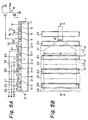
- Fig. 5A is a cross-sectional view illustrating an embodiment of the charge coupled device according to the present invention
- Fig. 5B is a plan view of Fig. 5B.
- Fig. 5A is a cross-sectional view taken along the line A-A of Fig. 5B.
- E0' the outermost electrode of the electrodes E0 of Figs. 1A and 1B denoted by E0' is electrically isolated from the other electrodes E0, and a voltage V M ', which is different from the voltage V M , is applied to the electrode E0'.
- the outermost electrode E1 of Figs. 1A and 1B is replaced by an electrode E1' whose length L1' is smaller than the length L1 of the electrode E1.
- the length L1' of the electrode E1 is L1' ⁇ L2
- the electrode E0' also serves as a nonactive barrier electrode.
- the voltage V M ' applied to the electrode E0' is higher than the voltage V M applied to the electrodes E0, so that the potential well within the region 2'-1 beneath the electrode E0' is deeper the potential well within the regions 2-2, 2-3, ⁇ beneath the electrodes E0.
- the transfer operation of the device of Figs. 5A and 5B is carried out by changing the pulse voltages ⁇ 1 and ⁇ 2 and the reset voltage ⁇ R as shown in Figs. 6A and 6B.
- the potential within the device is shown in Fig. 7A. That is, the potential wells within the regions 3-2, 2-2, 3-1 and 2'-1 induced by the pulse voltages ⁇ 1 and ⁇ 2 are deeper in the direction of the signal flow. As a result, signal charge Q 1 is stored in the potential well of the N-type semiconductor region 2-1. Similarly, signal charge Q 2 is stored in the potential well of the N-type semiconductor region 2-3.
- the control enters a state II where the pulse voltages ⁇ 1 and ⁇ 2 are V L and V H , respectively, the potential within the device is shown in Fig. 7B, That is, the potential wells within the regions 3-1, 2'-1 and 4 are deeper in the direction of the signal flow.
- the signal charge Q 1 is transferred from the potential well of the N-type semiconductor region 2-1 to the potential well of the N-type semiconductor region 4.
- the length L1' of the electrode E1' can be reduced, the efficiency of transfer of charge can be enhanced. This will be explained later in detail.
- the signal charge Q 2 is transferred from the potential well of the N-type semiconductor region 2-3 to the potential well of the N-type semiconductor region 2-2, and signal charge Q 3 is transferred from the potential well of the N-type semiconductor region 2-5 (not shown) to the potential well of the N-type semiconductor region 2-4.
- an impedance transformation is performed upon the signal charge Q 1 at the N + -type semiconductor region (floating diffusion region) 4 by the source follower 8, to generate the output voltage V out .
- control enters a state III where the reset voltage ⁇ R is made high, the potential at the N + -type semiconductor region 4 is again the same as that at the N + -type semiconductor region 6 to prepare the detection of the next signal charge as shown in Fig. 7C.
- Fig. 8A when the amount of signal charge A is small, the small length L10' of the potential well the N-type semiconductor region 2'-1 beneath the electrode E1' enhances the efficiency of transfer of charge in the direction of the signal flow.
- Fig. 8B when excess signal charge C in addition to large signal charge B is stored in the potential wells beneath the electrode E1 (L1'), region 2'-1, all of the signal charge C may be transferred to the direction of the signal flow, since the potential well beneath the electrode E0' is deeper than the potential well beneath the electrode E0. This contributes to the enhancement of the efficiency of transfer of charge in the direction of the signal flow.
- the regions 2'-1, 2-2, 2-3, 2-4, ⁇ are denoted by N
- the regions 3-1, 3-2, 3-3, ⁇ are denoted by N - .
- the regions 2'-1, 2-2, 2-3, 2-4, ⁇ are denoted by N +
- the regions 3-1, 3-2, 3-3, ⁇ can be denoted by N. That is, if the concentration of N-type impurity of the regions 2'-2, 2-2, 2-3, 2-4, ⁇ larger than that of N-type impurity of the regions 3-1, 3-2, 3-3, 3-4, ⁇ , the direction of the signal flow can be determined.
- the present invention can be applied to a surface channel charge coupled device as illustrated in Fig. 9.
- the regions 2'-1, 2-2, 2-3, 2-4, ⁇ , and 3-1, 3-2, 3-3, 3-4, ⁇ are of a P-type.
- the concentration of P-type impurity of the regions 2'-2, 2-2, 2-3, 2-4, ⁇ smaller than that of P-type impurity of the regions 3-1, 3-2, 3-3, 3-4, ⁇ , the direction of the signal flow can be determined.
- the present invention can be applied to a P-channel type buried channel charge coupled device as illustrated in Fig. 10, where the polarity of conductivity is reversed, so that holes are transferred.
- Fig. 10 the pulse voltages ⁇ 1 and ⁇ 2 and the reset voltage ⁇ R are changed as shown in Figs. 11A and 11B.
- the efficiency of transfer of charge can be enhanced.
Landscapes
- Solid State Image Pick-Up Elements (AREA)
- Transforming Light Signals Into Electric Signals (AREA)
Applications Claiming Priority (3)
| Application Number | Priority Date | Filing Date | Title |
|---|---|---|---|
| JP7133151A JP2768311B2 (ja) | 1995-05-31 | 1995-05-31 | 電荷転送装置 |
| JP13315195 | 1995-05-31 | ||
| JP133151/95 | 1995-05-31 |
Publications (3)
| Publication Number | Publication Date |
|---|---|
| EP0745997A2 true EP0745997A2 (fr) | 1996-12-04 |
| EP0745997A3 EP0745997A3 (fr) | 1999-01-07 |
| EP0745997B1 EP0745997B1 (fr) | 2002-08-14 |
Family
ID=15097908
Family Applications (1)
| Application Number | Title | Priority Date | Filing Date |
|---|---|---|---|
| EP96108667A Expired - Lifetime EP0745997B1 (fr) | 1995-05-31 | 1996-05-30 | Dispositif à charge couplée à haut rendement de transfert de charge |
Country Status (6)
| Country | Link |
|---|---|
| US (1) | US5796801A (fr) |
| EP (1) | EP0745997B1 (fr) |
| JP (1) | JP2768311B2 (fr) |
| KR (1) | KR100249412B1 (fr) |
| DE (1) | DE69622929D1 (fr) |
| TW (1) | TW297953B (fr) |
Families Citing this family (5)
| Publication number | Priority date | Publication date | Assignee | Title |
|---|---|---|---|---|
| JP2768312B2 (ja) * | 1995-06-02 | 1998-06-25 | 日本電気株式会社 | 電荷転送装置、その駆動方法及び製造方法 |
| US5929471A (en) * | 1997-05-30 | 1999-07-27 | Dalsa, Inc. | Structure and method for CCD sensor stage selection |
| US6586784B1 (en) * | 2002-10-02 | 2003-07-01 | Eastman Kodak Company | Accumulation mode clocking of a charge-coupled device |
| US7952633B2 (en) * | 2004-11-18 | 2011-05-31 | Kla-Tencor Technologies Corporation | Apparatus for continuous clocking of TDI sensors |
| US7880782B2 (en) * | 2008-05-30 | 2011-02-01 | Eastman Kodak Company | Image sensor clocking method |
Citations (1)
| Publication number | Priority date | Publication date | Assignee | Title |
|---|---|---|---|---|
| US5521405A (en) * | 1993-04-30 | 1996-05-28 | Nec Corporation | Charge transfer device with two-phase two-layered electrode structure and method for fabricating the same |
Family Cites Families (8)
| Publication number | Priority date | Publication date | Assignee | Title |
|---|---|---|---|---|
| US4178519A (en) * | 1978-08-16 | 1979-12-11 | General Electric Company | Input circuit for charge transfer apparatus |
| US4896340A (en) * | 1985-11-01 | 1990-01-23 | Hughes Aircraft Company | Partial direct injection for signal processing system |
| JPS63122271A (ja) * | 1986-11-12 | 1988-05-26 | Hitachi Ltd | 電荷転送素子 |
| US5065203A (en) * | 1988-07-07 | 1991-11-12 | Tektronix, Inc. | Trench structured charge-coupled device |
| JPH0728031B2 (ja) * | 1989-02-11 | 1995-03-29 | 日本電気株式会社 | 電荷転送装置 |
| JP3070146B2 (ja) * | 1991-06-19 | 2000-07-24 | ソニー株式会社 | 固体撮像装置 |
| JPH05211180A (ja) * | 1991-09-26 | 1993-08-20 | Toshiba Corp | 電荷転送装置 |
| KR950002084A (ko) * | 1993-06-22 | 1995-01-04 | 오가 노리오 | 전하전송장치 |
-
1995
- 1995-05-31 JP JP7133151A patent/JP2768311B2/ja not_active Expired - Lifetime
-
1996
- 1996-05-30 DE DE69622929T patent/DE69622929D1/de not_active Expired - Lifetime
- 1996-05-30 EP EP96108667A patent/EP0745997B1/fr not_active Expired - Lifetime
- 1996-05-31 US US08/655,910 patent/US5796801A/en not_active Expired - Fee Related
- 1996-05-31 KR KR1019960018972A patent/KR100249412B1/ko not_active IP Right Cessation
- 1996-06-03 TW TW085106612A patent/TW297953B/zh active
Patent Citations (1)
| Publication number | Priority date | Publication date | Assignee | Title |
|---|---|---|---|---|
| US5521405A (en) * | 1993-04-30 | 1996-05-28 | Nec Corporation | Charge transfer device with two-phase two-layered electrode structure and method for fabricating the same |
Also Published As
| Publication number | Publication date |
|---|---|
| TW297953B (fr) | 1997-02-11 |
| US5796801A (en) | 1998-08-18 |
| JPH08330573A (ja) | 1996-12-13 |
| JP2768311B2 (ja) | 1998-06-25 |
| DE69622929D1 (de) | 2002-09-19 |
| KR100249412B1 (ko) | 2000-03-15 |
| EP0745997B1 (fr) | 2002-08-14 |
| EP0745997A3 (fr) | 1999-01-07 |
Similar Documents
| Publication | Publication Date | Title |
|---|---|---|
| EP0495523A1 (fr) | Capteur d'image à CCD linéaire | |
| US4060738A (en) | Charge coupled device random access memory | |
| JPH084136B2 (ja) | 電荷転送装置 | |
| US3996600A (en) | Charge coupled optical scanner with blooming control | |
| EP0191587B1 (fr) | Dispositifs à transfert de charges | |
| US4727560A (en) | Charge-coupled device with reduced signal distortion | |
| EP0745997A2 (fr) | Dispositif à charge couplée à haut rendement de transfert de charge | |
| US5892251A (en) | Apparatus for transferring electric charges | |
| US4814844A (en) | Split two-phase CCD clocking gate apparatus | |
| US4356502A (en) | Protection circuit for a semiconductor device | |
| EP0161023B1 (fr) | Dispositif semi-conducteur à couplage de charges avec commande dynamique | |
| US4649407A (en) | Charge coupled device for transferring electric charge | |
| US4691218A (en) | Charge transfer device | |
| US5502318A (en) | Bipolar gate charge coupled device with clocked virtual phase | |
| US4374334A (en) | Signal comparator apparatus | |
| US4272693A (en) | Analysis circuit for a charge coupled device | |
| US4223329A (en) | Bipolar dual-channel charge-coupled device | |
| US5172399A (en) | Semiconductor charge transfer device including charge quantity detection | |
| JP3060649B2 (ja) | 半導体装置及びその駆動方法 | |
| US5204989A (en) | Charge sensing device | |
| US6191440B1 (en) | Charge transfer device with improved charge detection sensitivity | |
| US4058716A (en) | Surface charge signal processing apparatus | |
| US4726049A (en) | Charge-coupled device input with complementary signal-dependent charge packets | |
| EP0073019A2 (fr) | Dispositif à mémoire et son procédé de fabrication | |
| JP2723054B2 (ja) | 電荷転送素子 |
Legal Events
| Date | Code | Title | Description |
|---|---|---|---|
| PUAI | Public reference made under article 153(3) epc to a published international application that has entered the european phase |
Free format text: ORIGINAL CODE: 0009012 |
|
| AK | Designated contracting states |
Kind code of ref document: A2 Designated state(s): DE FR GB |
|
| PUAL | Search report despatched |
Free format text: ORIGINAL CODE: 0009013 |
|
| AK | Designated contracting states |
Kind code of ref document: A3 Designated state(s): DE FR GB |
|
| 17P | Request for examination filed |
Effective date: 19981126 |
|
| 17Q | First examination report despatched |
Effective date: 20000222 |
|
| GRAG | Despatch of communication of intention to grant |
Free format text: ORIGINAL CODE: EPIDOS AGRA |
|
| GRAG | Despatch of communication of intention to grant |
Free format text: ORIGINAL CODE: EPIDOS AGRA |
|
| GRAH | Despatch of communication of intention to grant a patent |
Free format text: ORIGINAL CODE: EPIDOS IGRA |
|
| GRAH | Despatch of communication of intention to grant a patent |
Free format text: ORIGINAL CODE: EPIDOS IGRA |
|
| GRAA | (expected) grant |
Free format text: ORIGINAL CODE: 0009210 |
|
| AK | Designated contracting states |
Kind code of ref document: B1 Designated state(s): DE FR GB |
|
| REG | Reference to a national code |
Ref country code: GB Ref legal event code: FG4D |
|
| REF | Corresponds to: |
Ref document number: 69622929 Country of ref document: DE Date of ref document: 20020919 |
|
| PG25 | Lapsed in a contracting state [announced via postgrant information from national office to epo] |
Ref country code: DE Free format text: LAPSE BECAUSE OF FAILURE TO SUBMIT A TRANSLATION OF THE DESCRIPTION OR TO PAY THE FEE WITHIN THE PRESCRIBED TIME-LIMIT Effective date: 20021115 |
|
| PG25 | Lapsed in a contracting state [announced via postgrant information from national office to epo] |
Ref country code: FR Free format text: LAPSE BECAUSE OF FAILURE TO SUBMIT A TRANSLATION OF THE DESCRIPTION OR TO PAY THE FEE WITHIN THE PRESCRIBED TIME-LIMIT Effective date: 20030221 |
|
| REG | Reference to a national code |
Ref country code: GB Ref legal event code: 732E |
|
| PGFP | Annual fee paid to national office [announced via postgrant information from national office to epo] |
Ref country code: FR Payment date: 20030508 Year of fee payment: 8 |
|
| PLBE | No opposition filed within time limit |
Free format text: ORIGINAL CODE: 0009261 |
|
| STAA | Information on the status of an ep patent application or granted ep patent |
Free format text: STATUS: NO OPPOSITION FILED WITHIN TIME LIMIT |
|
| 26N | No opposition filed |
Effective date: 20030515 |
|
| PGFP | Annual fee paid to national office [announced via postgrant information from national office to epo] |
Ref country code: GB Payment date: 20080604 Year of fee payment: 13 |
|
| GBPC | Gb: european patent ceased through non-payment of renewal fee |
Effective date: 20090530 |
|
| PG25 | Lapsed in a contracting state [announced via postgrant information from national office to epo] |
Ref country code: GB Free format text: LAPSE BECAUSE OF NON-PAYMENT OF DUE FEES Effective date: 20090530 |