EP0744750B1 - Capacitive interface for coupling between a music chip and audio player - Google Patents
Capacitive interface for coupling between a music chip and audio player Download PDFInfo
- Publication number
- EP0744750B1 EP0744750B1 EP96303598A EP96303598A EP0744750B1 EP 0744750 B1 EP0744750 B1 EP 0744750B1 EP 96303598 A EP96303598 A EP 96303598A EP 96303598 A EP96303598 A EP 96303598A EP 0744750 B1 EP0744750 B1 EP 0744750B1
- Authority
- EP
- European Patent Office
- Prior art keywords
- data
- chip
- data transfer
- audio player
- transfer means
- Prior art date
- Legal status (The legal status is an assumption and is not a legal conclusion. Google has not performed a legal analysis and makes no representation as to the accuracy of the status listed.)
- Expired - Lifetime
Links
- 230000008878 coupling Effects 0.000 title claims 5
- 238000010168 coupling process Methods 0.000 title claims 5
- 238000005859 coupling reaction Methods 0.000 title claims 5
- 238000012546 transfer Methods 0.000 claims description 56
- 239000004065 semiconductor Substances 0.000 claims description 9
- 239000007787 solid Substances 0.000 claims description 7
- 238000011084 recovery Methods 0.000 claims description 6
- 238000004891 communication Methods 0.000 claims description 5
- 238000012545 processing Methods 0.000 claims description 5
- 230000005236 sound signal Effects 0.000 claims description 2
- 239000003989 dielectric material Substances 0.000 claims 1
- 239000002184 metal Substances 0.000 description 5
- 229910052751 metal Inorganic materials 0.000 description 5
- 239000003990 capacitor Substances 0.000 description 4
- 238000005516 engineering process Methods 0.000 description 4
- PXHVJJICTQNCMI-UHFFFAOYSA-N Nickel Chemical compound [Ni] PXHVJJICTQNCMI-UHFFFAOYSA-N 0.000 description 2
- 230000005540 biological transmission Effects 0.000 description 2
- 238000013461 design Methods 0.000 description 2
- 238000010586 diagram Methods 0.000 description 2
- 238000000034 method Methods 0.000 description 2
- 238000004377 microelectronic Methods 0.000 description 2
- 238000012986 modification Methods 0.000 description 2
- 230000004048 modification Effects 0.000 description 2
- 239000002245 particle Substances 0.000 description 2
- 230000007704 transition Effects 0.000 description 2
- RYGMFSIKBFXOCR-UHFFFAOYSA-N Copper Chemical compound [Cu] RYGMFSIKBFXOCR-UHFFFAOYSA-N 0.000 description 1
- 238000013459 approach Methods 0.000 description 1
- 230000008901 benefit Effects 0.000 description 1
- 230000015556 catabolic process Effects 0.000 description 1
- 239000004020 conductor Substances 0.000 description 1
- 239000000356 contaminant Substances 0.000 description 1
- 229910052802 copper Inorganic materials 0.000 description 1
- 239000010949 copper Substances 0.000 description 1
- 230000007797 corrosion Effects 0.000 description 1
- 238000005260 corrosion Methods 0.000 description 1
- 238000013144 data compression Methods 0.000 description 1
- 230000003247 decreasing effect Effects 0.000 description 1
- 238000006731 degradation reaction Methods 0.000 description 1
- 230000000694 effects Effects 0.000 description 1
- 230000006870 function Effects 0.000 description 1
- 239000012212 insulator Substances 0.000 description 1
- 229910052759 nickel Inorganic materials 0.000 description 1
- 230000003287 optical effect Effects 0.000 description 1
- 230000003647 oxidation Effects 0.000 description 1
- 238000007254 oxidation reaction Methods 0.000 description 1
- 230000008569 process Effects 0.000 description 1
- 230000001681 protective effect Effects 0.000 description 1
- 125000000391 vinyl group Chemical group [H]C([*])=C([H])[H] 0.000 description 1
- 229920002554 vinyl polymer Polymers 0.000 description 1
Images
Classifications
-
- G—PHYSICS
- G11—INFORMATION STORAGE
- G11C—STATIC STORES
- G11C7/00—Arrangements for writing information into, or reading information out from, a digital store
-
- G—PHYSICS
- G11—INFORMATION STORAGE
- G11C—STATIC STORES
- G11C7/00—Arrangements for writing information into, or reading information out from, a digital store
- G11C7/10—Input/output [I/O] data interface arrangements, e.g. I/O data control circuits, I/O data buffers
Definitions
- This invention relates to data transfer means for enabling contactless communication between a music chip and an audio player.
- CD-ROM Compact Disc Read Only Memory
- DAT Digital Audio Tape
- traditional magnetic cassette audio tape just to name a few.
- the fact that the disc must be rotated at a constant linear velocity during play requires a substantial number of precision-made movable mechanical parts which tend to fall out of design tolerance due to wear. This and other factors tend to limit the ruggedness and portability of present day CD systems.
- cassette and digital audio tape technologies actually require physical contact between a magnetic head and the recording medium as the tape travels across the head to read the stored data. This physical contact between the tape and head causes a degradation to the recorded music on the tape and entire system performance over time.
- An emerging technological innovation for the recording of consumer directed audio is the storage of pre-recorded audio on a medium known as semiconductor music chips.
- Digital data stored on the music chips is accessed by means of a solid state audio player having a digital signal processor which converts the stored digital data into audio signals.
- a solid state audio player having a digital signal processor which converts the stored digital data into audio signals.
- the storage of digital data for reproduction of popular music albums on a single semiconductor chip was not viable because of the amount of memory needed and the costs associated with same.
- data compression techniques have further developed, however, the storage of full length albums on modestly sized semiconductor chips has become a reality. In such a case, where music is digitally encoded on semiconductor memory devices, large quantities of data must be reliably transferred between the music chip and audio player.
- a serious problem associated with the use of metallic contacts as a data transfer interface between a music chip and audio player is the possibility of electrostatic discharge (ESD) occurring which can damage microelectronics on the music chip and in the audio player.
- ESD electrostatic discharge
- Music chips are essentially portable devices that can be transported from one audio player to another. High voltages that build up on a person or chip, or that are inadvertently coupled thereto from other sources may very easily be transferred to the electronics of the chip or audio player when metallic contacts are used as the data interface.
- US-A-4795898 discloses a data transfer means as indicated in the preamble of claim 1.
- An embodiment of the invention is a contactless interface for transfer of data between a semiconductor music chip and a solid state audio player.
- the music chip has pre-recorded audio digitally stored thereon and data is transferred between the chip and audio player by way of a capacitive interface.
- the interface comprises a set of conductive plates or electrodes with outer dielectric surfaces on both the music chip and the audio player.
- Corresponding capacitive plates on the music chip and audio player facilitate data communication by forming a series of capacitors once the music chip is inserted within the audio player so that the capacitive plates of each device are aligned and in close proximity with one another.
- a set of four capacitive plates may be included on both the music chip and the audio player forming four capacitors.
- two plates on each device are utilized to transmit data and two plates are utilized to receive data.
- the data is serially transferred between devices in a differential scheme utilizing differential receive and drive amplifiers.
- the differential data transfer minimizes transmission errors and makes the audio player less susceptible to noise.
- Contacts are also provided as part of the interface for transfer of power, ground and clock signals from the audio player to the music chip.
- the present invention capacitive interface is utilized for transmission of encoded audio data between a solid state audio player and a digital recording medium having pre-recorded music stored thereon, referred to herein as a semiconductor music chip.
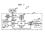
- a solid state audio system 10 which utilizes the present invention capacitive interface 20.
- the audio system 10 includes an audio player 12 operated by means of a digital signal processor (DSP) 14 and having a music chip 16 coupled thereto by means of the capacitive interface 20.
- the music chip 16 is essentially a memory device having digital data stored therein which corresponds to pre-recorded music.
- the pre-recorded audio data is stored in the chip 16 in a compressed format by means of an audio coding algorithm.
- the algorithm reduces the amount of digital information necessary to be stored from a master recording, while still reproducing essentially the same audio quality when the data is read. Encoding by means of the algorithm is necessary in order to store sufficient quantities of data so that the music on the chip may have a time of play comparable to that of current day albums.
- the main hardware architecture of the audio player 12 of FIG. 1 consists of, besides the DSP 14, a stereo coder/decoder (codec) 18, keypad 22, display 24, and associated interface logic in the form of an applications specific integrated circuit (ASIC) 26.
- the audio player 12 is responsible for decoding the encoded bit stream read from the music chip 16 and outputting the music through an output device such as speakers or headphones 28. Parameters of the PAC algorithm are downloaded into external RAM 30 when a chip 16 is loaded into the player 12 in order to assist in the decoding process.
- the audio player 12 includes an address shift register 32 and data shift register 34 which are coupled to the DSP 14 over. associated address and data buses 36, 38.
- the music chip 16 includes an array of memory cells 40, for example, ROM, which are coupled to address and data shift registers 42, 44 via respective address and data buses 46, 48, respectively.
- An address buffer 50 and data buffer 52 are shown interposed between the address shift register 42 and address bus 46 and data shift register 44 and data bus 48 for temporary storage of information.
- the transfer of information between the music chip 16 and audio player 12 can be described as follows. Address information from the audio player 12 is sent out over the address bus 36 where it is received into the address shift register 32 of the audio player 12.
- the address shift register 32 is then adapted to output the address information serially over the interface 20 in accordance with the timing and control signals of the DSP 14 to the corresponding address shift register 42 on the music chip 16.
- the address information is then accessed in parallel form and placed on the address bus 46 where particular memory locations are identified.
- Data is then read from the specified memory location(s) and placed on the data bus 48 where it is received by the data shift register 44.
- the data is then shifted out of the shift register 44 and transferred serially over the interface 20 between the chip and player where it is received by the data shift register 34 of the player 12.
- the information is transferred to the DSP 14 where it is decoded and eventually output as audio. Accordingly, operation of the solid state audio system 10 requires large quantities of data to be transferred at high rates of speed over the data interface 20 between the audio player 12 and music chip 16. Typical data transfer rates range on the order of 150 KHz.
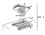
- FIG. 3 there is shown one preferred embodiment of the present invention capacitive interface 20 between the between the music chip 16 and solid state audio player 12.
- An underside view of the chip 16 is shown which depicts a set of four capacitive plates 55-58 for transfer of data between the chip and player. As will be explained two of the capacitive plates are responsible for transfer of data out from the chip while two of the plates receive input data.
- Contacts 60, 61 on either side of the chip are responsible for providing power, ground and clock signals from the audio player to the chip.
- the capacitive plates 55-58 and contacts 60, 61 are essentially flush within the housing of the chip so as to minimize protrusions therefrom.
- the audio player 12 may be a portable or stationary play at home device, and includes one or more receptacle areas 64 which are adapted to receive and hold the music chip 16.
- a set of four capacitive plates 65-68 which correspond to the capacitive plates 55-58 on the music chip are located within the receptacle area 64.
- two plates each on the audio player are adapted to receive data and transfer data.
- Contacts 70, 71 within the receptacle area are also adapted to mate with the contacts 60, 61 located on the sides of the music chip to provide power and clock signals.
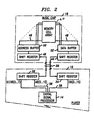
- the output drive circuit 80 is comprised of a combination of driver amplifiers 81, 82, wherein one of the driver amplifiers is inverted from the other.
- the outputs of the driver amplifiers 81, 82 are respectively coupled to capacitive plates 65, 66 located on the exterior of the player.
- the output drive circuit 80 of the audio player receives serial data from the address shift register 32 and differentially drives the capacitive plates 65, 66, which interface with the capacitive plates 55, 56 of the music chip.
- These drivers convert the serial data from the shift register 32 which is of one polarity, into a differential polarity such that for each transition of the data from the shift register, one of the drivers goes positive, while the other goes negative.
- a data receive circuit 84 is also included in the audio player 12 for receiving data transmitted from the music chip 16.
- the data receive circuit 84 is comprised of a differential amplifier 86 and is used in receiving differential data coupled to capacitive plates 67, 68 of the player from capacitive plates 57, 58 of the music chip. This data is then received into the data shift register 34 of the audio player where it is then transmitted to the DSP 14 for appropriate processing.
- Hysterisis is built into the data receive circuit 84 such that a differential pulse greater than the hysterisis is required to switch the output of the amplifier 86 from a high state to a low state or from a low state to a high state.
- the hysterisis aids in preventing outside noise from causing false triggering of the data receive circuit 84 by ignoring small differential noise signals and switching only on larger differential data signals. Accordingly, once the data receive circuit switches states, if there is no further input, it will remain in whatever state it was switched and will not drift back and forth to cause false data indications.
- the music chip 16 includes a data receive circuit 88 and a data output drive circuit 90 for communication with the audio player.
- the data receive circuit 88 is a differential amplifier 93 having inputs coupled to capacitive plates 55, 56 on the music chip. These capacitive plates are capacitively coupled to respective plates 65, 66 on the audio player 12 when the chip 16 is inserted and aligned within the receptacle 64.
- the output of the data receive circuit 88 on the music chip is coupled to the input of the address shift register 42 which receives the serial addressing information and then outputs that information over the address bus 46.
- the output driver circuit 90 of the music chip 16 is comprised of opposed driver amplifiers 91, 92 for differentially driving the respective capacitive plates 57, 58 with the serial data received from the data shift register 44 of the music chip.
- the output capacitive plates 57, 58 on the music chip are coupled to corresponding plates 67, 68 on the audio player 12 which receive the data for processing.
- Two of the capacitive plates are utilized for data input of differential data. while two plates are used for data output.
- the differential data transfer scheme ensures a more reliable transfer of information since two data terminals are active to indicate a transition from one state to another.
- metallic contacts 60, 61 are located on either side of the chip 16 to provide power, ground and clock signals to the internal circuitry thereof.
- metal contacts are provided on the chip, the contacts are mounted closely to the body of the chip so as not to protrude a great distance therefrom. This, in combination with surge protection coupled to the circuit lines running from the contacts, reduces the possibility of damage from ESD.
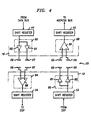
- only two contacts are used to provide power (3.3 VDC), ground and clock signals, wherein the clock signal is transmitted in conjunction with one of the power connections. This is done to reduce susceptibility to ESD by minimizing the exposed contact area, as well as to minimize the effects of corrosion on exposed metal surfaces. Referring to FIG.
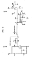
- the dc offset circuit 95 includes transistor T1 (MOSFET) which is biased by means of resistive divider network comprised of resistors R1 and R2 and functions to provide a stable dc offset for the voltage output VDD of the audio player 12.
- the offset signal from the transistor T1 enters a diode-resistive network which prevents bleed-back of the clock signal (OSC) into the power circuit.
- Diode D1 is forward biased to pass the offset signal.
- R3 is assigned a relatively large value, for example, one mega-ohm, so as to be able to pass only minimal feedback current.
- the clock signal (OSC) is added or mixed with the dc offset signal at junction J1 where the clock signal effectively rides on the dc carrier, as shown.
- the dc offset circuit of FIG. 5 also creates a buffer between the power circuitry and the exposed contact.
- the values of R1 and R2 are chosen according to the desired offset, wherein typically, R1 is selected to be much greater than R2.
- the combination signal is transferred from the audio player 12 to the music chip 16 through one of the metal contacts 60. 61, wherein the clock is extracted from the power signal by means of a clock-VDC recovery circuit 96.
- the VDC recovery circuit is comprised of a low pass filter 97 including R11, C11. R11 and C11 integrate the input signal over time to produce a dc signal, wherein VDC appears at the output terminal 98 of the low pass filter 97.
- the clock recovery circuit 99 includes amplifying transistor T2 which is driven into enhancement or depletion mode by the ac clock signal. Capacitor C21 blocks the dc portion of the combination signal and the extracted clock signal appears at an output terminal 100 which is coupled to the drain of transistor T2.
- R11, C11 and RD, RS are chosen so that RD is much greater than RS. It will be understood that in the alternative, three contacts may be provided for the transfer of each of the signals individually. As is known in the art, data transfer is coordinated throughout the music chip 16 and audio player 12 by means of the clock and other corresponding signals which are issued from the DSP.
- a unique interface for transfer of digital data between a semiconductor chip music and associated audio player has thus been presented.
- the interface allows for serial transfer of data to and from the chip by means of a capacitive interface to the audio player, that eliminates the need for metal contacts.
- the interface which utilizes differential data transfer, is extremely reliable and aids in protecting the microelectronics within the chip and audio player from damage caused by handling.
Landscapes
- Signal Processing For Digital Recording And Reproducing (AREA)
- Near-Field Transmission Systems (AREA)
Applications Claiming Priority (2)
| Application Number | Priority Date | Filing Date | Title |
|---|---|---|---|
| US447337 | 1989-12-07 | ||
| US08/447,337 US5694516A (en) | 1995-05-22 | 1995-05-22 | Capacitive interface for coupling between a music chip and audio player |
Publications (3)
| Publication Number | Publication Date |
|---|---|
| EP0744750A2 EP0744750A2 (en) | 1996-11-27 |
| EP0744750A3 EP0744750A3 (en) | 1998-06-10 |
| EP0744750B1 true EP0744750B1 (en) | 2003-03-19 |
Family
ID=23775965
Family Applications (1)
| Application Number | Title | Priority Date | Filing Date |
|---|---|---|---|
| EP96303598A Expired - Lifetime EP0744750B1 (en) | 1995-05-22 | 1996-05-21 | Capacitive interface for coupling between a music chip and audio player |
Country Status (7)
| Country | Link |
|---|---|
| US (1) | US5694516A (enExample) |
| EP (1) | EP0744750B1 (enExample) |
| JP (1) | JPH098712A (enExample) |
| KR (1) | KR960043186A (enExample) |
| CA (1) | CA2176984C (enExample) |
| DE (1) | DE69626717T2 (enExample) |
| TW (1) | TW305969B (enExample) |
Families Citing this family (12)
| Publication number | Priority date | Publication date | Assignee | Title |
|---|---|---|---|---|
| US5648753A (en) * | 1994-11-22 | 1997-07-15 | Martin; Frank A. | Interchangeable sound effect device |
| KR100287366B1 (ko) | 1997-11-24 | 2001-04-16 | 윤순조 | 엠피이지 방식을 이용한 휴대용 음향 재생장치 및 방법 |
| US6425018B1 (en) | 1998-02-27 | 2002-07-23 | Israel Kaganas | Portable music player |
| GB9823356D0 (en) * | 1998-10-27 | 1998-12-23 | Philips Electronics Nv | Data transfer |
| WO2000067258A1 (en) | 1999-04-30 | 2000-11-09 | Thomson Licensing S.A. | Method and apparatus for processing digitally encoded audio data |
| US6824063B1 (en) | 2000-08-04 | 2004-11-30 | Sandisk Corporation | Use of small electronic circuit cards with different interfaces in an electronic system |
| US20030017848A1 (en) * | 2001-07-17 | 2003-01-23 | Engstrom G. Eric | Personalizing electronic devices and smart covering |
| WO2005069585A1 (en) | 2004-01-14 | 2005-07-28 | Innovision Research & Technology Plc | Variable configuration apparatus |
| US20060234405A1 (en) * | 2005-04-13 | 2006-10-19 | Best Scott C | Semiconductor device with self-aligning contactless interface |
| US7450535B2 (en) * | 2005-12-01 | 2008-11-11 | Rambus Inc. | Pulsed signaling multiplexer |
| SI22566A (sl) | 2007-06-21 | 2008-12-31 | Vinko Kunc | Izolirni vmesnik s kapacitivno bariero vsebujočim diferencirnim vezjem in postopek prenosa signalas pomočjo takega izolirnega vmesnika |
| US10310110B2 (en) | 2017-02-21 | 2019-06-04 | Geospace Technologies Corporation | Systems and methods for seismic data acquisition |
Family Cites Families (10)
| Publication number | Priority date | Publication date | Assignee | Title |
|---|---|---|---|---|
| US4717261A (en) * | 1985-01-16 | 1988-01-05 | Casio Computer Co., Ltd. | Recording/reproducing apparatus including synthesized voice converter |
| US4772873A (en) * | 1985-08-30 | 1988-09-20 | Digital Recorders, Inc. | Digital electronic recorder/player |
| DE3545070C2 (de) * | 1985-12-19 | 1995-01-05 | Herbert Wolfram | Herzschrittmacher-Kontrollgerät |
| US4795898A (en) * | 1986-04-28 | 1989-01-03 | American Telephone And Telegraph Company | Personal memory card having a contactless interface using differential data transfer |
| US4798322A (en) * | 1986-04-28 | 1989-01-17 | American Telephone And Telegraph Company | Card reader/writer station for use with a personal memory card using differential data transfer |
| EP0245531A1 (de) * | 1986-05-14 | 1987-11-19 | Deutsche ITT Industries GmbH | Verwendung von halbleitertechnischen Festwertspeichern |
| US4963866A (en) * | 1989-03-27 | 1990-10-16 | Digital Recorders, Inc. | Multi channel digital random access recorder-player |
| JPH03204095A (ja) * | 1989-12-30 | 1991-09-05 | Sony Corp | 情報カード装置 |
| US5119172A (en) * | 1991-03-04 | 1992-06-02 | Motorola, Inc. | Microelectronic device package employing capacitively coupled connections |
| JP3546464B2 (ja) * | 1994-04-04 | 2004-07-28 | 株式会社デンソー | 非接触式icカードのリード/ライト装置 |
-
1995
- 1995-05-22 US US08/447,337 patent/US5694516A/en not_active Expired - Lifetime
-
1996
- 1996-05-21 DE DE69626717T patent/DE69626717T2/de not_active Expired - Lifetime
- 1996-05-21 CA CA002176984A patent/CA2176984C/en not_active Expired - Fee Related
- 1996-05-21 EP EP96303598A patent/EP0744750B1/en not_active Expired - Lifetime
- 1996-05-22 JP JP8126785A patent/JPH098712A/ja active Pending
- 1996-05-22 KR KR1019960017314A patent/KR960043186A/ko not_active Ceased
- 1996-07-06 TW TW085108196A patent/TW305969B/zh not_active IP Right Cessation
Also Published As
| Publication number | Publication date |
|---|---|
| DE69626717T2 (de) | 2004-02-05 |
| DE69626717D1 (de) | 2003-04-24 |
| KR960043186A (ko) | 1996-12-23 |
| JPH098712A (ja) | 1997-01-10 |
| MX9601910A (es) | 1997-07-31 |
| US5694516A (en) | 1997-12-02 |
| EP0744750A3 (en) | 1998-06-10 |
| CA2176984C (en) | 2000-09-19 |
| CA2176984A1 (en) | 1996-11-23 |
| EP0744750A2 (en) | 1996-11-27 |
| TW305969B (enExample) | 1997-05-21 |
Similar Documents
| Publication | Publication Date | Title |
|---|---|---|
| JP3886561B2 (ja) | メモリチップのアーキテクチャ | |
| EP0744750B1 (en) | Capacitive interface for coupling between a music chip and audio player | |
| WO1998055998A3 (en) | Apparatus and method for reproducing a digital audio signal from a record carrier | |
| WO1995035564A3 (en) | Arrangement for recording an information signal on a magnetic record carrier | |
| AU556167B2 (en) | F.m. stereo on video tracks | |
| KR19990072628A (ko) | 오디오재생장치 | |
| CA2074546A1 (en) | Optical magnetic disk recording/reproducing apparatus | |
| MXPA96001910A (en) | Capacitive interconnection for coupling between chip of music and an au player | |
| KR920005465A (ko) | 반도체집적회로 | |
| US4420777A (en) | Tape recorder with cue processor | |
| MXPA96001918A (en) | Memo chip architecture | |
| KR100374816B1 (ko) | 디지털 데이터 플레이어의 데이터 저장매체 검출장치 | |
| US3296385A (en) | Synchronizing system utilizing capacitive coaxial cable pickup for supplying control signal | |
| US5650884A (en) | Magnetic recording and reproducing apparatus having a high-speed changeover | |
| EP0430268B1 (en) | Magnetic recording and playback apparatus | |
| EP0087320A2 (en) | Digital sound storage system | |
| Thompson et al. | Why Dat Matters to Oral Historians | |
| SU1394237A1 (ru) | Устройство дл воспроизведени стереофонического сигнала магнитофона | |
| KR20000035243A (ko) | 활성 헤드 모드 제어 방법 및 장치 | |
| JPS6224406A (ja) | 磁気再生装置 | |
| JPH0495223A (ja) | 光学式情報記録再生装置 | |
| JPH04121802A (ja) | フレキシブルディスク装置 | |
| EP0484929A2 (en) | Audio signal switching circuit | |
| JPH02113403A (ja) | 増幅器の出力インピーダンス制御回路 | |
| JPS60237685A (ja) | デイジタル信号再生方法 |
Legal Events
| Date | Code | Title | Description |
|---|---|---|---|
| PUAI | Public reference made under article 153(3) epc to a published international application that has entered the european phase |
Free format text: ORIGINAL CODE: 0009012 |
|
| AK | Designated contracting states |
Kind code of ref document: A2 Designated state(s): DE GB |
|
| PUAL | Search report despatched |
Free format text: ORIGINAL CODE: 0009013 |
|
| AK | Designated contracting states |
Kind code of ref document: A3 Designated state(s): DE GB |
|
| 17P | Request for examination filed |
Effective date: 19981201 |
|
| 17Q | First examination report despatched |
Effective date: 20000119 |
|
| GRAG | Despatch of communication of intention to grant |
Free format text: ORIGINAL CODE: EPIDOS AGRA |
|
| GRAG | Despatch of communication of intention to grant |
Free format text: ORIGINAL CODE: EPIDOS AGRA |
|
| GRAH | Despatch of communication of intention to grant a patent |
Free format text: ORIGINAL CODE: EPIDOS IGRA |
|
| GRAH | Despatch of communication of intention to grant a patent |
Free format text: ORIGINAL CODE: EPIDOS IGRA |
|
| GRAA | (expected) grant |
Free format text: ORIGINAL CODE: 0009210 |
|
| AK | Designated contracting states |
Designated state(s): DE GB |
|
| REG | Reference to a national code |
Ref country code: GB Ref legal event code: FG4D |
|
| REF | Corresponds to: |
Ref document number: 69626717 Country of ref document: DE Date of ref document: 20030424 Kind code of ref document: P |
|
| PLBE | No opposition filed within time limit |
Free format text: ORIGINAL CODE: 0009261 |
|
| STAA | Information on the status of an ep patent application or granted ep patent |
Free format text: STATUS: NO OPPOSITION FILED WITHIN TIME LIMIT |
|
| 26N | No opposition filed |
Effective date: 20031222 |
|
| PGFP | Annual fee paid to national office [announced via postgrant information from national office to epo] |
Ref country code: GB Payment date: 20140521 Year of fee payment: 19 |
|
| PGFP | Annual fee paid to national office [announced via postgrant information from national office to epo] |
Ref country code: DE Payment date: 20140515 Year of fee payment: 19 |
|
| REG | Reference to a national code |
Ref country code: DE Ref legal event code: R082 Ref document number: 69626717 Country of ref document: DE Representative=s name: DILG HAEUSLER SCHINDELMANN PATENTANWALTSGESELL, DE |
|
| REG | Reference to a national code |
Ref country code: DE Ref legal event code: R119 Ref document number: 69626717 Country of ref document: DE |
|
| GBPC | Gb: european patent ceased through non-payment of renewal fee |
Effective date: 20150521 |
|
| PG25 | Lapsed in a contracting state [announced via postgrant information from national office to epo] |
Ref country code: GB Free format text: LAPSE BECAUSE OF NON-PAYMENT OF DUE FEES Effective date: 20150521 Ref country code: DE Free format text: LAPSE BECAUSE OF NON-PAYMENT OF DUE FEES Effective date: 20151201 |