EP0740418B1 - ODER-Gatter mit kontrollierbarer Breite - Google Patents
ODER-Gatter mit kontrollierbarer Breite Download PDFInfo
- Publication number
- EP0740418B1 EP0740418B1 EP96302889A EP96302889A EP0740418B1 EP 0740418 B1 EP0740418 B1 EP 0740418B1 EP 96302889 A EP96302889 A EP 96302889A EP 96302889 A EP96302889 A EP 96302889A EP 0740418 B1 EP0740418 B1 EP 0740418B1
- Authority
- EP
- European Patent Office
- Prior art keywords
- input
- controllable
- gate
- output
- bit
- Prior art date
- Legal status (The legal status is an assumption and is not a legal conclusion. Google has not performed a legal analysis and makes no representation as to the accuracy of the status listed.)
- Expired - Lifetime
Links
Images

Classifications
-
- H—ELECTRICITY
- H03—ELECTRONIC CIRCUITRY
- H03K—PULSE TECHNIQUE
- H03K19/00—Logic circuits, i.e. having at least two inputs acting on one output; Inverting circuits
- H03K19/02—Logic circuits, i.e. having at least two inputs acting on one output; Inverting circuits using specified components
- H03K19/173—Logic circuits, i.e. having at least two inputs acting on one output; Inverting circuits using specified components using elementary logic circuits as components
- H03K19/1733—Controllable logic circuits
- H03K19/1735—Controllable logic circuits by wiring, e.g. uncommitted logic arrays
- H03K19/1736—Controllable logic circuits by wiring, e.g. uncommitted logic arrays in which the wiring can be modified
-
- G—PHYSICS
- G06—COMPUTING OR CALCULATING; COUNTING
- G06F—ELECTRIC DIGITAL DATA PROCESSING
- G06F5/00—Methods or arrangements for data conversion without changing the order or content of the data handled
- G06F5/01—Methods or arrangements for data conversion without changing the order or content of the data handled for shifting, e.g. justifying, scaling, normalising
- G06F5/012—Methods or arrangements for data conversion without changing the order or content of the data handled for shifting, e.g. justifying, scaling, normalising in floating-point computations
-
- G—PHYSICS
- G06—COMPUTING OR CALCULATING; COUNTING
- G06F—ELECTRIC DIGITAL DATA PROCESSING
- G06F7/00—Methods or arrangements for processing data by operating upon the order or content of the data handled
-
- G—PHYSICS
- G06—COMPUTING OR CALCULATING; COUNTING
- G06F—ELECTRIC DIGITAL DATA PROCESSING
- G06F7/00—Methods or arrangements for processing data by operating upon the order or content of the data handled
- G06F7/38—Methods or arrangements for performing computations using exclusively denominational number representation, e.g. using binary, ternary, decimal representation
- G06F7/48—Methods or arrangements for performing computations using exclusively denominational number representation, e.g. using binary, ternary, decimal representation using non-contact-making devices, e.g. tube, solid state device; using unspecified devices
- G06F7/499—Denomination or exception handling, e.g. rounding or overflow
- G06F7/49942—Significance control
- G06F7/49947—Rounding
- G06F7/49952—Sticky bit
Definitions
- the technical field of this invention is the field of digital data processing and more particularly microprocessor circuits, architectures and methods for digital data processing especially floating point arithmetic.
- Floating point arithmetic often requires alignment of the binary point of two numbers before operation.
- the exponent of the two numbers is compared to determine how much of a shift is needed to align the binary points.
- the mantissa of the smallest number is right shifted a number of places equal to the difference between the exponent of the greatest number and the exponent of the smallest number. This shift aligns the binary points of the number and permits addition or subtraction. The shift also loses some of the least significant bits of the smallest number, which are shifted out.
- the IEEE-754 floating point specification defines four rounding modes: 1) round towards positive infinity; 2) round towards negative infinity; 3) round towards the nearest integer; and 4) round toward zero, also known as truncation.
- the rounding may depend upon whether any of the shifted out least significant bits of the smallest number were 1. This is known as the sticky bit. It is known in the art to view these bits as they are shifted out during the shift operation. This permits detection of whether one or more of these bits is 1. This technique is relatively disadvantageous because it requires the complete shift to take place before the sticky bit is known. It would be advantageous if there were a faster method for determining if one or more of these shifted out least significant bits were 1.
- US 4 864 527 discloses a "sticky bit" circuit having a plurality of stages. Each stage has three inputs: the output of the previous stage, the respective bit of an operand fraction and a control bit indicating whether a right shift of the operand of a respective number of places is required. The first two of those are combined with a NOR gate the output of which is combined with the control bit to form the output of the stage.
- This invention forms a controllable width OR gate.
- Such a controllable width OR gate function is useful in floating point arithmetic.
- the controllable width OR gate employs a plurality of controllable OR gate cells. If the maximum width of the data to be ORed is N bits, then N-1 such controllable OR gate cells are needed.
- controllable width OR gate comprising:
- This invention is a controllable width OR gate. This provides a fast way to program an OR gate from 1 to N bits wide. This function can be useful in floating point arithmetic logic units.
- the controllable width OR gate has two inputs.
- the first input is a data bus of the data to be OR'ed.
- the second input is a control word input used to determine the width of the OR gate.
- the first output is single bit output ORout, which is the OR of all the bits of the data bus regardless of the control word input.
- the second output is a single bit output STout, which is the OR of all the bits of the data bus from bit 0 to the bit specified by the control word.
- the controllable width OR gate is formed of repeated cells. Each of these cells includes the data and control word inputs and forms the ORout and STout outputs.
- the ORout signal from the repeated cells is used as an intermediate signal.
- Figure 1 illustrates a controllable OR gate cell 100 used as a basic building block.
- the controllable OR gate cell 100 has four data inputs, OR0, ST0, OR1 and ST1, a single control input C0, and two outputs: ORout and STout.
- the OR gate 101 forms the OR of the OR0 and OR1 inputs unconditionally.
- the OR gate 101 supplies the ORout output.
- the OR gate 102 forms the OR of the OR0 input and the ST1 input.
- Two pass gates 104 and 105 are controlled in the opposite sense via the signal on control input C0 due to invertor 103. If C0 is "1”, then the output of OR gate 102 is supplied to output STout. If C0 is "0", the ST0 input is supplied to output STout.
- the controllable OR gate cell 100 can be used to form a wide controllable width OR gate.
- a first input D0 supplies both the OR0 and the ST0 inputs and a second input D1 supplies both the OR1 and the ST1 inputs.
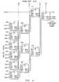
- Figure 2 illustrates a 4 bit wide variable width OR gate employing three controllable OR gate cells.
- Controllable OR gate cells 201, 202 and 203 are constructed as illustrated in Figure 1.
- Data input D0 supplies both the OR0 and the ST0 inputs of controllable OR gate cell 202.
- Data input D1 supplies both the OR1 and the ST1 inputs of controllable OR gate cell 202.
- Data input D2 supplies both the OR0 and the ST0 inputs of controllable OR gate cell 201.
- Data input D3 supplies both the OR1 and the ST1 inputs of controllable OR gate cell 201.
- the control word bit C0 supplies the C0 inputs of both controllable OR gate cells 201 and 202.
- the STout output of controllable OR gate cell 202 supplies the ST0 input of controllable OR gate cell 203.
- the ORout output of controllable OR gate cell 202 supplies the OR0 input of controllable OR gate cell 203.
- the STout output of controllable OR gate cell 201 supplies the ST1 input of controllable OR gate cell 203.
- the ORout output of controllable OR gate cell 201 supplies the OR1 input of controllable OR gate cell 203.
- the control word bit C1 supplies the C0 input of controllable OR gate cells 203.
- the STout output of controllable OR gate cell 203 produces the desired controllable width OR gate output.
- controllable OR gate cell 203 couples only its ST0 input to the OR gate output.
- Controllable OR gate cell 201 supplies the ST0 input of controllable OR gate cell 203 with its ST0 input, which is the D0 input.
- the controllable OR gate output is D0.
- controllable OR gate cell 201 supplies the ST0 input of controllable OR gate cell 203 with an OR of its ST1 input and its OR0 input. This is D0 OR D1.
- the controllable OR gate output is D0 OR D1.
- controllable OR gate cell 203 couples an OR of its ST1 input and its OR0 input the OR gate output.
- the OR0 input of controllable OR gate cell 203 is the ORout of controllable OR gate cell 201, which is D0 OR D1.
- the controllable OR gate output is D0 OR D1 OR D2.
- controllable OR gate cell 203 couples an OR of its ST1 input and its OR0 input the OR gate output.
- the ST1 input of controllable OR gate cell 203 is the STout of controllable OR gate cell 202.
- controllable OR gate cell 203 is the ORout of controllable OR gate cell 201, which is D0 OR D1.
- controllable OR gate output is D0 OR D1 OR D2 OR D3.
- Controllable width OR gates are formed using a plurality of controllable OR gates cell 100.
- a 4 bit wide variable width OR gate is the OR of 2 bit wide variable width OR gates.
- An 8 bit wide variable width OR gate is the OR of two 4 bit wide variable width OR gates, etc.
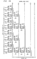
- Figure 3 illustrates the connections of a 32 bit wide variable width OR gate.
- a 32 bit wide variable width OR gate requires 5 control signals C(4:0). As shown in Figure 3, this 32 bit wide OR gate is formed of two 16 bit wide OR gates. If the most significant control bit C4 is "0", then the maximum position up to which it is required to perform the OR is in the lower half of the data bus bits 0 to 15. Therefore the resultant OR from STout is the OR from the least significant 16 bits of the data bus. Which of these bits is controlled by the signals C(3:0). If the most significant control bit C4 is "1", then the maximum position up to which it is required to perform the OR is within the upper half of the data bus bits 16 to 31.
- the resultant OR from STout is all the bits of the least significant half of the data bus D(15:0) OR'ed with the appropriate number of bits of the upper half of the data bus. This number is controlled by the four least significant bits of the control word C(3:0).
- a 32 bit controllable width OR gate is a combination of two 16 bit controllable width OR gates. Similar reasoning applies to a 16 bit controllable width OR gate, a 4 bit controllable width OR gate down to the two bit controllable width OR gate cell 100 of Figure 1.
- Figure 3 illustrates a 32 bit wide controllable width OR gate constructed according to these principles.
- Controllable OR gate cells 301 to 316 directly receive the 32 bits of data D(31:0). Each of these controllable OR gate cells 301 to 316 receives two adjacent bits of the input data. As shown in Figure 3, each data input line drives a ST input and an OR input of the controllable OR gate cell.
- Controllable OR gate cells 301 to 316 are controlled via the C0 bit of the control word C(4:0).
- Controllable OR gate cells 301 to 316 supply signals to controllable OR gate cells 317 to 324.
- controllable OR gate cells 317 to 324 receive an output STout from a first of the controllable OR gate cells 301 to 316 at its ST0 input and an output ORout from this controllable OR gate cell at its OR0 input.
- a second of the controllable OR gate cells 301 to 316 supplies the ST1 and OR1 inputs from its STout output and its ORout, respectively.
- Controllable OR gate cells 317 to 324 are controlled via the C1 bit of the control word C(4:0).
- controllable OR gate cells 325 to 328 receive inputs from the outputs of controllable OR gate cells 317 to 324 and are controlled by the C2 bit of the control word C(4:0).
- Controllable OR gate cells 329 and 330 receive similar inputs from controllable OR gate cells 325 to 328 and are controlled by the C3 bit of the control word C(4:0). Lastly, controllable OR gate cell 331 receives inputs from controllable OR gate cells 329 and 330 and is controlled by the C4 bit of the control word C(4:0). Controllable OR gate cell 331 supplies the 32 bit controllable width OR gate output at its STout output.
- Table 2 shows the relationship between the control word C(4:0), the 32 bits of the date bus D(31:0) and the two outputs Stout and ORout of controllable OR gate cell 331.
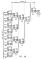
- Figure 4 illustrates how controllable OR gate cells 401 to 412 are connected to construct a 13 bit controllable width OR gate.
- Controllable OR gate cells 401 to 412 are connected in a fashion similar to that shown in Figure 3.
- Figure 4 shows that this technique can be used to form a controllable width OR gate having a size that is not an integral power of 2.
- Table 3 shows the relationship between the control word C(3:0), the 13 bits of the date bus D(13:0) and the two outputs Stout and ORout of controllable OR gate cell 412.
- control word C (3: 0) of (1,1,0,1), (1,1,1,0) and (1,1,1,1), corresponding to OR gate widths of 14, 15 and 16 bits, are defined as the total input width of 13 bits.
- the data input D12 is supplied to both the OR1 and ST1 inputs of controllable OR gate cell 411. This input effectively skips over other controllable OR gate cells which would have been used in a 16 bit wide Controllable width OR gate. Using this skipping technique it is possible to construct controllable width OR gates of any size.
- An N bit wide controllable width OR gate required N-1 controllable OR gate cells such as illustrated in Figure 1.
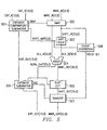
- FIG. 5 Construction of a floating point adder unit employing the controllable width OR gate of this invention as a sticky generator is illustrated in Figure 5. This means a double precision operation can be started on every cycle and has the same latency as single precision.
- the floating point adder unit has the following stages. Exponent comparator/subtractor 501 compares exponents and shift smaller number right to align binary point.
- Swap unit 502 optionally swaps the first and second operands before supply to adder 504.
- Shift right unit 503 receives a signal from exponent comparator/subtractor 501 and makes a corresponding right shift in the second operand. Note that swap unit 502 insures that alignment can be achieved by a right shift.
- the first step in adding or subtracting two binary numbers is to align the mantissa binary points. If exponent comparator/subtractor 501 determines the first operand has the smaller exponent, the two operands are swapped in swap unit 502. The net amount of right shift in the optionally swapped second operand, which now has the smaller exponent, right is the absolute difference between the exponents of the first and second operands. The two operands are then fed into standard full adder 504. Full adder 504 predicts the location of the leading 1 in the mantissa which is used in the normalize step.
- the IEEE standard 754 requires that all operations be done as if using infinite precision and then rounding to the destination format.
- the shift right unit 503 adds 3 bits to the least significant end of the mantissa. The first two are normal extra bits of precision.
- the third bit is the logical OR of all the bits shifted off the end of the mantissa during the right shift of the smallest input number.
- the mantissa After completion of the add/subtract the mantissa is now 3 bits longer than when it started and the hidden bit may not be a "1". This can happen if the two mantissas were subtracted, or the addition of two numbers with opposite signs.
- the definition of a normalized number requires the hidden bit to be a "1".
- the floating point adder unit normalizes the mantissa. Shift left unit 505 left shifts the mantissa until the hidden bit is a "1". The number of shifts required to normalize the mantissa is generated by full adder 504. If the mantissa is shifted left, then exponent subtractor 506 decrements the exponent reflect the new mantissa by subtracting the shift count from the exponent.
- the rounder 507 uses the three extended bits of precision along with the sticky bit, sign, and the rounding mode.
- the rounding modes are defined by the IEEE standard 754 standard and are selected by the user.
- the four rounding modes are 1) round towards positive infinity; 2) round towards negative infinity; 3) round towards the nearest integer; and 4)round toward zero, also known as truncation.
- the round to nearest integer (half adjust) and the round to zero (truncate) are the most common rounding modes.
- the directed rounding modes are normally used to control round off error in a known manner.
- the round to zero mode is simple; the input mantissa is truncated to the destination precision.
- Sticky generator 508 supplies the sticky bit to rounder 507.
- Sticky generator 508 receives the shift amount from exponent comparator/subtractor 501 and the smaller mantissa from swap unit 502.
- Sticky generator 508 consists of a controllable width OR gate of the type described above. The size of the controllable width depends upon the precision selected for the floating point adder.
- the IEEE-744 floating point standard defines single precision as having a mantissa fractional part of 22 bits. Since the right shift may shift out the hidden bit also, the sticky generator for single precision arithmetic should have 23 bits.
- the IEEE-744 floating point standard defines double precision as having a mantissa fractional part of 52 bits. Thus the sticky generator for double precision arithmetic should have 53 bits.
- the floating point unit illustrated in Figure 5 operates upon double precision floating point numbers, note that shift amount has six bits capable of specifying a shift larger than a double precision mantissa.
- the least significant bits of the mantissa received from swap unit 502 serves as the least significant bits of the data supplied to the controllable width OR unit.
- One less than the shift amount serves as the control word for the controllable width OR unit.
- the resultant OR is the sticky bit, which is supplied to rounder 507 for use in the rounding process.
Landscapes
- Engineering & Computer Science (AREA)
- Theoretical Computer Science (AREA)
- Physics & Mathematics (AREA)
- General Engineering & Computer Science (AREA)
- Computing Systems (AREA)
- General Physics & Mathematics (AREA)
- Computer Hardware Design (AREA)
- Mathematical Physics (AREA)
- Logic Circuits (AREA)
Claims (2)
- ODER-Gatter mit steuerbarer Breite, mit:wobei: OR0 das Signal am OR0-Eingang ist, ST0 das Signal am ST0-Eingang ist, OR1 das Signal am OR1-Eingang ist, ST1 das Signal am ST1-Eingang ist, ORout das Signal ist, das am ORout-Ausgang erzeugt wird, STout das Signal ist, das am STout-Ausgang erzeugt wird und C der Steuerbit-Eingang ist;einem Dateneingangsanschluss (D0-D3; D0-D31; D0-D12) mit einer Breite von N Bits;einem Steuerwort-Eingangsanschluss (C0-C1; C0-C4; C0-C3) zum Empfangen eines Steuerworts aus M Bits, wobei M gleich log2N, aufgerundet auf die nächste ganze Zahl von Bits, ist;N - 1 steuerbaren ODER-Gatter-Zellen (100), wovon jede einen OR0-Eingang, einen ST0-Eingang, einen OR1-Eingang, einen ST1-Eingang, einen Steuerbit-Eingang (C0), einen ORout-Ausgang und einen STout-Ausgang besitzt und die folgenden logischen Funktionen ausführt:
ORout = OR0 ODER OR1
STout = [(ST1 ODER OR0) UND C] ODER [ST0 UND NICHT (C)]
einer ersten Schicht (201-202; 301-316; 401-412) der steuerbaren ODER-Gatter-Zellen, wovon jede den OR0- und den ST0-Eingang, die mit demselben entsprechenden Bit des Datenanschlusses verbunden sind, sowie den OR1- und den ST1-Eingang, die beide mit dem nächsthöheren Bit des Dateneingangsanschlusses verbunden sind, aufweist, wobei der Steuerbit-Eingang jeder steuerbaren ODER-Gatter-Zelle der ersten Schicht mit einem niedrigstwertigen Bit (C0) des Steuerwort-Eingangsanschlusses verbunden ist;
wobei die steuerbaren ODER-Gatter-Zellen (203; 317-324; 325-328; 329-330; 331; 407-409; 410-411; 412) nachfolgender Schichten mit ihrem OR0-Eingang jeweils mit dem ORout-Ausgang der ersten steuerbaren ODER-Gatter-Zelle der vorhergehenden Schicht verbunden sind, mit ihrem ST0-Eingang jeweils mit dem STout-Ausgang der ersten steuerbaren ODER-Gatter-Zelle der vorhergehenden Schicht verbunden sind, mit ihrem OR1-Eingang jeweils mit dem ORout-Ausgang einer zweiten steuerbaren ODER-Gatter-Zelle der vorhergehenden Schicht verbunden sind und mit ihrem ST1-Eingang jeweils mit dem STout-Ausgang der zweiten steuerbaren ODER-Gatter-Zelle der vorhergehenden Schicht verbunden sind, wobei die zweite steuerbare ODER-Gatter-Zelle der vorhergehenden Schicht für die erste steuerbare ODER-Gatter-Zelle der vorhergehenden Schicht nächsthöchstwertig ist, wobei die Steuerbit-Eingänge jeder steuerbaren ODER-Gatter-Zelle jeder nachfolgenden Schicht mit einem entsprechenden Bit des Steuerwort-Eingangsanschlusses verbunden sind, wobei jede Schicht, die der ersten Schicht folgt, mit einem nächsthöchstwertigen Bit des Steuerwort-Eingangsanschlusses verbunden ist; und
der STout-Ausgang einer einzelnen steuerbaren ODER-Gatter-Zelle der letzten Schicht den ODER-Gatter-Ausgang mit steuerbarer Breite für eine Anzahl niedrigstwertiger Bits bildet, die dem Steuerwort entsprechen, das bei dem Steuerwort-Eingangsanschluss (C0-C1; C0-C4; C0-C3) empfangen wird. - ODER-Gatter mit steuerbarer Breite nach Anspruch 1, bei dem jede steuerbare ODER-Gatter-Zelle (100) umfasst:ein erstes ODER-Gatter (101), das einen ersten Eingang, der mit dem OR0-Eingang verbunden ist, einen zweiten Eingang, der mit dem OR1-Eingang verbunden ist, und ein Ausgang, der mit dem ORout-Ausgang verbunden ist, umfasst,ein zweites ODER-Gatter (102), das einen ersten Eingang, der mit dem OR0-Eingang verbunden ist, einen zweiten Eingang, der mit dem ST1-Eingang verbunden ist, und einen Ausgang umfasst,ein erstes Durchlassgatter (104), das einen Eingang, der mit dem Ausgang des zweiten ODER-Gatters verbunden ist, einen Ausgang, der mit dem STout-Ausgang verbunden ist, und ein Steuergatter, das mit dem Steuerbit-Eingang verbunden ist, umfasst,einen Inverter (103), der einen Eingang, der mit dem Steuerbit-Eingang verbunden ist, und einen Ausgang umfasst, undein zweites Durchlassgatter (105), das einen Eingang, der mit dem ST0-Eingang verbunden ist, einen Ausgang, der mit dem STout-Ausgang verbunden ist, und ein Steuergatter, das mit dem Ausgang des Inverters verbunden ist, umfasst.
Applications Claiming Priority (2)
| Application Number | Priority Date | Filing Date | Title |
|---|---|---|---|
| US428978 | 1995-04-26 | ||
| US08/428,978 US5502401A (en) | 1995-04-26 | 1995-04-26 | Controllable width or gate |
Publications (2)
| Publication Number | Publication Date |
|---|---|
| EP0740418A1 EP0740418A1 (de) | 1996-10-30 |
| EP0740418B1 true EP0740418B1 (de) | 2004-09-29 |
Family
ID=23701233
Family Applications (1)
| Application Number | Title | Priority Date | Filing Date |
|---|---|---|---|
| EP96302889A Expired - Lifetime EP0740418B1 (de) | 1995-04-26 | 1996-04-25 | ODER-Gatter mit kontrollierbarer Breite |
Country Status (4)
| Country | Link |
|---|---|
| US (1) | US5502401A (de) |
| EP (1) | EP0740418B1 (de) |
| JP (1) | JP3693748B2 (de) |
| DE (1) | DE69633479T2 (de) |
Families Citing this family (3)
| Publication number | Priority date | Publication date | Assignee | Title |
|---|---|---|---|---|
| JP2880958B2 (ja) * | 1996-07-30 | 1999-04-12 | 日本電気アイシーマイコンシステム株式会社 | 半導体集積回路 |
| US8402075B2 (en) * | 2009-03-16 | 2013-03-19 | Advanced Micro Devices, Inc. | Mechanism for fast detection of overshift in a floating point unit of a processing device |
| US10514891B1 (en) * | 2019-05-24 | 2019-12-24 | Google Llc | Multi-input floating-point adder |
Family Cites Families (4)
| Publication number | Priority date | Publication date | Assignee | Title |
|---|---|---|---|---|
| US3912914A (en) * | 1972-12-26 | 1975-10-14 | Bell Telephone Labor Inc | Programmable switching array |
| US5012135A (en) * | 1989-05-12 | 1991-04-30 | Plus Logic, Inc. | Logic gates with a programmable number of inputs |
| US5138198A (en) * | 1991-05-03 | 1992-08-11 | Lattice Semiconductor Corporation | Integrated programmable logic device with control circuit to power down unused sense amplifiers |
| JP3014238B2 (ja) * | 1993-04-28 | 2000-02-28 | 富士通株式会社 | 可変論理演算装置 |
-
1995
- 1995-04-26 US US08/428,978 patent/US5502401A/en not_active Expired - Lifetime
-
1996
- 1996-04-25 EP EP96302889A patent/EP0740418B1/de not_active Expired - Lifetime
- 1996-04-25 DE DE69633479T patent/DE69633479T2/de not_active Expired - Lifetime
- 1996-04-25 JP JP10571096A patent/JP3693748B2/ja not_active Expired - Fee Related
Also Published As
| Publication number | Publication date |
|---|---|
| DE69633479D1 (de) | 2004-11-04 |
| DE69633479T2 (de) | 2005-02-24 |
| EP0740418A1 (de) | 1996-10-30 |
| JP3693748B2 (ja) | 2005-09-07 |
| JPH08335163A (ja) | 1996-12-17 |
| US5502401A (en) | 1996-03-26 |
Similar Documents
| Publication | Publication Date | Title |
|---|---|---|
| US5568412A (en) | Rounding-off method and apparatus of floating point arithmetic apparatus for addition/subtraction | |
| US5357237A (en) | In a data processor a method and apparatus for performing a floating-point comparison operation | |
| US5600583A (en) | Circuit and method for detecting if a sum of two multidigit numbers equals a third multidigit number prior to availability of the sum | |
| US6021424A (en) | Booth multiplier with low power, high performance input circuitry | |
| US4758972A (en) | Precision rounding in a floating point arithmetic unit | |
| US4941120A (en) | Floating point normalization and rounding prediction circuit | |
| US6411980B2 (en) | Data split parallel shifter and parallel adder/subtractor | |
| US6510446B1 (en) | Floating point calculation method and unit efficiently representing floating point data as integer and semiconductor integrated circuit device provided with the same | |
| US4982355A (en) | Low-power parallel multiplier | |
| JPH02294820A (ja) | 浮動小数点数演算処理装置および演算処理方法 | |
| US5771183A (en) | Apparatus and method for computation of sticky bit in a multi-stage shifter used for floating point arithmetic | |
| JPS6131890B2 (de) | ||
| Quach et al. | Design and implementation of the SNAP floating-point adder | |
| EP0740418B1 (de) | ODER-Gatter mit kontrollierbarer Breite | |
| US4349888A (en) | CMOS Static ALU | |
| JPH02178769A (ja) | 浮動小数点データ総和演算回路 | |
| US5754458A (en) | Trailing bit anticipator | |
| US5432727A (en) | Apparatus for computing a sticky bit for a floating point arithmetic unit | |
| US6629119B1 (en) | Arithmetic device and method with low power consumption | |
| JP3137131B2 (ja) | 浮動小数点乗算器及び乗算方法 | |
| EP0356940B1 (de) | Endlicher Automat | |
| US6516333B1 (en) | Sticky bit value predicting circuit | |
| JP3493064B2 (ja) | バレルシフタ | |
| JP2555135B2 (ja) | 演算回路 | |
| US5051943A (en) | Adder circuit with an encoded carry |
Legal Events
| Date | Code | Title | Description |
|---|---|---|---|
| PUAI | Public reference made under article 153(3) epc to a published international application that has entered the european phase |
Free format text: ORIGINAL CODE: 0009012 |
|
| AK | Designated contracting states |
Kind code of ref document: A1 Designated state(s): DE FR GB IT NL |
|
| 17P | Request for examination filed |
Effective date: 19970425 |
|
| 17Q | First examination report despatched |
Effective date: 19991109 |
|
| GRAP | Despatch of communication of intention to grant a patent |
Free format text: ORIGINAL CODE: EPIDOSNIGR1 |
|
| GRAS | Grant fee paid |
Free format text: ORIGINAL CODE: EPIDOSNIGR3 |
|
| GRAA | (expected) grant |
Free format text: ORIGINAL CODE: 0009210 |
|
| AK | Designated contracting states |
Kind code of ref document: B1 Designated state(s): DE FR GB IT NL |
|
| PG25 | Lapsed in a contracting state [announced via postgrant information from national office to epo] |
Ref country code: NL Free format text: LAPSE BECAUSE OF FAILURE TO SUBMIT A TRANSLATION OF THE DESCRIPTION OR TO PAY THE FEE WITHIN THE PRESCRIBED TIME-LIMIT Effective date: 20040929 Ref country code: IT Free format text: LAPSE BECAUSE OF FAILURE TO SUBMIT A TRANSLATION OF THE DESCRIPTION OR TO PAY THE FEE WITHIN THE PRE;WARNING: LAPSES OF ITALIAN PATENTS WITH EFFECTIVE DATE BEFORE 2007 MAY HAVE OCCURRED AT ANY TIME BEFORE 2007. THE CORRECT EFFECTIVE DATE MAY BE DIFFERENT FROM THE ONE RECORDED.SCRIBED TIME-LIMIT Effective date: 20040929 |
|
| REG | Reference to a national code |
Ref country code: GB Ref legal event code: FG4D |
|
| REF | Corresponds to: |
Ref document number: 69633479 Country of ref document: DE Date of ref document: 20041104 Kind code of ref document: P |
|
| NLV1 | Nl: lapsed or annulled due to failure to fulfill the requirements of art. 29p and 29m of the patents act | ||
| ET | Fr: translation filed | ||
| PLBE | No opposition filed within time limit |
Free format text: ORIGINAL CODE: 0009261 |
|
| STAA | Information on the status of an ep patent application or granted ep patent |
Free format text: STATUS: NO OPPOSITION FILED WITHIN TIME LIMIT |
|
| 26N | No opposition filed |
Effective date: 20050630 |
|
| PGFP | Annual fee paid to national office [announced via postgrant information from national office to epo] |
Ref country code: FR Payment date: 20090406 Year of fee payment: 14 |
|
| REG | Reference to a national code |
Ref country code: FR Ref legal event code: ST Effective date: 20101230 |
|
| PGFP | Annual fee paid to national office [announced via postgrant information from national office to epo] |
Ref country code: GB Payment date: 20110328 Year of fee payment: 16 Ref country code: DE Payment date: 20110429 Year of fee payment: 16 |
|
| PG25 | Lapsed in a contracting state [announced via postgrant information from national office to epo] |
Ref country code: FR Free format text: LAPSE BECAUSE OF NON-PAYMENT OF DUE FEES Effective date: 20100430 |
|
| GBPC | Gb: european patent ceased through non-payment of renewal fee |
Effective date: 20120425 |
|
| PG25 | Lapsed in a contracting state [announced via postgrant information from national office to epo] |
Ref country code: GB Free format text: LAPSE BECAUSE OF NON-PAYMENT OF DUE FEES Effective date: 20120425 |
|
| REG | Reference to a national code |
Ref country code: DE Ref legal event code: R119 Ref document number: 69633479 Country of ref document: DE Effective date: 20121101 |
|
| PG25 | Lapsed in a contracting state [announced via postgrant information from national office to epo] |
Ref country code: DE Free format text: LAPSE BECAUSE OF NON-PAYMENT OF DUE FEES Effective date: 20121101 |