EP0738997A2 - A DC-DC converter for a thin film transistor liquid crystal display - Google Patents
A DC-DC converter for a thin film transistor liquid crystal display Download PDFInfo
- Publication number
- EP0738997A2 EP0738997A2 EP96302619A EP96302619A EP0738997A2 EP 0738997 A2 EP0738997 A2 EP 0738997A2 EP 96302619 A EP96302619 A EP 96302619A EP 96302619 A EP96302619 A EP 96302619A EP 0738997 A2 EP0738997 A2 EP 0738997A2
- Authority
- EP
- European Patent Office
- Prior art keywords
- diode
- converter
- tft
- turned
- capacitor
- Prior art date
- Legal status (The legal status is an assumption and is not a legal conclusion. Google has not performed a legal analysis and makes no representation as to the accuracy of the status listed.)
- Ceased
Links
Images


Classifications
-
- H—ELECTRICITY
- H02—GENERATION; CONVERSION OR DISTRIBUTION OF ELECTRIC POWER
- H02M—APPARATUS FOR CONVERSION BETWEEN AC AND AC, BETWEEN AC AND DC, OR BETWEEN DC AND DC, AND FOR USE WITH MAINS OR SIMILAR POWER SUPPLY SYSTEMS; CONVERSION OF DC OR AC INPUT POWER INTO SURGE OUTPUT POWER; CONTROL OR REGULATION THEREOF
- H02M3/00—Conversion of dc power input into dc power output
- H02M3/02—Conversion of dc power input into dc power output without intermediate conversion into ac
- H02M3/04—Conversion of dc power input into dc power output without intermediate conversion into ac by static converters
- H02M3/06—Conversion of dc power input into dc power output without intermediate conversion into ac by static converters using resistors or capacitors, e.g. potential divider
-
- G—PHYSICS
- G09—EDUCATION; CRYPTOGRAPHY; DISPLAY; ADVERTISING; SEALS
- G09G—ARRANGEMENTS OR CIRCUITS FOR CONTROL OF INDICATING DEVICES USING STATIC MEANS TO PRESENT VARIABLE INFORMATION
- G09G3/00—Control arrangements or circuits, of interest only in connection with visual indicators other than cathode-ray tubes
- G09G3/20—Control arrangements or circuits, of interest only in connection with visual indicators other than cathode-ray tubes for presentation of an assembly of a number of characters, e.g. a page, by composing the assembly by combination of individual elements arranged in a matrix no fixed position being assigned to or needed to be assigned to the individual characters or partial characters
- G09G3/2007—Display of intermediate tones
- G09G3/2011—Display of intermediate tones by amplitude modulation
-
- G—PHYSICS
- G09—EDUCATION; CRYPTOGRAPHY; DISPLAY; ADVERTISING; SEALS
- G09G—ARRANGEMENTS OR CIRCUITS FOR CONTROL OF INDICATING DEVICES USING STATIC MEANS TO PRESENT VARIABLE INFORMATION
- G09G3/00—Control arrangements or circuits, of interest only in connection with visual indicators other than cathode-ray tubes
- G09G3/20—Control arrangements or circuits, of interest only in connection with visual indicators other than cathode-ray tubes for presentation of an assembly of a number of characters, e.g. a page, by composing the assembly by combination of individual elements arranged in a matrix no fixed position being assigned to or needed to be assigned to the individual characters or partial characters
- G09G3/34—Control arrangements or circuits, of interest only in connection with visual indicators other than cathode-ray tubes for presentation of an assembly of a number of characters, e.g. a page, by composing the assembly by combination of individual elements arranged in a matrix no fixed position being assigned to or needed to be assigned to the individual characters or partial characters by control of light from an independent source
- G09G3/36—Control arrangements or circuits, of interest only in connection with visual indicators other than cathode-ray tubes for presentation of an assembly of a number of characters, e.g. a page, by composing the assembly by combination of individual elements arranged in a matrix no fixed position being assigned to or needed to be assigned to the individual characters or partial characters by control of light from an independent source using liquid crystals
- G09G3/3611—Control of matrices with row and column drivers
- G09G3/3696—Generation of voltages supplied to electrode drivers
Definitions
- the present invention relates to a direct current-direct current (DC-DC) converter for a thin film transistor liquid crystal display (TFT-LCD), and more particularly, to a low power consumption DC-DC converter which can be used in displaying devices for portable information processing equipment.
- DC-DC direct current-direct current
- Fig. 2 is a detailed circuit diagram of a conventional gray voltage generating circuit. As shown in Fig. 2, a gray voltage is generated from the divided voltage of the resistors and the contrast is marked by applying one of the gray voltages to the liquid crystal capacitor.
- one gray voltage of the plural gray voltages V1 ⁇ V6 is selected with the switches S m , S m+1 , S m+2 to S m+n connected to the source line. Then, once a gate switch Sn connected to the gate line is turned on, the TFTs associated with this gate line are turned on by an applied voltage Von to the gate terminal of the TFTs which are connected to an nth gate line. Once the TFTs of the nth line are turned on, the gray voltage on each source line is applied to the liquid crystal capacitors associated with the S n gate line TFTs and the contrast is displayed on these liquid crystal capacitors.
- the present invention includes first and second switches which are turned on or off in opposition according to a polar signal.
- First and second diodes form electric paths by being turned on when the first and second switches are turned on to thereby charge a first capacitor.
- Third and fourth switches are turned on/off in opposition according to an inverse polar signal.
- Third and fourth diodes form electric paths when the third and fourth switches are turned on to thereby charge a second capacitor.
- a third capacitor is charged by the electric charges of the first and the second capacitors.
- the polar signal and the inverse polar signal have opposite phases.
- PMOS or NMOS type transistors can form the four switches and first and second diodes, and third and fourth diodes may be serially connected in positive direction.
- Plural diodes may be connected to form any one diode.
Abstract
Description
- The present invention relates to a direct current-direct current (DC-DC) converter for a thin film transistor liquid crystal display (TFT-LCD), and more particularly, to a low power consumption DC-DC converter which can be used in displaying devices for portable information processing equipment.
- A conventional DC-DC converter for a TFT-LCD will now be described. Fig. 1, is a graph illustrating a light-transmission ratio of a TFT-LCD. As illustrated in Fig. 1, TFT-LCD contrast increases with voltage because the light transmission ratio changes according to the applied voltage.
- Fig. 2 is a detailed circuit diagram of a conventional gray voltage generating circuit. As shown in Fig. 2, a gray voltage is generated from the divided voltage of the resistors and the contrast is marked by applying one of the gray voltages to the liquid crystal capacitor.
- Fig. 3 is a detailed circuit diagram of a conventional gray voltage generating circuit. As shown in Fig. 3, a conventional TFT-LCD includes a thin film transistor, a liquid crystal capacitor connected between a drain terminal and a common voltage Vcom of the TFT, plural gate lines, and switches connected to each source line and each gate line.
- Operation of the conventional TFT-LCD described above will now be explained. First, one gray voltage of the plural gray voltages V1∼V6 is selected with the switches Sm, Sm+1, Sm+2 to Sm+n connected to the source line. Then, once a gate switch Sn connected to the gate line is turned on, the TFTs associated with this gate line are turned on by an applied voltage Von to the gate terminal of the TFTs which are connected to an nth gate line. Once the TFTs of the nth line are turned on, the gray voltage on each source line is applied to the liquid crystal capacitors associated with the Sn gate line TFTs and the contrast is displayed on these liquid crystal capacitors. Thereafter, after one gray voltage of the gray voltages V1∼V6 is selected with the switches Sm, Sm+1, Sm+2, to Sm+n connected to the respective source lines, the gate switch of the n+1th line is turned on simultaneously as the gate switch of the nth line is turned off, and the power voltage Von is then applied to the gate terminal of the TFTs connected to the n+1th gate line and the TFTs associated with the n_1th gate line are turned on. Once the TFTs of the n+1th line are turned on, the gray voltage on each source line is applied to the associated liquid crystal capacitors via the n+1th gate line TFTs and the contrast is displayed on the liquid crystal display.
- If the above processing is repeated, a desired picture image can be formed wholly by such displayed contrast on the liquid crystal capacitors.
- A typical TFT-LCD is driven by inverting by gate lines, once the nth gate line is selected, one of the gray voltages V1∼V3 is loaded on the source line. Next, when the n+1th gate line is selected, one of the gray voltages V4∼V6 is loaded on the source line. Namely, in driving the line with inversion, as in Fig. 1 illustrating a relation between the voltage and the light-transmission ratio, once the curvilinear points of the relation between the voltage and the light-transmission ratio laid at the right side from Vcom are selected as the liquid crystal capacitor of one line, the curvilinear points of the relation between the voltage and the light-transmission ratio laid at the left side from Vcom are selected as the next liquid crystal capacitor of one line.
- Since a signal which is used as the basis of selecting a polarity of the liquid crystal capacitor, is one of polar signal POL or inverse polar signal POLB as illustrated in Fig. 4, the switches Sm, Sm+1, Sm+2 select one of the gray voltages V1∼V3 or V4∼V6 on the basis of the signals POL, POLB. For instance, one voltage of the gray voltages V1∼V3 is selected when a polar signal POL is at a Vdd level, one voltage of the gray voltages V4∼V6 is selected when the polar signal POL is at a GND level.
- In the gray voltage generating circuit, as illustrated in Fig. 2, a power voltage Vcc is an output power source of the DC-DC converter which is at a voltage level above 8V. The DC-DC converter converts from a Vdd power source of 5V level to a direct current power voltage Vcc of above 8V.
- Fig. 5 is a detailed circuit diagram illustrating a conventional DC-DC converter. As shown in Fig. 5, a conventional DC-DC converter for a TFT-LCD includes a pulse width modulation integrated circuit PWMIC 51 having a power terminal connected to the power source Vdd, a coil L51 having one terminal connected to the power source Vdd, a transistor Q51 having a collector terminal connected to the other terminal of the coil L51, a base terminal connected to an output terminal of the PWMIC 51 and a grounded emitter terminal, a diode D51 having an anode terminal connected to the collector terminal of the transistor Q51 and a capacitor C51 connected between a cathode terminal and a ground of the diode D51.
- Operation of this conventional DC-DC converter for a TFT-LCD will now be described. A PWMIC 51 generates a rectangular pulse and controls a duty ratio, so that a constant DC voltage will be output. If an output DC voltage is above a predetermined value, the duty ratio is reduced, to thereby lower the output DC voltage, and vice versa.
- The transistor Q51 is turned on when the rectangular pulse outputted from the output terminal of the PWMIC 51 is at a high level and the amount of power flowing through the coil L51 is increasing in proportion to the time.
- The amount of the power IL is calculated according to the following equation:

- Next, the transistor Q51 is turned off when the rectangular pulse outputted from the output terminal of the PWMIC 51 is at a low level, thus causing the power flowing through coil L51 to be cut off, and causing a high voltage to turn on the diode D51, so that the power accumulated as a magnetic field on the coil L51 may flow through the diode D51 and charge the capacitor C51. The charged voltage Vcc is used for the power voltage to generate a gray voltage.
- However, the prior DC-DC converter for a TFT-LCD consumes too much power. Although the actual power consumed by the DC-DC converter is only 3mA, the power needed for the electronic circuit, PWMIC, internal resistance of the coil, of the DC-DC converter is more than 20 mA.
- The power conversion efficiency may be expressed according to equation 2:

- An object of the present invention is to solve the problems involved in conventional apparatuses, and to provide a DC-DC converter for a TFT-LCD to be used in portable information processing equipment which itself requires very little power.
- To achieve this object and others, the present invention includes first and second switches which are turned on or off in opposition according to a polar signal. First and second diodes form electric paths by being turned on when the first and second switches are turned on to thereby charge a first capacitor. Third and fourth switches are turned on/off in opposition according to an inverse polar signal. Third and fourth diodes form electric paths when the third and fourth switches are turned on to thereby charge a second capacitor. A third capacitor is charged by the electric charges of the first and the second capacitors.
- Preferably, the polar signal and the inverse polar signal have opposite phases. PMOS or NMOS type transistors can form the four switches and first and second diodes, and third and fourth diodes may be serially connected in positive direction. Plural diodes may be connected to form any one diode.
- The preferred embodiments of the present invention will now be described more specifically with reference to the attached drawings, wherein:
- Fig. 1 is a graph illustrating a liquid crystal light-transmission ratio;
- Fig. 2 is a detailed circuit diagram of a conventional gray voltage generating circuit;
- Fig. 3 is a detailed circuit diagram of a conventional TFT-LCD;
- Fig. 4 is a wave form for an inverse driving of a typical TFT-LCD;
- Fig. 5 is a detailed circuit diagram of a conventional TFT-LCD;
- Fig. 6 is a detailed circuit diagram of a DC-DC converter for TFT-LCD according to a preferred embodiment of the present invention; and
- Fig. 7 is a wave form illustrating each sectional operation of a DC-DC converter for a TFT-LCD according to a preferred embodiment of this invention.
- A preferred embodiment will now be described with particular reference to Figs. 6 and 7.
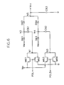
- As shown in Fig. 6, a DC-DC converter for a TFT-LCD according to a preferred embodiment of this invention includes transistors M61, M62 having their source terminals connected to a power signal line Vdd and a ground signal line GND, respectively, and their gate terminals connected in common to a polar signal line POL. The converter also includes transistors M63, M64 having their source terminals connected to the power signal line Vdd and the grounded signal line GND, respectively, and their gate terminal jointly connected to a inverse polar signal line POLB.
- Diodes D61 and D63 are provided, the anodes of which are connected to power signal line Vdd. Diodes D62 and D64 have their anode terminals connected to the cathode terminals of diodes D61 and D63, respectively. The cathode terminals of the diodes D62 and D64 are connected together, and a capacitor is connected between the cathode terminals of the diodes D62, D64 and ground.
- In the preferred embodiment of the invention, the diodes D61, D62, D63, and D64 are used in pairs with each signal POL or POLB, however plural diodes can be used instead of only two diodes.
- Operation of the TFT-LCD according to the preferred embodiment of the invention is described below.
- As illustrated in Fig. 7, when the signal POL has a ground potential, the power signal Vdd is applied to a Node N1 by turning on the PMOS type transistor M61. When the POL is at a power level, the ground level signal is applied to a node N1 by turning on the NMOS type transistor M62. Accordingly, a pulse wave form signal is generated in the node N1 according to the POL signal as illustrated in Fig. 7.
- When the node N1 is at a ground level, the electrons applied through the diode D61 are charged to the capacitor C61. The amount of charge accumulated by the capacitor C61 is calculated according to equation 3 below:

- When the node N1 is at a power level Vdd, the potential of the node N2 is (Vdd + Q61/C61), which may be combined with equation 3 to get (2Vdd - Vd). In this case the diode D61 is turned off from the applied reverse-bias, and the electrons at node N2 are transferred to the capacitor C63 by turning on the diode D62.
- The amount of the electrons Q63 charged to the capacitor C63 flows though the diode D62 until the diode D62 is turned off, and is calculated according to equation 4 below.

- As illustrated in Fig. 7, when the inverse polar signal POLB is at a ground level, the PMOS type transistor M63 is turned on and a power signal Vdd is applied to the node N3. When the inverse polar signal POLB is at a power level Vdd, the NMOS type transistor M64 is turned on and the ground level signal is applied to the node N3. Accordingly, a pulse wave form signal as in Fig. 7 is generated to the node N3 in accordance to the inverse polar signal POLB.
- When the node is at a ground level, the electrons applied through the diode D63 are charged to the capacitor C62, the amount of electron Q62 charged to the capacitor C62 is calculated as the equation 5 below.

- When the node N3 is at a power level Vdd, a potential of the node N4 is (Vdd + Q62/C62) and results in (2Vdd - Vd) with the equation 5. In this case the diode D63 is turned off from the applied reverse-bias, and the electron of the node N4 is charged to the capacitor C63 by the turn on of the diode D64.
- The charge Q63 applied to the capacitor C63 flows though the diode D64 until the diode D64 is turned off, and is calculated as the equation 6 below.

- The polar signal POL and the inverse polar signal POLB are of opposite phase. Therefore, generalizing the whole operation, a constant direct current voltage Vcc equal to 2(Vdd - Vd), is outputted to the node N5 as illustrated in Fig. 7. Accordingly, the small power consuming DC-DC converter can be provided by supplying a stabilized direct current voltage Vcc using MOS transistors M61 to M64 and diodes D61 to D64 which consume low amounts of power. If a number of the diodes D611 to D64 is controlled, the value of the direct current voltage Vcc can be randomly set.
- The preferred embodiment of the invention provides a DC-DC converter for a TFT-LCD which may be used in portable information processing equipment because the DC-DC converter consumes very little power.
- It is understood that various other modifications will be apparent to and can be readily made by those skilled in the art without departing from the scope and spirit of this invention. Accordingly, it is not intended that the scope of the claims appended hereto be limited to the description as set forth herein, but rather that the claims be construed as encompassing all the features of patentable novelty that reside in the present invention, including all features that would be treated as equivalents thereof by those skilled in the art which this invention pertains.
Claims (5)
- A DC-DC converter for a TFT-LCD, comprising:a first switch and a second switch which are turned on and off in opposition according to a polar signal;a first diode and a second diode which form electric paths by being turned on when the first and the second switches are turned on;a first capacitor which charges when the electric paths of the first and the second diodes are formed;a third diode and a fourth diode which form electric paths by being turned on when the third and the forth switches are turned on;a second capacitor which charges when the electric paths of the third and the fourth diodes are formed; anda third capacitor which is charged by the electric charges of the first and the second capacitors.
- A DC-DC converter for a TFT-LCD as claimed in Claim 1, wherein said polar signal and the inverse polar signal have opposite phases.
- A DC-DC converter for a TFT-LCD as claimed in Claim 1 or Claim 2, wherein said first switch and second switch, said third switch and said fourth switch each use a PMOS or NMOS type transistor.
- A DC-DC converter for a TFT-LCD as claimed in any of Claims 1 to 3, wherein said first diode and second diode, and said third diode and said fourth diode are respectively serially connected in a positive direction.
- A DC-DC converter for a TFT-LCD, comprising:a switch circuit which inputs a pulsed polar signal and an inverse polar pulse signal and outputs a first pulsed voltage to a first node and a second pulsed voltage to a second node;a charge circuit connected between said first and second nodes and an output node, said charge circuit further connected to a power source having a power source voltage such that third and forth nodes within said charging circuit are intermittently raised by a capacitor to a charging voltage level which exceeds said power source voltage; said third and fourth nodes each connected through a diode to said output node; anda smoothing capacitor connected to said output node.
Applications Claiming Priority (2)
| Application Number | Priority Date | Filing Date | Title |
|---|---|---|---|
| KR1019950009107A KR0139664B1 (en) | 1995-04-18 | 1995-04-18 | Dc-dc converter for liquid crystal display equipment using the thin film transistor |
| KR9509107 | 1995-04-18 |
Publications (2)
| Publication Number | Publication Date |
|---|---|
| EP0738997A2 true EP0738997A2 (en) | 1996-10-23 |
| EP0738997A3 EP0738997A3 (en) | 1997-02-05 |
Family
ID=19412437
Family Applications (1)
| Application Number | Title | Priority Date | Filing Date |
|---|---|---|---|
| EP96302619A Ceased EP0738997A3 (en) | 1995-04-18 | 1996-04-15 | A DC-DC converter for a thin film transistor liquid crystal display |
Country Status (5)
| Country | Link |
|---|---|
| US (1) | US5712778A (en) |
| EP (1) | EP0738997A3 (en) |
| JP (1) | JPH08289533A (en) |
| KR (1) | KR0139664B1 (en) |
| TW (1) | TW301077B (en) |
Cited By (1)
| Publication number | Priority date | Publication date | Assignee | Title |
|---|---|---|---|---|
| EP1176580A3 (en) * | 2000-07-28 | 2002-11-06 | Lg Electronics Inc. | Driving circuit for organic electroluminescence device |
Families Citing this family (22)
| Publication number | Priority date | Publication date | Assignee | Title |
|---|---|---|---|---|
| KR100455651B1 (en) * | 1997-08-08 | 2005-01-17 | 삼성전자주식회사 | Multi-output dc/dc voltage converting apparatus and liquid crystal display, including multi-output dc/dc voltage converter for generating main power through choke system and auxiliary power through flyback system |
| US6188265B1 (en) * | 1997-12-12 | 2001-02-13 | Scenix Semiconduction, Inc. | High-voltage NMOS switch |
| KR100590748B1 (en) * | 1998-12-04 | 2006-09-18 | 삼성전자주식회사 | Low voltage input voltage compensation circuit of thin film transistor liquid crystal display driving circuit |
| KR20010061843A (en) * | 1999-12-29 | 2001-07-07 | 박종섭 | Dc-dc converter using polar signal in liquid crystal display |
| US20050024125A1 (en) * | 2003-08-01 | 2005-02-03 | Mcnitt John L. | Highly efficient, high current drive, multi-phase voltage multiplier |
| JP4417693B2 (en) * | 2003-11-12 | 2010-02-17 | 東芝モバイルディスプレイ株式会社 | DC-DC conversion circuit |
| TWI261407B (en) * | 2004-08-03 | 2006-09-01 | Ememory Technology Inc | Charge pump circuit |
| CN100345034C (en) * | 2004-09-08 | 2007-10-24 | 友达光电股份有限公司 | Plane display panel of built-in DC-DC converter |
| US20070279350A1 (en) * | 2006-06-02 | 2007-12-06 | Kent Displays Incorporated | Method and apparatus for driving bistable liquid crystal display |
| US7675239B2 (en) * | 2006-08-11 | 2010-03-09 | Kent Displays Incorporated | Power management method and device for low-power displays |
| US7917747B2 (en) * | 2007-03-22 | 2011-03-29 | Igt | Multi-party encryption systems and methods |
| GB2447957A (en) * | 2007-03-30 | 2008-10-01 | Sharp Kk | DC-DC converter arrangement for a display driver and display |
| TW200919959A (en) * | 2007-10-31 | 2009-05-01 | Au Optronics Corp | Charge pump system and method of operating the same |
| US8339185B2 (en) | 2010-12-20 | 2012-12-25 | Sandisk 3D Llc | Charge pump system that dynamically selects number of active stages |
| US9077238B2 (en) | 2013-06-25 | 2015-07-07 | SanDisk Technologies, Inc. | Capacitive regulation of charge pumps without refresh operation interruption |
| US9083231B2 (en) * | 2013-09-30 | 2015-07-14 | Sandisk Technologies Inc. | Amplitude modulation for pass gate to improve charge pump efficiency |
| US9154027B2 (en) | 2013-12-09 | 2015-10-06 | Sandisk Technologies Inc. | Dynamic load matching charge pump for reduced current consumption |
| JP6515570B2 (en) * | 2015-02-18 | 2019-05-22 | Tdk株式会社 | Control circuit and switching power supply |
| US9917507B2 (en) | 2015-05-28 | 2018-03-13 | Sandisk Technologies Llc | Dynamic clock period modulation scheme for variable charge pump load currents |
| US9647536B2 (en) | 2015-07-28 | 2017-05-09 | Sandisk Technologies Llc | High voltage generation using low voltage devices |
| US9520776B1 (en) | 2015-09-18 | 2016-12-13 | Sandisk Technologies Llc | Selective body bias for charge pump transfer switches |
| CN114596823B (en) * | 2020-12-07 | 2023-04-25 | 华润微集成电路(无锡)有限公司 | LCD driving circuit structure for realizing low power consumption and wide working voltage |
Citations (3)
| Publication number | Priority date | Publication date | Assignee | Title |
|---|---|---|---|---|
| US3818484A (en) * | 1971-12-29 | 1974-06-18 | Sharp Kk | Power supply circuit for electronic digital system |
| GB2078021A (en) * | 1980-06-13 | 1981-12-23 | Hitachi Ltd | Power supply circuits |
| US5036229A (en) * | 1989-07-18 | 1991-07-30 | Gazelle Microcircuits, Inc. | Low ripple bias voltage generator |
Family Cites Families (8)
| Publication number | Priority date | Publication date | Assignee | Title |
|---|---|---|---|---|
| US4807104A (en) * | 1988-04-15 | 1989-02-21 | Motorola, Inc. | Voltage multiplying and inverting charge pump |
| JPH02146955A (en) * | 1988-08-30 | 1990-06-06 | Michiko Naito | Electrostatic transformer |
| GB2245112A (en) * | 1990-06-13 | 1991-12-18 | Philips Electronic Associated | Dc/dc voltage multiplier. |
| US5132895A (en) * | 1990-12-11 | 1992-07-21 | Motorola, Inc. | Variable charge pumping DC-to-DC converter |
| JPH05268763A (en) * | 1992-03-17 | 1993-10-15 | Nec Corp | Dc/dc converter circuit and rs-232 interface circuit employing same |
| JP2828881B2 (en) * | 1993-10-04 | 1998-11-25 | 沖電気工業株式会社 | High voltage power circuit |
| JP3282915B2 (en) * | 1994-03-31 | 2002-05-20 | 富士通株式会社 | DC / DC converter and method of controlling back gate voltage of NMOS transistor |
| US5563779A (en) * | 1994-12-05 | 1996-10-08 | Motorola, Inc. | Method and apparatus for a regulated supply on an integrated circuit |
-
1995
- 1995-04-18 KR KR1019950009107A patent/KR0139664B1/en not_active IP Right Cessation
- 1995-11-10 JP JP7292942A patent/JPH08289533A/en active Pending
-
1996
- 1996-04-15 TW TW085104476A patent/TW301077B/zh not_active IP Right Cessation
- 1996-04-15 EP EP96302619A patent/EP0738997A3/en not_active Ceased
- 1996-04-16 US US08/633,288 patent/US5712778A/en not_active Expired - Lifetime
Patent Citations (3)
| Publication number | Priority date | Publication date | Assignee | Title |
|---|---|---|---|---|
| US3818484A (en) * | 1971-12-29 | 1974-06-18 | Sharp Kk | Power supply circuit for electronic digital system |
| GB2078021A (en) * | 1980-06-13 | 1981-12-23 | Hitachi Ltd | Power supply circuits |
| US5036229A (en) * | 1989-07-18 | 1991-07-30 | Gazelle Microcircuits, Inc. | Low ripple bias voltage generator |
Cited By (2)
| Publication number | Priority date | Publication date | Assignee | Title |
|---|---|---|---|---|
| EP1176580A3 (en) * | 2000-07-28 | 2002-11-06 | Lg Electronics Inc. | Driving circuit for organic electroluminescence device |
| CN100397456C (en) * | 2000-07-28 | 2008-06-25 | Lg电子株式会社 | Driving circuit used for organic electroluminescent device |
Also Published As
| Publication number | Publication date |
|---|---|
| KR960039567A (en) | 1996-11-25 |
| EP0738997A3 (en) | 1997-02-05 |
| US5712778A (en) | 1998-01-27 |
| KR0139664B1 (en) | 1998-08-17 |
| TW301077B (en) | 1997-03-21 |
| JPH08289533A (en) | 1996-11-01 |
Similar Documents
| Publication | Publication Date | Title |
|---|---|---|
| US5712778A (en) | Voltage multiplying DC-DC converter for a thin film transistor liquid crystal display | |
| US5635776A (en) | Charge pump voltage converter | |
| US8665255B2 (en) | Power supply circuit and display device including the same | |
| JP3693464B2 (en) | Display panel drive device | |
| EP1553554A3 (en) | Reference voltage generation circuit, display drive circuit, and display device | |
| US20050184946A1 (en) | Pulse compensator, display device and method of driving the display device | |
| KR20070092153A (en) | Charge pump type switching power apparatus | |
| KR0166110B1 (en) | Drive voltage generating device for liquid crystal display device | |
| US7005912B2 (en) | Simple step-up apparatus including level shift circuits capable of low breakdown voltage | |
| JP2004096716A (en) | Level shifter and flat display device | |
| US6188395B1 (en) | Power source circuit, power source for driving a liquid crystal display, and a liquid crystal display device | |
| US20110175892A1 (en) | Power source circuit and liquid crystal display apparatus having the same | |
| JP2008148514A (en) | Dcdc converter | |
| KR101262785B1 (en) | Liquid crystal display and method of driving the same | |
| EP0766371B1 (en) | Small DC power supply | |
| US6861889B2 (en) | Amplitude converting circuit | |
| KR860002877A (en) | Integrated circuit for operation and display control | |
| EP3001554A1 (en) | Fractional output voltage multiplier | |
| US6084580A (en) | Voltage generating circuit and liquid crystal display device incorporating the voltage generating circuit | |
| US6144357A (en) | Driving voltage generating circuit voltage for liquid crystal display | |
| TW200527367A (en) | DC-DC conversion circuit | |
| JP4357698B2 (en) | Reset circuit and power supply device | |
| US6867755B2 (en) | Device and method for driving EL device | |
| JPH0923639A (en) | Voltage converter | |
| JP2006209295A (en) | Power supply device |
Legal Events
| Date | Code | Title | Description |
|---|---|---|---|
| PUAI | Public reference made under article 153(3) epc to a published international application that has entered the european phase |
Free format text: ORIGINAL CODE: 0009012 |
|
| AK | Designated contracting states |
Kind code of ref document: A2 Designated state(s): DE FR GB NL |
|
| PUAL | Search report despatched |
Free format text: ORIGINAL CODE: 0009013 |
|
| AK | Designated contracting states |
Kind code of ref document: A3 Designated state(s): DE FR GB NL |
|
| 17P | Request for examination filed |
Effective date: 19970628 |
|
| 17Q | First examination report despatched |
Effective date: 20000225 |
|
| STAA | Information on the status of an ep patent application or granted ep patent |
Free format text: STATUS: THE APPLICATION HAS BEEN REFUSED |
|
| 18R | Application refused |
Effective date: 20020503 |