EP0736951A2 - Circuit et procédé de détection et d'indication de l'état de charge d'une cellule ou d'une batterie - Google Patents
Circuit et procédé de détection et d'indication de l'état de charge d'une cellule ou d'une batterie Download PDFInfo
- Publication number
- EP0736951A2 EP0736951A2 EP96302399A EP96302399A EP0736951A2 EP 0736951 A2 EP0736951 A2 EP 0736951A2 EP 96302399 A EP96302399 A EP 96302399A EP 96302399 A EP96302399 A EP 96302399A EP 0736951 A2 EP0736951 A2 EP 0736951A2
- Authority
- EP
- European Patent Office
- Prior art keywords
- charge
- signal
- voltage
- cell
- circuit
- Prior art date
- Legal status (The legal status is an assumption and is not a legal conclusion. Google has not performed a legal analysis and makes no representation as to the accuracy of the status listed.)
- Withdrawn
Links
Images


Classifications
-
- H—ELECTRICITY
- H02—GENERATION; CONVERSION OR DISTRIBUTION OF ELECTRIC POWER
- H02J—CIRCUIT ARRANGEMENTS OR SYSTEMS FOR SUPPLYING OR DISTRIBUTING ELECTRIC POWER; SYSTEMS FOR STORING ELECTRIC ENERGY
- H02J7/00—Circuit arrangements for charging or depolarising batteries or for supplying loads from batteries
- H02J7/007—Regulation of charging or discharging current or voltage
- H02J7/00712—Regulation of charging or discharging current or voltage the cycle being controlled or terminated in response to electric parameters
- H02J7/00714—Regulation of charging or discharging current or voltage the cycle being controlled or terminated in response to electric parameters in response to battery charging or discharging current
-
- Y—GENERAL TAGGING OF NEW TECHNOLOGICAL DEVELOPMENTS; GENERAL TAGGING OF CROSS-SECTIONAL TECHNOLOGIES SPANNING OVER SEVERAL SECTIONS OF THE IPC; TECHNICAL SUBJECTS COVERED BY FORMER USPC CROSS-REFERENCE ART COLLECTIONS [XRACs] AND DIGESTS
- Y10—TECHNICAL SUBJECTS COVERED BY FORMER USPC
- Y10S—TECHNICAL SUBJECTS COVERED BY FORMER USPC CROSS-REFERENCE ART COLLECTIONS [XRACs] AND DIGESTS
- Y10S320/00—Electricity: battery or capacitor charging or discharging
- Y10S320/18—Indicator or display
- Y10S320/21—State of charge of battery
Definitions
- This invention relates generally to battery or electrochemical cell charge status detectors and indicators, and corresponding methods, and more particularly to circuits and methods for detecting and indicating the state of charge of individual or multiple electrochemical cells or batteries.
- Battery chargers for nickel cadmium batteries have been used for many years. In past they were generally characterized in having relatively simple circuits for terminating the provision of charging current to a battery. In one such common circuit, as soon as a battery's voltage equaled or exceeded the voltage provided by a full wave bridge rectifier, the provision of charging current to the battery was terminated.
- the state of charge of a battery was determined by monitoring changes in battery voltage or temperature, or by measuring the average value of charge current provided to the battery. Yet other prior art circuits terminated battery charging when a certain predetermined amount of time had passed, or when a certain number of current pulses provided to the charging battery had been missed over a predetermined period of time.
- Nickel cadmium and nickel metal hydride batteries have relatively low internal impedances, usually on the order of about 50 milliohms. Thus, open-circuit voltages (OCVs) and closed circuit voltages (CCVs) measured in those types of batteries do not differ significantly. As such a nickel-cadmium or nickel metal hydride battery nears the end of the charge cycle, voltage typically rises, levels off, and finally decreases. This decrease in battery voltage during the charge cycle is often used to terminate the charge cycle.
- Still other prior art charging circuits continuously measured the average amount of charging current provided to a battery, and terminated charging when the average amount of current fell below a certain minimum threshold value.
- Rechargeable alkaline batteries have an intemal impedance as high as 5 ohms, which is much higher than the internal impedance characteristic of nickel cadmium or nickel metal hydride batteries.
- the relatively high internal impedance of rechargeable alkaline batteries presented significant problems respecting the accurate measurement of battery voltage.
- OCV open-circuit voltage
- the open-circuit voltage (OCV) of rechargeable alkaline batteries was typically measured between charging pulses for an accurate indication of the battery's state of charge. See, for example, U.S. Patent No. 4,977,364 to Kordesch et al., the disclosure of which is hereby incorporated by reference in its entirety, wherein the technique of "IR-free" charging of rechargeable alkaline manganese dioxide cells is described.
- state of charge may be determined accurately using a closed circuit voltage (CCV) measurement obtained during charging.
- the charge status detector of the invention has certain objects. That is, the invention provides solutions to problems existing in the prior art. For example, the invention provides a circuit for detecting the state of charge of a rechargeable cell that: (a) is safe and reliable; (b) is relatively inexpensive; (c) has few electronic components; (d) is easy to implement, and (e) does not directly measure the temperature, the CCV, the OCV, or the level of current provided to a cell.
- the charge status detector of the invention monitors a charge signal, determines a time-averaged value corresponding to the time-averaged charge signal, and detects whether the state of charge of the cell is above a predetermined level by comparing the time-averaged value to a predetermined reference value.
- the charge signal can be a charge enable control signal, a transistor base drive signal, or a signal from a current transformer.
- the charge status detector of the invention has two preferred features: (a) a low-pass filter in combination with a comparator, and (b) a microprocessor, digital signal processor, or other software programmable device.
- a charge enable control or a transistor base drive signal is applied to a charge status detector circuit comprising a low-pass filter network and a comparator.
- a capacitor in the low-pass filter network charges up or discharges through a resistor, depending on whether the open-circuit voltage of the cell being charged is greater or less than the voltage of the capacitor.
- the low-pass filter produces an output signal which is provided as a first input to a comparator.
- the comparator receives a reference voltage signal as a second input. According to the relative amplitudes of the first and second inputs, the comparator produces an output signal corresponding to the state of charge of a rechargeable cell.
- the output signal of the comparator turns a visual indicator, or a circuit for driving a visual indicator, ON or OFF.
- a charge enable control or a transistor base drive signal is applied to a charge status detector circuit comprising a microprocessor, digital signal processor, or other software programmable device.
- the microprocessor determines a time-averaged value corresponding to the time-averaged charge enable control or transistor base drive signal, and compares it to a predetermined reference value. According to the sign and magnitude of the difference between the time-averaged value and the predetermined reference value, the microprocessor produces an output signal corresponding to the state of charge of a rechargeable cell.
- the output signal of the microprocessor turns a visual indicator, or a circuit for driving a visual indicator, ON or OFF.
- the invention possesses certain advantages, including its simplicity, the low cost of the components required to make it, and the small number of modifications required to known charging circuits to implement it Other objects, features, and advantages of the invention will become apparent from the detailed description of the invention.
- cell electrochemical cell
- battery battery
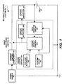
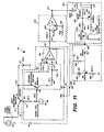
- Figure 1 shows a block diagram of a battery charging system 20 including a charge status detector 120.
- the block diagram of Figure 1 illustrates a pulse-modulated, voltage-controlled battery charging system of a type used for charging rechargeable alkaline manganese dioxide cells.
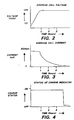
- Figures 2 and 3 show, respectively, the average cell voltage and current signals obtained using battery charging system 20.
- Figure 4 shows the output signal provided by charge status indicator 120 of Figure 1, and corresponds to the signals shown in Figures 2 and 3.
- the voltage across cell 30 rises rapidly during the initial portion of the charging cycle, but remains substantially constant thereafter.
- the portion of the voltage versus time curve of Figure 2 where voltage remains substantially constant represents a significant portion of the charge cycle.
- the state of charge of cell 30 corresponding to the constant voltage portion of the charge cycle may therefore range anywhere between 50% and 100% of full capacity.
- the amplitude of the average charge current provided to cell 30 is much higher during the initial portion of the charge cycle than it is during the remainder of the charge cycle. As the state of charge of cell 30 increases to higher levels, the average current cell 30 accepts decreases.
- the amplitude of the initial charge current provided by the battery charging system 20 to the cell 30 may be determined by the current delivering capacity of the system 20, or by the characteristics of cell 30 charged therein.
- Rechargeable alkaline manganese dioxide cells generally accept charge at a high rate initially, but cannot do so on a continuous basis. Moreover, accurate measurement of the voltage of a rechargeable alkaline manganese dioxide cell cannot be obtained by measuring the CCV of the cell during charging. Instead, only the OCV of a rechargeable alkaline manganese dioxide cell provides an accurate measurement of cell voltage during charging.
- Pulse-modulated battery charging system 20 monitors the OCV of cell 30 during charging and provides charge pulses thereto. As the charge cycle continues, charging current provided to cell 30 is progressively decreased through reducing the pulse duty cycle, or by progressively skipping an increasing number of charge pulses. Thus, progressively less current is provided to cell 30 as the charge cycle continues. As shown in Figure 3, at the end of the charge cycle the average current provided to cell 30 approximates zero; at this point in the charge cycle cell 30 has attained a full state of charge.
- FIG 1 shows the basic components of charging system 20, comprising power source 40, first electronic switch 50, and control circuit 60.
- Current limiting circuit or component 70 may optionally be included in the system, depending on the specific requirements and characteristics of cell 30 and battery charging system 20.
- the primary components of control circuit 60 are voltage reference 80, system clock 90, charge enable control circuit 100, cell monitor circuit 110, and charge status detector 120.
- Control circuit 60 provides battery charging system 20 with the ability to charge cell 30 in accordance with the charge and indication profiles shown in Figures 2, 3, and 4.
- first electronic switch 50 operates at the maximum frequency or duty cycle set by system clock 90.
- a maximum charge current determined by the combination of current limiting circuit or component 70 and the output capacity of power source 40, is provided to cell 30 during the initial portion of the charge cycle.
- System clock 90 also operates to activate and deactivate cell monitor circuit 110 such that the OCV of cell 30 may be sensed when first electronic switch 50 is open (e.g., when current pulses are not being provided to cell 30).
- Charge enable control circuit 100 receives signals corresponding to (a) the OCV of cell 30 from cell monitor circuit 110, and (b) a reference voltage (V ref ) provided by voltage reference 80. Charge enable control circuit 100 compares the OCV to V ref , and then determines whether cell 30 should receive another charge pulse. If the OCV is greater than or equal to V ref , charge enable control circuit 100 disables the provision of a charge pulse to cell 30 for the following clock pulse. Charge enable control circuit 100 does not permit first electronic switch 50 to dose unless and until the OCV of cell 30 falls below V ref .
- the charge enable control signal comprises a series of fixed amplitude pulses having a variable duty cycle.
- the effective duty cycle decreases as cell 30 reaches a full state of charge.
- the time-averaged voltage corresponding to the charge enable control signal varies slowly respecting time, and may thus be described as a quasi-DC equivalent, or low-pass filtered equivalent, of the charge enable control signal.
- the time-averaged, quasi-DC equivalent, or low-pass filtered signal is compared to a reference voltage signal (V min ).
- V min a reference voltage signal
- the output of the comparator changes state. This change in state is used to indicate that cell 30 has attained a full state of charge.
- a microprocessor determines a time-averaged value corresponding to the time-averaged charge enable control signal.
- the microprocessor compares the time-averaged value to a predetermined reference value. When the time-averaged value is less than the predetermined reference value, an output signal from the microprocessor changes state. This change in state is used to indicate that cell 30 has attained a full state of charge.
- the charge status detector of the invention monitors a charge signal, determines a time-averaged value corresponding to the time-averaged charge signal, and detects whether the state of charge of the cell is above a predetermined level by comparing the time-averaged value to a predetermined reference value.
- the charge signal can be any one of a charge enable control signal, a transistor base drive signal, or a signal from a current transformer disposed between the power source and the cell.
- the invention does not directly measure the temperature, voltage, or charge current of the cell, employ logic circuitry to count clock or charge pulses, or measure time explicitly to detect or indicate the state of charge of a cell. Instead, the decaying or gradually decreasing time-averaged value, quasi-DC equivalent, or low-pass filtered equivalent of an oscillating control signal is sensed to detect and indicate the state of charge of the cell.
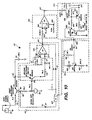
- FIG. 5 shows a preferred version of the first basic embodiment of the invention, where charge status detector 120 is a low-pass filter in combination with a comparator.
- a schematic diagram of a battery charging circuit corresponding to the battery charging system 20 of Figure 1 is shown in Figure 5.
- System 20 includes a preferred embodiment of a state of charge detection and indication circuit 120.
- Power source 40 is a regulated voltage source that provides a uniform or nearly uniform output voltage of 4 Volts DC.
- Current limiting component 70 is a 3 Ohm resistor.
- First electronic switch 50 is a 2N3904 NPN bipolar junction transistor, or any other suitable electronic switching device such as a PNP bipolar junction transistor, or an NMOS or PMOS FET.
- a positive bias must be applied at node 52 (the base of transistor Q1 ) in respect of node 53 (the emitter of transistor Q1 ) to permit current to flow from power source 40 to cell 30.
- Second electronic switch 55 (transistor Q2) forms a portion of cell monitor circuit 110, and is a 2N3906 PNP bipolar junction transistor, or any other suitable electronic switching device, such as an NPN bipolar junction transistor, or an NMOS or PMOS FET. When NPN transistor Q1 is ON, PNP transistor Q2 is OFF.
- System clock 90 is a 100 Hz, 60% duty cycle oscillator providing an output signal of sufficient amplitude to activate Q1 and Q2.
- Reference voltage 80 (or V ref ) is provided at node 82 as a first input to comparator U1 in charge enable control circuit 100.
- V ref is generally set at 1.65 Volts, and may be provided by a zener diode, a voltage regulator, a semiconductor voltage reference generator, or any other suitable device or component.
- comparator U1 is an operational amplifier, but may also be a special purpose integrated circuit, or may be formed from discrete electrical or electronic components.
- capacitor 116 When electronic switch 55 is closed, 1 ⁇ F capacitor 116 either accepts charge from cell 30, or discharges across second electronic switch 55 into cell 30. The direction of current flow, into or out of capacitor 116, depends on the sign of the difference in potential existing between capacitor 116 and cell 30. When second electronic switch 55 closes, capacitor 116 attempts to reach the same potential as cell 30. Thus, at any given time during the charge cycle, capacitor 116 stores a charge approximating the average OCV of cell 30.
- Comparator U1 compares the relative magnitudes of the voltages at nodes 82 and 117. When the voltage at node 82 is less than V ref at node 82, the voltage at node 121(the output of comparator U1) corresponds to the positive saturation voltage of comparator U1. In the preferred embodiment of the present invention, the positive saturation voltage approximates +5 Volts, depending on operating conditions.
- the output of comparator U1 is then in a high state, and charge enable control circuit 100 enables the provision of charge current pulses to cell 30.
- diode 61 (or D1 ) is not forward-biased, and no current flows through it. Thus, the voltage at node 52 is sufficiently high to forward-bias transistor Q1 when the output signal system clock 90 is positive.
- the voltage at node 121 changes from the positive saturation voltage of comparator U1 to its negative saturation voltage.
- the negative saturation voltage approximates zero Volts, depending on operating conditions.
- the output of comparator U1 then changes to a low state, and charge enable control circuit 100 disables the provision of charge current pulses to cell 30.
- diode 61 is forward-biased and therefore conducts current during positive portions of the system clock's output signal. This results in the base of transistor Q1 being held low, whether or not the output signal provided by system clock 90 is high or low. Transistor Q1 therefore remains off until diode 61 stops conducting current.
- charge status detector 120 the output of comparator U1 (the voltage at node 121) is low-pass filtered in charge status detector 120.
- charge status detector 120 most preferably comprises comparator U2 and a single-pole low-pass filter network comprising 100 k ⁇ resistor 122 and 10 ⁇ F capacitor 123.
- Other configurations of the low-pass filter network fall within the scope of the invention, such as multiple pole low-pass or time-averaging filters.
- the low-pass filtered signal at node 125 is a first input to comparator U2.
- a second input to comparator U2 is a voltage signal at node 126 approximating 1.25 Volts (V min ).
- V min may be derived from V ref .
- the output signal of comparator U2 controls charge status indicator 25, which indicates that cell 30 has attained a full state of charge by, for example, driving LED 129 into the ON state from the OFF state, or, conversely (and as shown in Figures 4 and 5) by driving LED 129 into the OFF state from the ON state (as shown in Figures 4 and 5).
- the output of comparator U2 remains high.
- LED 129 (or D2) in charge status indicator 25 then remains lit, and provides a visual indication that cell 30 has not attained a full state of charge.
- the output of comparator U2 changes to a low state.
- LED 129 then turns off, and provides a visual indication that cell 30 has attained a full state of charge.
- FIG. 6 shows a preferred version of the second basic embodiment of the invention, where charge status detector 120 comprises a microprocessor, digital signal processor, or other software programmable device.
- Microprocessor 140 determines a time-averaged value corresponding to the charge enable control signal present at node 121, and compares it to a predetermined reference value. Microprocessor 140 determines the sign and/or magnitude of the difference between the time-averaged value and the predetermined reference value. When the time-averaged value is less than the predetermined reference value, the output signal from the microprocessor appearing at node 127 changes state. This change in state is used to indicate that cell 30 has attained a full state of charge.
- the output signal of microprocessor 140 remains high.
- LED 129 (or D2) in charge status indicator 25 then remains lit, and provides a visual indication that cell 30 has not attained a full state of charge.
- the output signal of microprocessor 140 changes to a low state.
- LED 129 then turns off, and provides a visual indication that cell 30 has attained a full state of charge.
- microprocessor 140 executes logical instructions at a rate of one instruction every two clock cycles, and input/output (I/O) operations and branch instructions every 3 clock pulses.
- Microprocessor 140 samples the analog voltage at node 121 (the charge enable control signal), and converts it into a corresponding digital equivalent by means of an internal AID converter.
- System clock 90 operates at a frequency of 100 Hz with a 60% duty cycle. System clock 90 therefore outputs a sequence of repeating signals having an ON pulse 6 milliseconds in duration followed by an OFF pulse 4 milliseconds in duration. The period of the repeating signal is therefore 10 ms.
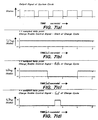
- FIG. 7(a) shows the output signal of system clock 90.
- Microprocessor 140 samples the charge enable control signal at node 121 once every millisecond. This corresponds to a sample rate ten times greater than the fundamental frequency established by system clock 90, thereby preventing any possibility of the charge enable control signal being aliased in microprocessor 140.
- Figure 7(b) shows when microprocessor 140 samples the charge enable control signal during the beginning of the charge cycle. Dots indicate the times at which the charge enable control signal is sampled by the microprocessor. As illustrated in Figure 7(b), in the beginning of the charge cycle the state of charge of cell 30 is low, and the charge enable control signal is almost always high. In the example of Figure 7(b), the time-averaged value corresponding to the average charge enable control signal is +5 Volts, or 50 samples at +5 Volts divided by 50. Microprocessor 140 compares the +5 Volt time-averaged value to a predetermined reference value of 0.5 Volts, determines that the time-averaged value exceeds the predetermined reference value, and causes a high +5 Volt signal to appear at its output. The output signal from microprocessor 140 appearing at node 127 is high, and drives LED 129 ON. LED 129 remains lit to indicate that the state of charge of cell 30 is less than full.
- Figure 7(c) shows when microprocessor 140 samples the charge enable control signal during the middle of the charge cycle. Dots indicate the times at which the charge enable control signal is sampled by the microprocessor. As illustrated in Figure 7(c), in the middle of the charge cycle the state of charge of cell 30 is somewhere between low and full, and the charge enable control signal alternates between high and low. In the example of Figure 7(c), the time-averaged value corresponding to the average charge enable control signal is 2.9 Volts, or 29 samples at +5 Volts and 21 samples at 0 Volts divided by 50.
- Microprocessor 140 compares the +2.9 Volt time-averaged value to a predetermined reference value of 0.5 Volts, determines that the time-averaged value exceeds the predetermined reference value, and causes a high +5 Volt signal to appear at its output.
- the output signal from microprocessor 140 appearing at node 127 is high, and drives LED 129 ON. LED 129 remains lit to indicate that the state of charge of cell 30 is less than full.
- Figure 7(d) shows when microprocessor 140 samples the charge enable control signal during the end of the charge cycle. Dots indicate the times at which the charge enable control signal is sampled by the microprocessor. As illustrated in Figure 7(d), at the end of the charge cycle the state of charge of cell 30 is almost full, and the charge enable control signal almost always low. In the example of Figure 7(d), the time-averaged value corresponding to the average charge enable control signal is 0.4 Volts, or 46 samples at 0 Volts and 4 samples at +5 Volts divided by 50.
- Microprocessor 140 compares the +0.4 Volt time-averaged value to a predetermined reference value of 0.5 Volts, determines that the time-averaged value is less than the predetermined reference value, and causes a low 0 Volt signal to appear at its output.
- the output signal from microprocessor 140 appearing at node 127 is low, and drives LED 129 OFF, thereby indicating that the state of charge of cell 30 is full.
- Table 1 below is an example of a set of high-level functional statements approximating the low-level machine code statements used in microprocessor 140 for sampling the charge enable control signal, computing a time-averaged value thereof, comparing the time-averaged value to a predetermined reference value, and providing an output signal for driving a state of charge indicator.
- Table 1 samples are acquired during the SAMPLE loop.
- the SAMPLE loop requires 10 clock cycles to complete, or 1 millisecond.
- microprocessor 140 samples the charge enable control signal ten times during every period of the output signal of system clock 90. Fifty samples acquired by microprocessor 140 correspond to 5 complete cycles of the output signal of system clock 90.
- the threshold for turning LED 129 off is set at 0.5 Volts, when the charge enable control signal is high only ten percent of the time during which it is sampled.
- the threshold can be set at any desired level, depending on the particular application, and cell chemistry or type involved.
- microprocessors suitable for use in charge status detector 120 include, but are not limited to, the Zilog 28 family of microprocessors, Signetics 87C752 microprocessors, and SGS Thomson ST6 microprocessors.
- Devices other than LEDs may be used as means for indicating the state of charge of cell 30, such as audio alarms or buzzers, incandescent bulbs or electromechanical actuators.
- An electromechanical actuator may move into a "full charge” position from a “less than full charge” position when a full state of charge has been attained in cell 30.
- the polarity of charge status indicator 120 may be reversed so that the indicator is not lit during the charging, but becomes lit when a full state of charge has been attained in cell 30.
- Various other modifications, some of which are described below, may be made to charge status detector 120, without departing from the scope and spirit of the present invention.
- the base drive signal at node 52 may be the input signal (or charge signal) to charge status detector 120 instead of the charge enable control signal at node 121.
- Figure 8 shows such an alternative embodiment of charge status detector 120.
- the charge enable control signal appearing at the output of comparator U1 is not fed to the input of the low-pass filter network comprising resistor 122 and capacitor 123. Instead, the charge enable control signal is routed directly to node 52 through diode 61.
- the input signal to the low-pass filter network of charge status indicator 120 is the signal appearing at node 124, which is the same as the transistor base drive signal appearing at node 52.
- a current transformer may be placed between node 53 and cell 30 to monitor the charge pulses provided to the cell.
- a charge signal corresponding to the charge pulses is the input to charge status detector 120.
- a latching circuit such as a flip-flop, an SCR, or an IC device performing a latching function, may be disposed at node 127 between charge status detector 120 and charge status 25.
- Figure 9 shows a preferred version of latching circuit 150.
- Transistor 155 (or Q3) is a 2N3906 PNP BJT, and transistor 158 (or Q4) is a 2N3904 NPN BJT.
- the voltage appearing at node 160 is initially high at +5 Volts.
- the output of charge status detector goes low because a full state of charge in cell 30 has been detected, the voltage appearing at the base of transistor Q3 changes from +5 Volts to 0 Volts, causing transistor Q3 to turn on.
- transistor Q4 In response to transistor Q3 turning on, the base-emitter junction of transistor Q4 becomes forward biased and transistor Q4 turns on. As soon as transistor Q4 turns on, the voltage appearing at node 166 changes from +5 Volts to 0 Volts. LED 163 then turns off, and visually indicates that cell 30 has attained a full state of charge. The voltage at node 166 stays low until latching circuit 150 is reset by closing and opening reset switch 159, by resetting power to battery charging system 20, or by removing cell 30 from battery charging system 20.
- Hysteretic control may also be implemented in comparator U2. For example, when the average value of the charge enable signal becomes less than V min , the output of comparator U2 having hysteretic control causes LED 129 or 163 to turn off. Thereafter, comparator U2 having hysteretic control does not permit LED 129 or 163 to become relit until the charge enable signal attains a value greater than V min by some predetermined amount or percentage (e.g., the hysteresis window magnitude).
- Overcharging of cell 30 may be prevented by modifying the circuits of Figures 5, 6, 8, or 9 such that the output of charge status detector 120 or latching circuit 150 is used to turn power supply 40 off when a full state of charge in cell 30 is detected.
- Figures 10 and 11 show two such overcharge protection circuits.
- AND gate 167 receives the voltage at node 166 and the charge enable control signal as two inputs.
- latching circuit 150 produces a low voltage at node 166 in response to a full state of charge in cell 30 being detected at charge status detector 120
- AND gate 167 produces a low output signal at the cathode of diode 61, even if the charge enable control signal goes high.
- AND gate 167 produces a low output signal, the voltage at node 52 is pulled down and remains low until AND gate 167 produces a high output, thereby disabling the provision of additional current to cell 30 through transistor Q1. If the output of AND gate 167 is high, diode 61 is reverse biased, and transistor Q1 is modulated by the output signal of system clock 90.
- Figure 11 shows an alternative means of performing the same logical function provided by AND gate 167 in Figure 10.
- diode 168 (or D6) lies between nodes 166 and 169.
- the voltage at node 166 changes from +5 to 0 Volts
- the voltages at node 169 and 52 are pulled down to ground. This disables the provision of additional current to cell 30 through transistor Q1.
- Transistor Q1 does not conduct current from power supply 40 to cell 30 again until its base-emitter junction becomes forward biased (e.g., when the voltage at node 166 goes back up to +5 Volts).
- the program PSPICE was used to model the response of the battery charging system 20 and cell 30 shown in Figure 5.
- Input parameters to the PSPICE program were chosen according to the circuit and corresponding values of discrete components shown in Figure 5.
- Cell 30 was modeled using an equivalent circuit comprising resistors, capacitors, and a voltage source.
- each charge pulse may be on the order of a few milliseconds, while the time required for cell 30 to reach a full state of charge may be several hours.
- the equivalent circuit for cell 30 was adjusted so that the duration of the charge cycle was reduced significantly relative to what it is in actual practice.
- the reduced charge cycle duration permitted a reasonable number of individual charge pulses and instantaneous cell and circuit voltage and current signals to be observed in plots generated by PSPICE. This eliminated the need to observe hundreds of thousands of pulses, voltages, and currents that would otherwise have been generated over an entire charge cycle.
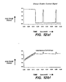
- Figures 12(a) through 12(d) show responses calculated by PSPICE over the initial portion of the charge cycle only for different portions of the circuit shown in Figure 5. Time scales in Figures 12(a) - 12(d) correspond to one another.
- Figure 12(a) shows the voltage at node 121 (the charge enable control signal) calculated by PSPICE.
- the charge enable control signal remains high until about 0.13 seconds, when the output of comparator U1 changes to the low state, and charging of cell 30 through first electronic switch 50 is disabled.
- the output signal of system clock 90 is superimposed on the charge enable control signal whenever the output of comparator U1 is low.
- the charge enable control signal goes high in response to V min being less than the open circuit voltage of cell 30.
- the charge enable signal remains high for a brief period of time, and then goes low.
- Figure 12(b) shows the voltage across cell 30 at node 53 calculated by PSPICE.
- the voltage of cell 30 increases initially until an OCV corresponding to V ref is attained. Thereafter, the corresponding charge enable control signal, as shown in Figure 12(a), is held in the OFF state until the voltage of cell 30 relaxes sufficiently to trigger the output of comparator U1 to change to the high state.
- the state of charge of cell 30 increases during the charge cycle, the time required for the voltage of cell 30 to relax below V ref gradually increases. This, in turn, results in a gradual decrease in the effective duty cycle of the charge enable control signal, as shown in Figure 12(a).
- Figure 12(c) shows the low-pass filtered charge enable control signal at node 125 (v filtered ) calculated by PSPICE. V filtered decreases slowly and relatively smoothly respecting time.
- Figure 12(d) shows the current through LED 129 calculated by PSPICE. In Figure 12(d), LED 129 remains ON during the initial portion of the charge cycle.
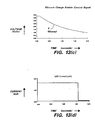
- Figures 13(a) through 13(d) show responses calculated by PSPICE over the entire charge cycle for different portions of the circuit shown in Figure 5. Time scales in Figures 13(a) -13(d) correspond to one another.
- Figure 13(a) shows the voltage at node 121 (the charge enable control signal) calculated by PSPICE.
- Figure 13(a) shows that as time increases the time between charge pulses gradually increases.
- Figure 13(b) shows the voltage across cell 30 at node 53 calculated by PSPICE.
- the voltage of cell 30 rises quickly, and then plateaus.
- the plateau has small pulses superimposed upon it, where the voltage of cell 30 rises quickly, and then decays.
- the timing of the onset of the superimposed pulses corresponds to the charge pulses shown in Figure 13(a).
- the average of the voltage signal shown in Figure 13(b) corresponds roughly to the voltage profile shown in Figure 2, supra.
- Figure 13(c) shows the low-pass filtered charge enable control signal (V filtered ) at node 125 calculated by PSPICE.
- V fi l tered decreases slowly and relatively smoothly respecting time. As the time between charge pulses increases, the average value of V filtered decreases. When V filtered at node 125 drops to 1.25 volts (the value corresponding to V min ), the output of charge status detector 120 changes to the low state, and LED 129 turns off.
- Figure 13(d) shows the current delivered to LED 129, as calculated by PSPICE between nodes 127 and 128 through 200 ⁇ resistor 131.
- Figure 13(d) shows that LED 129 remains ON during the initial portion of the charge cycle, but turns OFF at about 1.6 seconds, when V filtered equals V min .
- the particular embodiment of the invention set forth herein relates to a circuit for detecting or indicating the state of charge of one or a plurality of rechargeable alkaline manganese dioxide cells.
- a circuit for detecting or indicating the state of charge of one or a plurality of rechargeable alkaline manganese dioxide cells Those of ordinary skill in the art will recognize immediately, however, that the present invention is not limited in scope or spirit to applications for rechargeable alkaline manganese dioxide cells only.
- the present invention includes within its scope battery or electrochemical cell state of charge detection and indication circuits for all types of electrochemical cells and batteries.
- the invention may be used in any circuit or battery charging system that utilizes a voltage-controlled, pulse modulated method of charging, secondary battery charging systems for rechargeable lithium ion or rechargeable lithium batteries, or battery "fuel gauging" systems for detecting or indicating the instantaneous state of charge of a battery or cell.
Applications Claiming Priority (2)
| Application Number | Priority Date | Filing Date | Title |
|---|---|---|---|
| US415852 | 1995-04-03 | ||
| US08/415,852 US5661393A (en) | 1995-04-03 | 1995-04-03 | Circuit and method for detecting and indicating the state of charge of a cell or battery |
Publications (2)
| Publication Number | Publication Date |
|---|---|
| EP0736951A2 true EP0736951A2 (fr) | 1996-10-09 |
| EP0736951A3 EP0736951A3 (fr) | 1997-10-29 |
Family
ID=23647474
Family Applications (1)
| Application Number | Title | Priority Date | Filing Date |
|---|---|---|---|
| EP96302399A Withdrawn EP0736951A3 (fr) | 1995-04-03 | 1996-04-03 | Circuit et procédé de détection et d'indication de l'état de charge d'une cellule ou d'une batterie |
Country Status (2)
| Country | Link |
|---|---|
| US (1) | US5661393A (fr) |
| EP (1) | EP0736951A3 (fr) |
Cited By (2)
| Publication number | Priority date | Publication date | Assignee | Title |
|---|---|---|---|---|
| EP1047173A2 (fr) * | 1999-04-21 | 2000-10-25 | Samsung SDI Co., Ltd. | Méthode de génération des données pour l'usage pendant la surveillance et le réglage de l'état de charge et de décharge d'un accumulateur secondaire |
| WO2002071087A1 (fr) * | 2001-03-08 | 2002-09-12 | Daimlerchrysler Ag | Procede et dispositif pour determiner l'effet tampon d'une batterie |
Families Citing this family (14)
| Publication number | Priority date | Publication date | Assignee | Title |
|---|---|---|---|---|
| US6249089B1 (en) | 1998-10-09 | 2001-06-19 | Frederick Bruwer | Intelligent electrical device comprising microchip |
| US6984900B1 (en) * | 1998-10-09 | 2006-01-10 | Azoteq (Pty) Ltd. | Intelligent electrical switch |
| US6154675A (en) * | 1998-10-27 | 2000-11-28 | Medtronic, Inc. | Resetting ERI/POR/PIR/indicators in implantable medical devices |
| US6016448A (en) * | 1998-10-27 | 2000-01-18 | Medtronic, Inc. | Multilevel ERI for implantable medical devices |
| US6091229A (en) * | 1999-03-30 | 2000-07-18 | Motorola, Inc. | Sub-miniature high efficiency battery charger system and method |
| US6669663B1 (en) * | 1999-04-30 | 2003-12-30 | Medtronic, Inc. | Closed loop medicament pump |
| WO2001097379A2 (fr) * | 2000-06-13 | 2001-12-20 | Azoteq (Pty) Ltd | Commutateur intelligent servant a commuter electriquement une charge |
| US7126310B1 (en) | 2001-04-20 | 2006-10-24 | Abiomed, Inc. | Apparatus and method for balanced charging of a multiple-cell battery pack |
| US7019542B2 (en) * | 2004-04-06 | 2006-03-28 | Cadex Electronics Inc. | Method and apparatus for battery testing |
| US20060245131A1 (en) | 2005-04-29 | 2006-11-02 | Ramey Blaine E | Electrical protection circuitry for a docking station base of a hand held meter and method thereof |
| US7679369B2 (en) * | 2006-10-06 | 2010-03-16 | Enerdel, Inc. | System and method to measure series-connected cell voltages using a flying capacitor |
| US8115492B2 (en) * | 2008-01-25 | 2012-02-14 | Eveready Battery Company, Inc. | Fuel gauging system and method thereof |
| US9641011B2 (en) * | 2011-06-10 | 2017-05-02 | Hitachi Automotive Systems, Ltd. | Battery control device adapting the battery current limit by decreasing the stored current limit by comparing it with the measured battery current |
| US11121569B2 (en) | 2018-04-04 | 2021-09-14 | International Business Machines Corporation | Battery state-of-charge indication |
Citations (8)
| Publication number | Priority date | Publication date | Assignee | Title |
|---|---|---|---|---|
| US3621359A (en) * | 1969-03-28 | 1971-11-16 | Leclanche Sa | Method of detecting the end-of-charge condition of an electric storage battery under charge and device for the carrying out of this method |
| US4499415A (en) * | 1982-02-15 | 1985-02-12 | Minicam Research Corporation | Battery rapid charging circuit |
| WO1987005452A1 (fr) * | 1986-03-04 | 1987-09-11 | Erik Denneborg | Appareil regenerateur de cellules primaires |
| EP0311460A2 (fr) * | 1987-10-09 | 1989-04-12 | Norvik Technologies Inc. | Chargeur de batterie |
| JPH05103430A (ja) * | 1991-10-07 | 1993-04-23 | Murata Mfg Co Ltd | バツテリ充電回路 |
| DE4136122A1 (de) * | 1991-11-02 | 1993-05-06 | Dipl.-Ing. W. Sorg Gmbh, 7987 Weingarten, De | Verfahren zum schnelladen von gasdichten akkumulatoren, insbesondere nicd- oder nih-akkumulatoren |
| US5376875A (en) * | 1993-12-03 | 1994-12-27 | Motorola, Inc. | Battery charger status monitor circuit and method therefor |
| US5396163A (en) * | 1991-03-13 | 1995-03-07 | Inco Limited | Battery charger |
Family Cites Families (8)
| Publication number | Priority date | Publication date | Assignee | Title |
|---|---|---|---|---|
| CA981746A (en) * | 1973-09-24 | 1976-01-13 | Alfred M. Hase | Battery charging circuit |
| US4016473A (en) * | 1975-11-06 | 1977-04-05 | Utah Research & Development Co., Inc. | DC powered capacitive pulse charge and pulse discharge battery charger |
| DE2748644A1 (de) * | 1977-10-29 | 1979-05-03 | Varta Batterie | Verfahren zur ladungserhaltung und zur dauerladung von akkumulatoren |
| US4554500A (en) * | 1983-03-31 | 1985-11-19 | Anton/Bauer, Inc. | Battery charging apparatus and method |
| US4679000A (en) * | 1985-06-20 | 1987-07-07 | Robert Clark | Bidirectional current time integration device |
| GB8625035D0 (en) * | 1986-10-18 | 1986-11-19 | Husky Computers Ltd | Battery charge state monitor |
| CA1311268C (fr) * | 1988-04-11 | 1992-12-08 | Karl Kordesch | Appareil de recharge a tension constante d'accumulateurs |
| US5248928A (en) * | 1990-09-18 | 1993-09-28 | Black & Decker Inc. | Timed battery charger |
-
1995
- 1995-04-03 US US08/415,852 patent/US5661393A/en not_active Expired - Fee Related
-
1996
- 1996-04-03 EP EP96302399A patent/EP0736951A3/fr not_active Withdrawn
Patent Citations (8)
| Publication number | Priority date | Publication date | Assignee | Title |
|---|---|---|---|---|
| US3621359A (en) * | 1969-03-28 | 1971-11-16 | Leclanche Sa | Method of detecting the end-of-charge condition of an electric storage battery under charge and device for the carrying out of this method |
| US4499415A (en) * | 1982-02-15 | 1985-02-12 | Minicam Research Corporation | Battery rapid charging circuit |
| WO1987005452A1 (fr) * | 1986-03-04 | 1987-09-11 | Erik Denneborg | Appareil regenerateur de cellules primaires |
| EP0311460A2 (fr) * | 1987-10-09 | 1989-04-12 | Norvik Technologies Inc. | Chargeur de batterie |
| US5396163A (en) * | 1991-03-13 | 1995-03-07 | Inco Limited | Battery charger |
| JPH05103430A (ja) * | 1991-10-07 | 1993-04-23 | Murata Mfg Co Ltd | バツテリ充電回路 |
| DE4136122A1 (de) * | 1991-11-02 | 1993-05-06 | Dipl.-Ing. W. Sorg Gmbh, 7987 Weingarten, De | Verfahren zum schnelladen von gasdichten akkumulatoren, insbesondere nicd- oder nih-akkumulatoren |
| US5376875A (en) * | 1993-12-03 | 1994-12-27 | Motorola, Inc. | Battery charger status monitor circuit and method therefor |
Non-Patent Citations (1)
| Title |
|---|
| PATENT ABSTRACTS OF JAPAN vol. 17, no. 460 (E-1419), 23 August 1993 & JP 05 103430 A (MURATA MFG), 23 April 1993, * |
Cited By (5)
| Publication number | Priority date | Publication date | Assignee | Title |
|---|---|---|---|---|
| EP1047173A2 (fr) * | 1999-04-21 | 2000-10-25 | Samsung SDI Co., Ltd. | Méthode de génération des données pour l'usage pendant la surveillance et le réglage de l'état de charge et de décharge d'un accumulateur secondaire |
| EP1047173A3 (fr) * | 1999-04-21 | 2001-04-11 | Samsung SDI Co., Ltd. | Méthode de génération des données pour l'usage pendant la surveillance et le réglage de l'état de charge et de décharge d'un accumulateur secondaire |
| US6456948B1 (en) | 1999-04-21 | 2002-09-24 | Samsung Sdi Co., Ltd. | Method of generating data for use in monitoring and controlling charge and discharge status of secondary battery |
| WO2002071087A1 (fr) * | 2001-03-08 | 2002-09-12 | Daimlerchrysler Ag | Procede et dispositif pour determiner l'effet tampon d'une batterie |
| US7199588B2 (en) | 2001-03-08 | 2007-04-03 | Daimlerchrysler Ag | Method and system for determining the buffer action of a battery |
Also Published As
| Publication number | Publication date |
|---|---|
| EP0736951A3 (fr) | 1997-10-29 |
| US5661393A (en) | 1997-08-26 |
Similar Documents
| Publication | Publication Date | Title |
|---|---|---|
| US5661393A (en) | Circuit and method for detecting and indicating the state of charge of a cell or battery | |
| US4413221A (en) | Method and circuit for determining battery capacity | |
| US5523671A (en) | Charging system for battery powered devices | |
| US5449997A (en) | Battery charging system having logarithmic analog-to-digital converter with automatic scaling of analog signal | |
| KR100221047B1 (ko) | 배터리를 충전하고 테스트하는 방법 및 장치 | |
| US5864220A (en) | Method and apparatus for controlling the charging of a rechargeable battery to ensure that full charge is achieved without damaging the battery | |
| US5160880A (en) | Method and apparatus for charging and testing batteries | |
| CA1330828C (fr) | Chargeur de batterie | |
| US4745349A (en) | Apparatus and method for charging and testing batteries | |
| US5576608A (en) | Method for charging secondary battery and charger used therefor | |
| EP1205017B1 (fr) | Procede et dispositif de chargement rapide de batterie | |
| US5218286A (en) | Multichannel battery charger | |
| EP0669693A1 (fr) | Système pour recharger une batterie ayant des moyens pour détecter l'état de charge pour éviter une surcharge | |
| EP0368353A2 (fr) | Appareil de charge de batterie | |
| US20010000212A1 (en) | Battery system providing indicia of a charging parameter | |
| EP0425044A1 (fr) | Dispositif pour charger une batterie | |
| US5321347A (en) | Battery charger device and method | |
| JP2001516122A (ja) | 細動除去装置中のバッテリパックの状態を監視する方法及びシステム | |
| US6020720A (en) | Fast charging method and apparatus for secondary cells | |
| EP0286282A2 (fr) | Méthode de détection d'une tension d'entrée alternative | |
| JP3539432B2 (ja) | 2次電池の残存容量の判別装置及びこれを用いた充電装置 | |
| JP2003139827A (ja) | 二次電池装置 | |
| US6218808B1 (en) | Micro-peak detection quick charger | |
| KR950009337B1 (ko) | 배터리 충전회로 | |
| JP2890702B2 (ja) | 蓄電池のメモリ効果判別方法並びにメモリ効果警告装置 |
Legal Events
| Date | Code | Title | Description |
|---|---|---|---|
| PUAI | Public reference made under article 153(3) epc to a published international application that has entered the european phase |
Free format text: ORIGINAL CODE: 0009012 |
|
| AK | Designated contracting states |
Kind code of ref document: A2 Designated state(s): DE FR GB |
|
| PUAL | Search report despatched |
Free format text: ORIGINAL CODE: 0009013 |
|
| AK | Designated contracting states |
Kind code of ref document: A3 Designated state(s): DE FR GB |
|
| 17P | Request for examination filed |
Effective date: 19971126 |
|
| 17Q | First examination report despatched |
Effective date: 19980403 |
|
| STAA | Information on the status of an ep patent application or granted ep patent |
Free format text: STATUS: THE APPLICATION IS DEEMED TO BE WITHDRAWN |
|
| 18D | Application deemed to be withdrawn |
Effective date: 19980814 |