EP0732422B1 - Ferroelectric thin-film coated substrate, method for its manufacture and nonvolatile memory comprising such a substrate - Google Patents
Ferroelectric thin-film coated substrate, method for its manufacture and nonvolatile memory comprising such a substrate Download PDFInfo
- Publication number
- EP0732422B1 EP0732422B1 EP96301577A EP96301577A EP0732422B1 EP 0732422 B1 EP0732422 B1 EP 0732422B1 EP 96301577 A EP96301577 A EP 96301577A EP 96301577 A EP96301577 A EP 96301577A EP 0732422 B1 EP0732422 B1 EP 0732422B1
- Authority
- EP
- European Patent Office
- Prior art keywords
- film
- thin
- ferroelectric
- ferroelectric thin
- growth layer
- Prior art date
- Legal status (The legal status is an assumption and is not a legal conclusion. Google has not performed a legal analysis and makes no representation as to the accuracy of the status listed.)
- Expired - Lifetime
Links
Images


Classifications
-
- C—CHEMISTRY; METALLURGY
- C23—COATING METALLIC MATERIAL; COATING MATERIAL WITH METALLIC MATERIAL; CHEMICAL SURFACE TREATMENT; DIFFUSION TREATMENT OF METALLIC MATERIAL; COATING BY VACUUM EVAPORATION, BY SPUTTERING, BY ION IMPLANTATION OR BY CHEMICAL VAPOUR DEPOSITION, IN GENERAL; INHIBITING CORROSION OF METALLIC MATERIAL OR INCRUSTATION IN GENERAL
- C23C—COATING METALLIC MATERIAL; COATING MATERIAL WITH METALLIC MATERIAL; SURFACE TREATMENT OF METALLIC MATERIAL BY DIFFUSION INTO THE SURFACE, BY CHEMICAL CONVERSION OR SUBSTITUTION; COATING BY VACUUM EVAPORATION, BY SPUTTERING, BY ION IMPLANTATION OR BY CHEMICAL VAPOUR DEPOSITION, IN GENERAL
- C23C16/00—Chemical coating by decomposition of gaseous compounds, without leaving reaction products of surface material in the coating, i.e. chemical vapour deposition [CVD] processes
- C23C16/22—Chemical coating by decomposition of gaseous compounds, without leaving reaction products of surface material in the coating, i.e. chemical vapour deposition [CVD] processes characterised by the deposition of inorganic material, other than metallic material
- C23C16/30—Deposition of compounds, mixtures or solid solutions, e.g. borides, carbides, nitrides
- C23C16/40—Oxides
-
- C—CHEMISTRY; METALLURGY
- C23—COATING METALLIC MATERIAL; COATING MATERIAL WITH METALLIC MATERIAL; CHEMICAL SURFACE TREATMENT; DIFFUSION TREATMENT OF METALLIC MATERIAL; COATING BY VACUUM EVAPORATION, BY SPUTTERING, BY ION IMPLANTATION OR BY CHEMICAL VAPOUR DEPOSITION, IN GENERAL; INHIBITING CORROSION OF METALLIC MATERIAL OR INCRUSTATION IN GENERAL
- C23C—COATING METALLIC MATERIAL; COATING MATERIAL WITH METALLIC MATERIAL; SURFACE TREATMENT OF METALLIC MATERIAL BY DIFFUSION INTO THE SURFACE, BY CHEMICAL CONVERSION OR SUBSTITUTION; COATING BY VACUUM EVAPORATION, BY SPUTTERING, BY ION IMPLANTATION OR BY CHEMICAL VAPOUR DEPOSITION, IN GENERAL
- C23C16/00—Chemical coating by decomposition of gaseous compounds, without leaving reaction products of surface material in the coating, i.e. chemical vapour deposition [CVD] processes
- C23C16/02—Pretreatment of the material to be coated
- C23C16/0272—Deposition of sub-layers, e.g. to promote the adhesion of the main coating
Definitions
- the present invention refers to a ferroelectric thin-film coated substrate used in a ferroelectric memory element, a pyroelectric sensor element, a piezoelectric element and the like, and a manufacturing method thereof and the nonvolatile memory comprising a ferroelectric thin-film coated substrate.
- ferroelectrics are applied to a wide development of devices such as capacitor, oscillator, optical modulator or infrared sensor. So far, for use in these applications, single crystal, such as triglycine sulfate (TGS), LiNbO 3 and LiTaO 3 or sintered ceramics such as BaTiO 3 , PbTiO 3 , Pb(Zr 1-x Ti x )O 3 (PZT) and PLZT, ferroelectric material, has been machined to the order of 50 ⁇ m in thickness by cutting and grinding.
- TGS triglycine sulfate
- LiNbO 3 and LiTaO 3 LiTaO 3
- sintered ceramics such as BaTiO 3 , PbTiO 3 , Pb(Zr 1-x Ti x )O 3 (PZT) and PLZT
- ferroelectric nonvolatile memories FLC
- Ferroelectric nonvolatile memories need no backup power supply by making use of a ferroelectric characteristic (hysteresis effect) of ferroelectrics.
- oxide ferroelectrics such as PbTiO 3 , PZT and PLZT into a thin-film by the thin-film forming method such as sputtering, evaporation, sol-gel process and MOCVD.
- PZT Pb(Zr 1-x Ti x ) O 3
- Y1 is a Bi-based layered oxide material, expressed in chemical formula SrBi 2 Ta 2 O 9 , and produced by MOD process.
- the MOD process is a thin-film forming method comprising the following steps. As with the sol-gel process, organic metal materials are mixed to form a predetermined thin-film composition and a material solution for coating with the concentration and the viscosity adjusted is prepared. This solution is spin coated to the ground plate, dried and provisionally sintered. These steps are repeated till the thin-film has reached a predetermined thickness and finally the crystallization by a true sintering is accomplished. Accordingly, control of the thin-film thickness is restricted by the thickness of a one-time coated thin-film (cf. 1994 Autumn Applied Physics Meeting Preprints, 20p-M-19).
- the sintering temperature is extremely high as 750°C to 800°C and a further long sintering time of an hour or longer is necessary. That is because, when the steps of thin-film formation and heat treatment are performed at 650°C or higher temperatures for a long period of time in such production process, a mutual diffusion reaction between the underlying platinum electrode and ferroelectrics and further a reaction between silicon or silicon oxide below the underlying electrode and ferroelectrics take place, and a change in thin-film composition due to the volatilization of component element from the ferroelectrics thin-film occurs, so that application to the actual production process of devices becomes difficult.
- oxide ferroelectrics not containing Pb adversely affecting the leak current and resistance to polarization inversion include a group of bismuth based oxide ferroelectrics having layered crystal structures expressed in the following general chemical formula.
- A is selected from Na 1+ , K 1+ , Pb 2+ , Ca 2+ , Sr 2+ , Ba 2+ , Bi 3+ and the like
- B is selected from Fe 3+ , Ti 4+ , Nb 5+ , Ta 5+ , W 6+ and Mo 6+
- m is an integer not less than 1.
- Their crystal structure have a fundamental structure in which a layered perovskite layer in an array of perovskite lattices composed of (m-1) ABO 3 is sandwiched by two layers of (Bi 2 O 2 ) 2+ from above and from below.
- Sr, Ba or Bi as A with Ti, Ta or Nb as B exhibit ferroelectricity.
- the above Y1 is one type of these bismuth based oxide ferroelectrics.
- Bi 4 Ti 3 O 12 bismuth titanate
- a c-axis oriented Bi 4 Ti 3 O 12 thin-film is prepared at substrate temperatures of 600°C or higher on a Pt/SiO 2 /Si substrate or on a Pt substrate, but these substrates cannot be directly applied to an actual device structure. That is, as with the Pt/Ti/SiO 2 /Si substrate, an adhesive layer, such as Ti layer, for ensuring the adhesive strength between the Pt electrode layer and its underlying SiO 2 layer is necessary.
- the thin-film surface morphology comprises coarse crystal grains
- application to a highly integrated device requiring a fine machining is impossible and moreover pin holes are still more apt to be caused for the thinner thin-film and consequently occurrence of leak current is induced.
- the pyrochlore phase exhibits no ferroelectricity, mixing of the pyrochlore phase leads to deterioration of ferroelectricity on the whole thin-film.
- the above prior art has a problem that, in applying a ferroelectric thin-film to highly integrated devices, those satisfactorily meeting the denseness and the evenness of the surface of a thin-film required for fine machining or low leak current, a large residual spontaneous polarization, and various requirements for the low-temperature thin-film forming process are not yet obtained.
- a ferroelectric substrate having a dense and even surface and a large residual spontaneous polarization which can be prepared in the low-temperature thin-film forming process, and the manufacture method thereof, and a nonvolatile memory composed thereof.
- the present invention provides a ferroelectric thin-film coated substrate as set out in claim 1.
- the layered crystal structure expressed in a chemical formula Bi 2 A m-1 B m O 3m+3 where A is selected from Na 1+ , K 1+ , Pb 2+ , Ca 2+ , Sr 2+ , Ba 2+ , Bi 3+ and the like, B is selected from Fe 3+ , Ti 4+ , Nb 5+ , Ta 5+ , W 6+ and Mo 6+ , and m is an integer not less than 1, is a crystal structure formed by the alternate stacking of (Bi 2 O 2 ) 2+ layers and (A m-1 B m O 3m+3 ) 2- layers.
- selection of A and B here is not limited to a single way.
- Typical of ferroelectric materials having such a crystal structure is Bi 4 Ti 3 O 12 .
- others are SrBi 2 Nb 2 O 9 , SrBi 2 Ta 2 O 9 , Babi 2 Nb 2 O 9 , BaBi 2 Ta 2 O 9 , Pb 2 Bi 2 Nb 2 O 9 , PbBi 2 Ta 2 O 9 , SrBi 4 Ti 4 O 15 , BaBi 4 Ti 4 O 15 , PbBi 4 Ti 4 O 15 , Na 0.5 B i4.5 Ti 4 O 15 , K 0.5 Bi 4.5 Ti 4 O 15 , Sr 2 Bi 4 Ti 5 O 18 , Ba 2 Bi 4 Ti 5 O 18 and Pb 2 Bi 4 Ti 5 O 18 .
- ferroelectric materials expressed in the same chemical formula, having a layered crystal structure and exhibiting no ferroelectric characteristic include Bi 3 TiNbO 9 , Bi 3 TiTaO 9 , CaBi 2 Nb 2 O 9 , CaBi 2 Ta 2 O 9 and CaBi 4 Ti 4 O 15 .
- Ferroelectric thin-film coated substrates made by forming ferroelectric thin-films composed of these bismuth-based oxide ferroelectric materials on a substrate, the interposition of both a buffer layer and a growth layer for allowing the ferroelectric thin-film to grow between the substrate and the ferroelectric thin-film enables a marked upgrade in crystallinity, ferroelectricity, electrical properties, thin-film properties and the like.
- the present invention can be thought to be effective for those dielectric materials expressed in the above-mentioned chemical formula Bi 2 A m-1 B m O 3m+3 having a layered crystal structure similar to that of a Bi 4 Ti 3 O 12 as the ferroelectric thin-film.
- the growth layer since those indicating a crystal structure resembling that of a ferroelectric thin-film is thought to be preferable, those composed of oxide materials containing the component elements of a ferroelectric thin-film or bismuth-based oxide materials having a layered structure similar to that of a ferroelectric thin-film can be regarded as preferable.
- the buffer layer those composed of the component elements of the ferroelectric thin-film and the growth layer can be regarded as preferable.
- the invention also provides a method for manufacturing a ferroelectric thin film coated substrate as set out in claim 4.
- the invention further provides a method for manufacturing a ferroelectric thin-film coated substrate as set out in claim 8.
- a random orientation thin-film of Bi 4 Ti 3 O 12 ferroelectric thin-film could be formed by forming a growth layer (Bi 4 Ti 3 O 12 thin-film) at thin-film forming temperatures of 400°C to 650°C and a Bi 4 Ti 3 O 12 ferroelectric thin-film at lower temperatures of 300°C to 400°C than the growth layer forming temperature. Furthermore, by controlling the thin-film forming temperature of the growth layer (Bi 4 Ti 3 O 12 thin-film) within the range of 400°C to 650°C, the crystallinity (orientation) of a ferroelectric thin-film was found to be controllable.
- a Bi 4 Ti 3 O 12 ferroelectric thin-film can be formed at by far lower temperatures of 300°C to 400°C than the conventional thin-film forming temperature, a very dense and smooth thin-film can be implemented.
- the above thin-film forming process can be performed at the temperature of 650°C or less, it is very effectively applied to a highly integrated device.
- the randomly oriented component can be intensified and the residual spontaneous polarization of a ferroelectric thin-film can be very greatly increased as compared with a conventional one by effectively utilizing the a-axis oriented component of Bi 4 Ti 3 O 12 .
- the heat treatment step after such a thin-film forming step as mentioned above, the crystallinity of a ferroelectric thin-film can be further enhanced, the residual spontaneous polarization can be increased and the leak current characteristic can be noticeably improved.
- the heat treatment temperature is effective in the range of 500°C to 700°C, and since the effect is obtained by a short-time treatment even around 700°C, no adverse effect is exerted even on a highly integrated device in application.
- capacitor-structured nonvolatile memories according to the present invention can exhibit a sufficient characteristic.
- MFMIS-FET-structured nonvolatile memories according to the present invention can exhibit a sufficient characteristic.
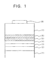
- FIG. 1 shows the structure of a ferroelectrics thin-film substrate according to a first embodiment of the present invention.
- this ferroelectric thin-film coated substrate comprises a silicon oxide (SiO 2 ) layer 2, an adhesive layer 3, a lower electrode layer 4, a buffer layer 5, c growth layer for allowing a ferroelectrics thin-film to grow 6, a ferroelectric thin-film 7 and an upper electrode layer 8 successively formed on a silicon (Si) substrate 1.
- a silicon single crystal wafer was employed as the silicon substrate 1, while a silicon oxide thin-film obtained by thermally oxidizing the surface of the silicon single crystal wafer was employed as the SiO 2 layer 2.
- a tantalum (Ta) thin-film, a platinum (Pt) thin-film, a titanium oxide thin-film, a Bi 4 Ti 3 O 12 thin-film, a Bi 4 Ti 3 O 12 thin-film and a platinum (Pt) thin-film are employed as the adhesive layer 3, the lower electrode layer 4, a buffer layer 5, a growth layer 6, a ferroelectric thin-film 7 and an upper electrode layer 8, respectively.
- a Pt/Ta/SiO 2 /Si substrate By thermal oxidation of the surface of (100) plane in a silicon single crystal wafer as the silicon substrate 1, a SiO 2 layer 2, 200 nm in thin-film thickness, is formed. Then, a Ta thin-film as the adhesive layer 3, 30 nm in thin-film thickness, and a Pt thin-film as the lower electrode layer 4, 200 nm in thin-film thickness, are formed respectively by the sputter method.
- these materials and the thin-film thickness are not limited to this arrangement, but a polycrystalline silicon substrate, a GaAs substrate or the like may be also employed.
- the adhesive layer is provided for preventing the peeling of a thin-film from occurring during the thin-film forming due to a difference in thermal expansion coefficient between the substrate and the lower electrode layer, the thin-film thickness is only necessary to be as thick as capable of preventing the peeling of a thin-film.
- Other materials such as titanium (Ti) than Ta may be employed, but Ta is preferable because Ti and Pt form an alloy.
- the SiO 2 layer employed for the insulating layer may not be prepared by heat treatment, an SiO 2 thin-film, a silicon nitride thin-film or the like are formed by the sputtering process, the vapor deposition process and the like. Any material and any thin-film thickness are allowable so long as a sufficient insulation is ensured.
- the thin-film thickness is only required to be as large as equal to the function of an electrode and the material is not limited to Pt but may be metal materials employed for ordinary electrode materials and can be appropriately selected in relation to other thin-film.
- a thin-film formation method is also not limited to the silicon oxidation process or the sputtering process heretofore and ordinary thin-film forming techniques such as vapor deposition may be employed.
- the structure of a substrate is also not limited to the above-mentioned.
- titanium isopropoxide Ti(i-OC 3 H 7 ) 4
- Ti(i-OC 3 H 7 ) 4 titanium isopropoxide
- the flow rate at the Ar gas supply was set at 100 sccm.
- Pt/Ta/SiO 2 /Si substrate prepared as described above heated and kept at a definite temperature in the thin-film forming chamber a 5 nm thick titanium oxide thin-film was formed on this substrate. At that time, the time taken for the forming step of a titanium oxide was of the order of 30 sec.
- Table 1 shows the supply conditions of raw materials for the thin-film forming by the MOCVD process at this time.
- the flow rate of Ar gas at the supply was set at 200 sccm for Bi raw material and 100 sccm for Ti raw material, while the flow rate of O 2 gas at the supply was set at 1000 sccm.
- the degree of vacuum in the thin-film forming chamber was set at 5 Torr, because the gaseous phase reaction is apt to occur if it is above 1333 Pa (10 Torr).
- the thin-film forming temperature i.e., the substrate temperature at 450°C and 500°C
- two kinds of samples 50 nm in the total thickness of a titanium oxide buffer layer and a Bi 4 Ti 3 O 12 thin-film (growth layer)
- the thin-film thickness of Bi 4 Ti 3 O 12 thin-film (growth layer) was set at 45 nm, and was made rather larger at any rate for purposes of observing the surface morphology and the crystallinity.
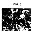
- a control was also prepared in which no titanium oxide buffer layer was formed and a Bi 4 Ti 3 O 12 thin-film was formed directly on the Pt/Ta/SiO 2 /Si substrate in a thickness of 150 nm. Except that no titanium oxide buffer layer was formed and the thin-film forming temperature was set at 500°C, the thin-film forming conditions for this control are quite the same as with the samples mentioned above.
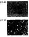
- FIGs. 2A, 2B and 3 show the SEM observed results
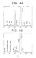
- Figs 4A, 4B and 5 shows the observed results on X-ray diffractometer.
- FIGs. 2A and 4A relate to samples of 450°C
- FIGs. 2B and 4B relate to samples of 500°C, respectively.
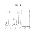
- FIGs. 3 and 5 show the respective observed results of controls without titanium oxide buffer layer.
- the thin-film forming up to the Bi 4 Ti 3 O 12 thin-film of growth layer is carried out in quite the same manner as that described above except for setting the thickness of a Bi 4 Ti 3 O 12 thin-film of growth layer to 5 nm. Also in this case, two types of samples were prepared setting the thin-film forming temperature (the substrate temperature) of a Bi 4 Ti 3 O 12 thin-film (growth layer) at 450°C and 500°C. The time taken for the thin-film forming step of a Bi 4 Ti 3 O 12 thin-film growth layer was around 30 sec for any sample.
- the thin-film forming conditions for a Bi 4 Ti 3 O 12 of ferroelectric thin-film are quite the same as those of a Bi 4 Ti 3 O 12 thin-film of growth layer described using Table 1.
- the time taken for the thin-film forming step of a Bi 4 Ti 3 O 12 thin-film of ferroelectric thin-film was around 30 min for any sample, and therefore the time taken for the thin-film forming step of a buffer layer, a growth layer and a ferroelectric thin-film is nearly equal to 30 min in total for any sample.
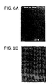
- FIGs. 6A and 6B show the observed results under SEM, while FIGs. 7A and 7B show the observed results on X-ray diffractometer.
- FIGs. 6A and 7A relate to samples of 450°C and FIGs. 6B and 7B relate to samples of 500°C.
- this arrangement showed only the results for the thin-film forming temperature of the growth layer of 450°C and for that of 500°C, but it could be confirmed that the thin-film forming temperature ranging from 400°C to 650°C permits a sufficiently smooth and dense crystallinity of growth layer (Bi 4 Ti 3 O 12 thin-film) to be obtained. Furthermore, at thin-film forming temperature of not lower than 650°C, though the crystallinity is high, the growth of crystalline grains was so much that no smooth-surface growth layer (Bi 4 Ti 3 O 12 thin-film) could be obtained.
- a Bi 4 Ti 3 O 12 of ferroelectric thin-film according to an embodiment of the present invention exhibits a very dense, smooth and good thin-film surface morphology and forms a random orientation thin-film containing components other than that of the c-axis orientation. Furthermore, it was found that those of 450°C in the thin-film forming temperature (substrate temperature) of the Bi 4 Ti 3 O 12 thin-film exhibit a denser and smoother surface morphology than those of 500°C and are superior in random orientation regarding crystallinity.
- Such a capacitor structure as shown in FIG. 1 was constructed by forming an upper electrode layer on the ferroelectric thin-film (Bi 4 Ti 3 O 12 thin-film) for two types of samples prepared in this manner and the electric characteristic of this thin-film was estimated, where a 100 ⁇ m ⁇ Pt electrode thin-film was formed as this electrode by vacuum deposition process.
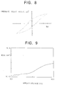
- a sample with the growth layer (Bi 4 Ti 3 O 12 thin-film) formed at 450°C exhibits such a ferroelectric hysteresis curve as shown in FIG. 8.
- FIG. 10 shows the ferroelectric hysteresis curve of a still another sample of this arrangement, i.e., a sample with the growth layer (Bi 4 Ti 3 O 12 thin-film) formed at 500°C.
- Pr is smaller than Pr of FIG. 8
- Ec is also smaller than Ec of FIG. 8.
- This is attributable to a strong c-axis oriented component though the crystallinity of this sample is a random orientation.
- Such a small value of Ec suggests that the sample is applicable to a device operable at low voltage.
- the thin-film forming temperature of a Bi 4 Ti 3 O 12 of growth layer was set at 450°C, a sample having a 40 nm thick Bi 4 Ti 3 O 12 of ferroelectric thin-film and having a 50 nm thick composite of titanium oxide buffer layer and growth layer was prepared. Except that the thickness of a Bi 4 Ti 3 O 12 of ferroelectric thin-film was set at 40 nm, the preparing method was quite the same as with the first embodiment. At that time, the time taken for the step of forming a Bi 4 Ti 3 O 12 ferroelectric thin-film was around 15 min and therefore the time taken for the steps of forming a buffer layer, a growth layer and ferroelectric layer is approximately 15 min in total.
- the ferroelectric hysteresis curve of a sample according to this embodiment obtained from a measurement similar to that of the first embodiment is shown in FIG. 11.
- the repetitive fatigue for polarization inversion was measured on a sample according to this embodiment
- the test conditions are that, when repeatedly applying a pair of bipolar pulses at an applied voltage of 3V and in a pulse width of 100 ns, the changing rate of switching charge quantity (difference between the inversion charge quantity and the non-inversion charge quantity of polarization) is measured.
- the results are shown in FIG. 12.
- a decrease in switching charge quantity is about 13% after 1 ⁇ 10 12 times of repetitions and accordingly the fatigue resistance of this arrangement is clearly by far superior since that of a conventional PZT material is at most on the order of 10 8 .
- FIG. 13 shows the observed results of thin-film surface morphology under SEM in this arrangement. Since the thin-film is thin, this sample comprises fine crystalline grains on the order of nm and a good characteristic of very dense and smooth thin-film was found to be obtained.
- a third embodiment with heat treatment applied to a sample prepared according to the second embodiment will be described.
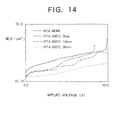
- the RTA Rapid Thermal Annealing
- high-speed heat treatment by infrared irradiation was applied at a heat treatment temperature of 650°C in oxygen gas flow and the ferroelectric characteristic was examined for different periods of treatment time of 2 min, 10 min and 30 min.
- leak current Il varies depending on applied voltage as shown in FIG.14.
- RTA treatment time With longer RTA treatment time, Il was markedly improved. This is attributable to an improvement in the crystallinity of a Bi 4 Ti 3 O 12 of ferroelectric thin-film due to heat treatment in this arrangement.
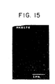
- a sample having a 190 nm thick Bi 4 Ti 3 O 12 ferroelectric thin-film and having a 200 nm composite of titanium oxide buffer layer and growth layer (Bi 4 Ti 3 O 12 ) was prepared. Except that the thin-film forming temperature of a growth layer (Bi 4 Ti 3 O 12 thin-film) was set at 450°C, the preparing method was quite the same as that of the first and second embodiments. At that time, the time taken for the step of forming a Bi 4 Ti 3 O 12 ferroelectric thin-film was of the order of 60 min and therefore the time taken for the steps of forming a buffer layer, a growth layer and ferroelectrics layer is approximately of the order of an hour in total.
- FIG. 15 shows the result of SEM observation of thin-film surface morphology in this embodiment.
- a very dense, smooth and good thin-film surface morphology on the order of 10 nm is exhibited.
- the thin-film thickness was nearly double that of the first embodiment, the surface morphology of the Bi 4 Ti 3 O 12 ferroelectric thin-film is found to be strongly affected by the growth layer (Bi 4 Ti 3 O 12 thin-film).
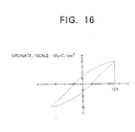
- FIG. 16 shows the ferroelectric hysteresis curve of a sample according to this embodiment, measured as with the above embodiments.
- the present invention could be confirmed to be effective for as thick a ferroelectric thin-film as 200 nm.
- the thickness was set at 5 nm for any of titanium oxide layer and growth layer (Bi 4 Ti 3 O 12 thin-film) but the present invention was significantly obtained even if the thickness of either layer is within the range of 3 nm to 10 nm.
- this embodiment employed a Pt lower electrode layer/Ta adhesive layer/SiO 2 insulating layer/Si substrate as the substrate, but, in spite of a former report that the pyrochlore phase of Bi 4 Ti 3 O 12 was apt to occur when a Bi 2 Ti 2 O 7 thin-film is formed on a similar substrate by low-temperature forming through aids of the MOCVD process, it was proved that no pyrochlore phase of Bi 2 Ti 2 O 7 occurs in this embodiment and the present invention is not limited to such a substrate structure.
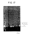
- FIGs. 17 and 18 show the surface morphology and sectional shape of this Bi 4 Ti 3 O 12 thin-film by perspective SEM photography and the X-ray diffraction pattern of this Bi 4 Ti 3 O 12 thin-film.
- a thin-film according to the fifth embodiment is a good crystallinity Bi 4 Ti 3 O 12 thin-film, so-called random orientation thin-film comprising the c-axis (00n) and (117) oriented components and a dense and smooth thin-film.
- the peak intensity ratio of this embodiment was proved to be situated just between that of FIG. 7A and that of FIG. 7B. From this it is considered that the orientation state of a Bi 4 Ti 3 O 12 according to this embodiment is an intermediate state between that shown in FIG. 7A and that shown in FIG. 7B.
- FIG. 21 the measured result of fatigue resistance in the relevant Bi 4 Ti 3 O 12 thin-film is shown in FIG. 21.
- a change in residual polarization was such a degree that about 3.2% decrease of Pr was noticed after 1 ⁇ 10 12 times of repetitions and accordingly the fatigue characteristic of ferroelectric thin-films according to embodiments of the present invention is proved to be extremely excellent as compared with a conventional PZT material (the fatigue resistance limit is below 10 8 times).
- a sixth embodiment will be described hereinafter.
- a Bi 4 Ti 3 O 12 ferroelectric thin-film was formed so as to obtain a total thickness of 50 nm.
- FIG. 22 shows the surface morphology and sectional shape of this Bi 4 Ti 3 O 12 thin-film by perspective SEM photography.
- a dense, smooth-surface, good crystallinity and random orientation Bi 4 Ti 3 O 12 thin-film was obtained.
- a sufficient ferroelectric characteristic can be effectively drawn out by using a very thin-film as 50 nm thick thin-film, which is the most important merit also in application to a large capacity FRAM or the like.
- a seventh embodiment will be described hereinafter.
- a 5 nm thick Bi 4 Ti 3 O 12 growth layer was formed subsequently by simultaneously supplying a Bi raw material, a Ti raw material and O 2 gas at a substrate temperature of 450°C.
- a Bi 4 Ti 3 O 12 thin-film 100 nm in total thickness, was prepared by simultaneously supplying a Bi raw material, a Ti raw material and O 2 gas again under the same conditions and in the same quantity as with the forming of the Bi 4 Ti 3 O 12 .
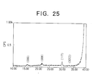
- FIGs. 24 and 25 shown the surface morphology and sectional shape of this Bi 4 Ti 3 O 12 thin-film by perspective SEM photography and the X-ray diffraction pattern of this Bi 4 Ti 3 O 12 thin-film.
- a thin-film according to the fifth embodiment is a good crystallinity Bi 4 Ti 3 O 12 thin-film, so-called random orientation thin-film comprising the c-axis (00n) and (117) oriented components and a dense and smooth thin-film.
- the crystallinity was not so good, use of the present invention enables a Bi 4 Ti 3 O 12 thin-film to be grown even at very low substrate temperature of 300°C.
- a ferroelectric thin-film (Bi 4 Ti 3 O 12 thin-film) exhibiting a good ferroelectric characteristic was obtained at a thin-film forming temperature ranging from 400°C to 650°C for a titanium oxide buffer layer and a growth layer (Bi 4 Ti 3 O 12 thin-film) by the MOCVD process.
- a ferroelectric thin-film (Bi 4 Ti 3 O 12 thin-film) having a strong c-axis orientation and exhibiting a large residual spontaneous polarization Pr was obtained.
- a good ferroelectric characteristic was exhibited at a thin-film forming of a ferroelectric thin-film (Bi 4 Ti 3 O 12 thin-film) by the MOCVD process within the temperature range of 300°C to 400°C.
- the heat treatment in a production method according to the present invention exhibits a significant effect in the temperature range of 500°C to 700°C and a sufficient effect can be obtained for a short period of time even at temperatures around 700°C, so that the present invention is sufficiently applicable also to a highly integrated device.
- conditions of materials, supplied gas or the like except the thin-film forming temperature are not limited to those of the embodiments mentioned above but are appropriately set dependently on a thin-film forming device, supplied gas and the like.
- the thin-film forming temperature of a titanium oxide buffer layer is set equal to that of a Bi 4 Ti 3 O 12 of growth layer considering the productivity, because a change in substrate temperature lengthens the manufacturing time of a device in actual manufacturing steps.
- the thin-film forming temperature of a titanium oxide buffer layer may be set different from that of a Bi 4 Ti 3 O 12 of growth layer.
- FIGs. 26A and 26B show an embodiment wherein to a nonvolatile memory of capacitor structure is made use of the Bi 4 Ti 3 O 12 ferroelectric thin-film mentioned above and the equivalent circuit thereof, respectively.
- a nonvolatile memory of capacitor structure in which use is made of the ferroelectric thin-films shown in these embodiments comprises a capacitor 108 and a transistor 107.
- a capacitor 108 comprises a ⁇ 117> oriented Bi 4 Ti 3 O 12 thin-film 5 and a pair of conductors (electrodes) 110 and 110' sandwiching
- a transistor 107 comprises a bit line 112, a word line 111 and a signal line 113 connected to an AI electrode 109.
- the AI electrode 109 is connected also to the electrode 110' of the capacitor 108.
- a method for producing aforesaid capacitor-structured nonvolatile memory will be described.
- photo-etching is conducted in such a manner that Si 3 N 4 remains at the site on which to form a transistor and field oxidation is effected to form a field SiO 2
- Poly-Si gate 111 is formed.
- a source 112 and a drain 113 are formed by ion implantation with this gate 111 used as a mask, then covering these structures with PSG (silicon phosphate glass) as the interlayer insulating thin-film and making the whole surface even by reflow.
- PSG silicon phosphate glass
- an electrode 110 After forming an electrode 110 thereon, a ⁇ 117> oriented Bi 4 Ti 3 O 12 thin-film 105 and an electrode 110' are formed in sequence. Then, after forming the structures with PSG again and effecting a reflow, contact holes are formed on the electrode 110' and the drain 113 by etching and finally an AI electrode 109 for wiring is provided.
- the ⁇ 117> oriented Bi 4 Ti 3 O 12 thin-film 105 mentioned here is that formed at a thin-film forming temperature of 450°C in the first embodiment mentioned above.
- the ⁇ 117> oriented Bi 4 Ti 3 O 12 thin-film 105 was formed after forming the titanium oxide buffer layer and the growth layer, not shown in FIG. 26A, on the electrode 110 under conditions similar to those of the first embodiment.
- the reason for using a ⁇ 117> oriented Bi 4 Ti 3 O 12 thin-film as the ferroelectric thin-film is that a thin-film exhibiting a large residual spontaneous polarization is preferable in this embodiment.
- the ferroelectric thin-film 105 is polarized and a positive residual polarization charge is stored on the side of the electrode 110 of the capacitor 108.
- this memory device is allowed to operate normally as a DRAM and as a nonvolatile memory only at the OFF period of power supply.
- FIG. 27 shows a sectional structural schematic illustration of this embodiment.
- MFMIS-FET Metal Ferroelectric Metal Insulator Semiconductor-Field Effect Transistor
- the PSG on the PPt gate 115 is removed by etching, a c-axis oriented Bi 4 Ti 3 O 12 ferroelectric thin-film 116 is formed thereon and further a control gate 117 is formed with Pt. Then, after covering these structures with PSG again and effecting a reflow, contact holes are formed on the control gate 117, the drain 119 and the source 120 and finally AI electrodes 118, 121 and 122 for wiring are provided.
- the c-axis oriented Bi 4 Ti 3 O 12 thin-film 116 mentioned here is that formed at a thin-film forming temperature of 500°C for the titanium oxide and the growth layer in the first embodiment mentioned above.
- a c-axis oriented Bi 4 Ti 3 O 12 thin-film 116 was formed after forming the titanium oxide buffer layer and the growth layer not shown in FIG. 27 under conditions similar to those of the first embodiment.
- a c-axis oriented Bi 4 Ti 3 O 12 thin-film is employed as the ferroelectric thin-film.
- the SiO 2 114 of gate insulating is dielectrically polarized via the floating gate 115 by its electrostatic induction and the direction of polarization changes. Since the formation of a channel on the semiconductor surface directly beneath the gate can be controlled by this direction of polarization, "0" and "1" can be defined by the ON-OFF of drain current. That is, assume that, at the zero bias state of the gate electrode, the ferroelectric thin-film 116 is so polarized in the direction of the semiconductor substrate that the side of the floating gate 115 becomes negative. In this case, the SiO 2 114 is dielectrically polarized, its surface in contact with the Si substrate 101 becomes positive, so that the drain 119 and the source 120 are disconnected (OFF state).
- the ferroelectric thin-film 116 inverts the polarization direction and is so polarized that the side of the floating gate 115 becomes positive.
- the SiO 2 114 is dielectrically polarized and its surface in contact with the Si substrate 101 becomes positive, whereas the surface of the Si substrate 101 in contact with the SiO 2 114 becomes negative, so that the drain 119 and the source 120 is connected (ON state). In this state, even when making the gate voltage into a zero bias state, this ON state is maintained by the residual polarization.
- this arrangement can operate as a nonvolatile memory allowing a nondestructive readout.
- a quite excellent ferroelectric characteristic can be obtained in a large value of residual spontaneous polarization and a high reliability can be implemented in excellent leak current characteristic and fatigue resistance.
- a very large value of 16 ⁇ C/cm 2 in residual spontaneous polarization can be obtained and a sufficient ferroelectric characteristic can be obtained even for a approx. 50 nm thick thin-film.
- This advantage enables a sufficient polarization charge to be ensured even when forming a infinitesimal-sized capacitor and accordingly is effective for application to a highly integrated device.
- a very dense and smooth thin-film morphology is obtained, various fine machining processes can be coped with and therefore this advantage is also effective for the application to a highly integrated device.
- a ferroelectric thin-film coated substrate manufacturing method since a ferroelectric thin-film of random orientation thin-film can be obtained and its orientation (crystallinity) can be controlled, the residual spontaneous polarization and the reacting electric field can be controlled dependently on a device to be applied and the degree of freedom can be greatly promoted. And, since the producing step can be carried out at a low temperature, various conventional devices such as a highly integrated device troublesome in high-temperature process can be coped with. Forming a coated thin-film by using the MOCVD process, not a conventional MOD or sol-gel process, enables a large-area thin-film to be produced with a good controllability at high speed, thereby promoting the productivity significantly.
- a capacitor-structured nonvolatile memory according to the present invention permit a sufficient characteristic to be obtained as the nonvolatile memory.
- an MFMIS-FET-structured nonvolatile memory permits a sufficient characteristic to be obtained as the nonvolatile memory.
Description
- The present invention refers to a ferroelectric thin-film coated substrate used in a ferroelectric memory element, a pyroelectric sensor element, a piezoelectric element and the like, and a manufacturing method thereof and the nonvolatile memory comprising a ferroelectric thin-film coated substrate.
- Because of having many functions such as spontaneous polarization, high dielectric constant, electro-optic effect, piezoelectric effect, pyroelectric effect and the like, ferroelectrics are applied to a wide development of devices such as capacitor, oscillator, optical modulator or infrared sensor. So far, for use in these applications, single crystal, such as triglycine sulfate (TGS), LiNbO3 and LiTaO3 or sintered ceramics such as BaTiO3, PbTiO3, Pb(Zr1-x Tix)O3 (PZT) and PLZT, ferroelectric material, has been machined to the order of 50 µm in thickness by cutting and grinding. However, a large size of single crystal is difficult to prepare and expensive, and difficult to machine on account of cleavage. In addition, ceramics are generally fragile and difficult to machine to a thickness of 50 µm or less owing to the occurrence of cracks, so that much labor are required for machining and the cost of production becomes high.
- On the other hand, with an advance in the formation technique of thin-film, the application field of these ferroelectric thin-films widens at present. As one example, applying the characteristic of high dielectric constant to capacitors in various semiconductor elements such as DRAM permits a high integration of elements by downsizing of capacitor area and the reliability promotion thereof. In particular, recently, ferroelectric nonvolatile memories (FRAM) operating in high density and at high speed by combining semiconductor memory elements such as DRAM are extensively developed. Ferroelectric nonvolatile memories need no backup power supply by making use of a ferroelectric characteristic (hysteresis effect) of ferroelectrics. For development of such devices, materials of characteristics such as large residual spontaneous polarization (Pr), small reacting electric field (Ec), low leak current and large repetition resistance of polarization inversion are necessary. Furthermore, for adaptation to a decrease in operating current and the fine machining process of semiconductors, implementation of the above characteristics is desired with a thin-film 200 nm or less in thickness.
- At present, for the purpose of application to FRAM or the like, an attempt is made to make oxide ferroelectrics such as PbTiO3, PZT and PLZT into a thin-film by the thin-film forming method such as sputtering, evaporation, sol-gel process and MOCVD.
- Among the above ferroelectric materials, Pb(Zr1-x Tix) O3 (PZT) is recently being studied most intensively, from which thin-films of good ferroelectric characteristic are obtained by sputtering or sol-gel process. For example, those having as large value of residual spontaneous polarization Pr of 10 to 26µC/cm2 is also obtained. However, there are problems that, although the ferroelectric characteristic of PZT largely depends on the composition x, a change in the composition of a thin-film is apt to occur during thin-film forming or during heat treatment on account of contained Pb having a high vapor pressure and that a leak current and a deteriorated resistance to polarization inversion occur with decreasing thickness of a thin-film (with thinner thin-film) as a result of occurrence of pinholes, occurrence of a low ferroelectric layer due to a reaction of the underlying electrode Pt with Pb. Thus, it is desired to develop other materials excellent in ferroelectric characteristic and resistance to polarization inversion.
- As a material improved in ferroelectric characteristic and excellent in resistance to polarization inversion, Y1 receives much attention. Y1 is a Bi-based layered oxide material, expressed in chemical formula SrBi2 Ta2 O9, and produced by MOD process. The MOD process is a thin-film forming method comprising the following steps. As with the sol-gel process, organic metal materials are mixed to form a predetermined thin-film composition and a material solution for coating with the concentration and the viscosity adjusted is prepared. This solution is spin coated to the ground plate, dried and provisionally sintered. These steps are repeated till the thin-film has reached a predetermined thickness and finally the crystallization by a true sintering is accomplished. Accordingly, control of the thin-film thickness is restricted by the thickness of a one-time coated thin-film (cf. 1994 Autumn Applied Physics Meeting Preprints, 20p-M-19).
- It is most critical in Y1 as ferroelectric material that the sintering temperature is extremely high as 750°C to 800°C and a further long sintering time of an hour or longer is necessary. That is because, when the steps of thin-film formation and heat treatment are performed at 650°C or higher temperatures for a long period of time in such production process, a mutual diffusion reaction between the underlying platinum electrode and ferroelectrics and further a reaction between silicon or silicon oxide below the underlying electrode and ferroelectrics take place, and a change in thin-film composition due to the volatilization of component element from the ferroelectrics thin-film occurs, so that application to the actual production process of devices becomes difficult. For the present, since only a thin-film of as large particle size as 0.3 µm in the surface morphology is obtained, this production process cannot be applied to a submicron-sized fine machining necessary for the development of highly integrated device. Furthermore, since the obtained thin-film is a coating formed thin-film, there are such problems as deterioration of stepped section characteristic and breaking of wire. Thus, though excellent in ferroelectric characteristic and resistance to polarization inversion, Y1 has still a critical problem as ferroelectric material.
- In addition, to implement the integration of ferroelectric nonvolatile memories, use of polycrystalline silicon for wiring between a MOS transistor and a ferroelectric capacitor is examined at present, but preparing a ferroelectrics thin-film such as the above Y1 thin-film in a long-time, high-temperature process has a problem that deterioration of characteristic due to the mutual diffusion between a polycrystalline silicon for wiring and a ferroelectric capacitor takes place. To solve such a problem, various structures with the diffusion barrier inserted are examined, but the tolerance of thin-film forming temperature is up to 650°C and 700°C is considered to be the limit also for other heat treatment steps if the process needs only a short time. However with the above Y1 or other dielectric thin-film under present circumstances, since not only crystallinity but also ferroelectric characteristic generally increases with higher thin-film forming temperature, the crystallinity and the ferroelectric characteristic deteriorate for lower thin-film forming temperature, so that compatibility between promoted dielectric characteristic and low-temperature thin-film forming is difficult.
- On the other hand, oxide ferroelectrics not containing Pb adversely affecting the leak current and resistance to polarization inversion include a group of bismuth based oxide ferroelectrics having layered crystal structures expressed in the following general chemical formula.
- Here, A is selected from Na1+, K1+, Pb2+, Ca2+, Sr2+, Ba2+, Bi3+ and the like, B is selected from Fe3+, Ti4+, Nb5+, Ta5+, W6+ and Mo6+, and m is an integer not less than 1. Their crystal structure have a fundamental structure in which a layered perovskite layer in an array of perovskite lattices composed of (m-1) ABO3 is sandwiched by two layers of (Bi2 O2)2+ from above and from below. Among these, many combinations of Sr, Ba or Bi as A with Ti, Ta or Nb as B exhibit ferroelectricity. The above Y1 is one type of these bismuth based oxide ferroelectrics.
- Even among ferroelectrics expressed in the above chemical formulae, Bi4 Ti3 O12 (bismuth titanate) is a ferroelectric having a strongly anisotropic layered perovskite structure (rhombic system/lattice constants: a=5.411 angstrom, b=5.448 angstrom and c=32.83 angstrom) and the ferroelectricity of its single crystal has the largest spontaneous polarization as indicated by Pr=50µC/cm2 and Ec=50kV/cm in the a-axis direction and exhibits a surpassing characteristic. Thus, for applying a large spontaneous polarization inherent in this Bi4 Ti3 O12 to ferroelectric nonvolatile memories and the like, it is desirable to arrange the a-axis component of more crystals perpendicularly to the surface of a substrate.
- Attempts have thus far been made to make Bi4 Ti3 O12 into a thinner thin-film by the MOCVD method and the sol-gel method, but almost all of these attempts relate to a c-axis orientation thin-film less in spontaneous polarization than a-axis orientation thin-film. In addition, with a conventional sol-gel method, since the heat treatment at above 650°C is necessary for obtaining a good ferroelectric characteristic and further the thin-film surface morphology comprises crystal grains on the order of 0.5 µm, application to a highly integrated device requiring the fine machining is difficult. On the other hand, with the MOCVD method, a c-axis oriented Bi4 Ti3 O12 thin-film is prepared at substrate temperatures of 600°C or higher on a Pt/SiO2/Si substrate or on a Pt substrate, but these substrates cannot be directly applied to an actual device structure. That is, as with the Pt/Ti/SiO2/Si substrate, an adhesive layer, such as Ti layer, for ensuring the adhesive strength between the Pt electrode layer and its underlying SiO2 layer is necessary. Nevertheless, it was reported that, when preparing a thin Bi4 Ti3 O12 thin-film on the Pt electrode layer provided with such an adhesive layer by the MOCVD process, its thin-film surface morphology comprises coarse crystal grains and moreover the Pyrochlore phase (Bi2 Ti2 O7) becomes apt to occur (cf. Jpn. J. Appl. Phys., 32, 1993, pp. 4086 and J. Ceramic Soc. Japan, 102, 1994, pp. 512). The former reference discloses a Bi4 Ti3 O12 ferroelectric thin film deposited on a buffer layer of Bi2 Ti2 O7. When the thin-film surface morphology comprises coarse crystal grains, application to a highly integrated device requiring a fine machining is impossible and moreover pin holes are still more apt to be caused for the thinner thin-film and consequently occurrence of leak current is induced. In addition, since the pyrochlore phase exhibits no ferroelectricity, mixing of the pyrochlore phase leads to deterioration of ferroelectricity on the whole thin-film. Thus, under such circumstances of conventional art, it is difficult to implement a ferroelectric thin-film, 200 nm thick or thinner, having a good ferroelectric characteristic.
- As described above, the above prior art has a problem that, in applying a ferroelectric thin-film to highly integrated devices, those satisfactorily meeting the denseness and the evenness of the surface of a thin-film required for fine machining or low leak current, a large residual spontaneous polarization, and various requirements for the low-temperature thin-film forming process are not yet obtained.
- For solving the problem mentioned above, it is desirable to provide a ferroelectric substrate having a dense and even surface and a large residual spontaneous polarization which can be prepared in the low-temperature thin-film forming process, and the manufacture method thereof, and a nonvolatile memory composed thereof.
- The present invention provides a ferroelectric thin-film coated substrate as set out in claim 1.
- The layered crystal structure expressed in a chemical formula Bi2 Am-1 Bm O3m+3, where A is selected from Na1+, K1+, Pb2+, Ca2+, Sr2+, Ba2+, Bi3+ and the like, B is selected from Fe3+, Ti4+, Nb5+, Ta5+, W6+ and Mo6+, and m is an integer not less than 1, is a crystal structure formed by the alternate stacking of (Bi2 O2)2+ layers and (Am-1 Bm O3m+3)2- layers.
Incidentally, selection of A and B here is not limited to a single way. - Typical of ferroelectric materials having such a crystal structure is Bi4 Ti3 O12. And, others are SrBi2 Nb2 O9, SrBi2 Ta2 O9, Babi2 Nb2 O9, BaBi2 Ta2 O9, Pb2 Bi2 Nb2 O9, PbBi2 Ta2 O9, SrBi4 Ti4 O15, BaBi4 Ti4 O15, PbBi4 Ti4 O15, Na0.5 Bi4.5 Ti4 O15, K0.5 Bi4.5 Ti4 O15, Sr2 Bi4 Ti5 O18, Ba2 Bi4 Ti5 O18 and Pb2 Bi4 Ti5 O18. In contrast to these, ferroelectric materials expressed in the same chemical formula, having a layered crystal structure and exhibiting no ferroelectric characteristic include Bi3 TiNbO9, Bi3 TiTaO9, CaBi2 Nb2 O9, CaBi2 Ta2 O9 and CaBi4 Ti4 O15.
- Ferroelectric thin-film coated substrates made by forming ferroelectric thin-films composed of these bismuth-based oxide ferroelectric materials on a substrate, the interposition of both a buffer layer and a growth layer for allowing the ferroelectric thin-film to grow between the substrate and the ferroelectric thin-film enables a marked upgrade in crystallinity, ferroelectricity, electrical properties, thin-film properties and the like.
- The detail will be described later, but such operations of embodiments of the present invention was examined using a ferroelectric thin-film of Bi4 Ti3 O12, representative of the above ferroelectric materials, and employing a Bi4 Ti3 O12 thin-film as the growth layer and a titanium oxide thin-film as the buffer layer. As a result, it was firstly found that the ferroelectric thin-film formed a random orientation thin-film. According to this random orientation thin-film, since use can be made of the a-axis orientated component unlike a formerly reported c-axis oriented thin-film made of Bi4 Ti3 O12 ferroelectric, the residual spontaneous polarization of a ferroelectric thin-film can be greatly promoted.
- Secondly, it was found in the thin-film surface of a Bi4 Ti3 O12 ferroelectric thin-film according to an embodiment of the present invention that no such c-plane platelike coarse crystalline grain as present in a conventional Bi4 Ti3 O12 ferroelectric thin-film was seen, very fine crystalline grains were observed and a very dense and smooth thin-film surface morphology was obtained. Thus, in a ferroelectric thin-film according to an embodiment of the present invention, since no leak current is generated by pinholes originating in composition of coarse crystalline grains, a highly low leak current characteristic can be manifested and further the fatigue resistance can also be greatly promoted. Since an excellent thin-film surface morphology is exhibited in this way, a fine machining is enabled and the present invention is applicable to a highly integrated device.
- It is attributable to the buffer layer and the growth layer that a very good bismuth-based ferroelectric thin-film can be obtained like this according to the present invention. From an observation of the thin-film surface and the crystallinity of the growth layer (Bi4 Ti3 O12 thin-film) formed on the titanium oxide buffer layer, it is considered that the surface morphology and the crystallinity of a ferroelectric thin-film becomes equivalent to those of the growth layer as if succeeded to them.
- From such results, the present invention can be thought to be effective for those dielectric materials expressed in the above-mentioned chemical formula Bi2 Am-1 Bm O3m+3 having a layered crystal structure similar to that of a Bi4 Ti3 O12 as the ferroelectric thin-film. In addition, as the growth layer, since those indicating a crystal structure resembling that of a ferroelectric thin-film is thought to be preferable, those composed of oxide materials containing the component elements of a ferroelectric thin-film or bismuth-based oxide materials having a layered structure similar to that of a ferroelectric thin-film can be regarded as preferable. Furthermore, as for the buffer layer, those composed of the component elements of the ferroelectric thin-film and the growth layer can be regarded as preferable.
- The invention also provides a method for manufacturing a ferroelectric thin film coated substrate as set out in claim 4.
- The invention further provides a method for manufacturing a ferroelectric thin-film coated substrate as set out in claim 8.
- The detail will be described in the preferred arrangement, but a method for manufacturing a ferroelectric thin-film coated substrate according to an embodiment of the present invention was examined employing a ferroelectric thin-film of Bi4 Ti3 O12, representative of the above ferroelectric materials, and forming a Bi4 Ti3 O12 thin-film as the growth layer and a titanium oxide thin-film as the buffer layer.
- As a result, it was found that a random orientation thin-film of Bi4 Ti3 O12 ferroelectric thin-film could be formed by forming a growth layer (Bi4 Ti3 O12 thin-film) at thin-film forming temperatures of 400°C to 650°C and a Bi4 Ti3 O12 ferroelectric thin-film at lower temperatures of 300°C to 400°C than the growth layer forming temperature. Furthermore, by controlling the thin-film forming temperature of the growth layer (Bi4 Ti3 O12 thin-film) within the range of 400°C to 650°C, the crystallinity (orientation) of a ferroelectric thin-film was found to be controllable. This control is possible because, by intensifying either one of the random oriented component and the c-axis oriented component in the oriented components in a Bi4 Ti3 O12 ferroelectric thin-film of random orientation thin-film, the residual spontaneous polarization of the ferroelectric thin-film can be increased or the reacting electric field can be decreased. Thus, corresponding to an actually applying device, an appropriate characteristic of ferroelectric thin-films can be freely selected, thereby promoting the degree of freedom greatly.
- Furthermore, with the manufacturing method according to an embodiment of the present invention, since a Bi4 Ti3 O12 ferroelectric thin-film can be formed at by far lower temperatures of 300°C to 400°C than the conventional thin-film forming temperature, a very dense and smooth thin-film can be implemented. In addition, because the above thin-film forming process can be performed at the temperature of 650°C or less, it is very effectively applied to a highly integrated device.
- By setting the thin-film forming temperature of the above growth layer (Bi4 Ti3 O12 thin-film) in the range of 400°C to 470°C, the randomly oriented component can be intensified and the residual spontaneous polarization of a ferroelectric thin-film can be very greatly increased as compared with a conventional one by effectively utilizing the a-axis oriented component of Bi4 Ti3 O12.
- Furthermore, by applying the heat treatment step after such a thin-film forming step as mentioned above, the crystallinity of a ferroelectric thin-film can be further enhanced, the residual spontaneous polarization can be increased and the leak current characteristic can be noticeably improved. For a Bi4 Ti3 O12 ferroelectric thin-film, the heat treatment temperature is effective in the range of 500°C to 700°C, and since the effect is obtained by a short-time treatment even around 700°C, no adverse effect is exerted even on a highly integrated device in application.
- Because of comprising the above-mentioned ferroelectric thin-film coated substrate, capacitor-structured nonvolatile memories according to the present invention can exhibit a sufficient characteristic.
- Because of comprising the above-mentioned ferroelectric thin-film coated substrate, MFMIS-FET-structured nonvolatile memories according to the present invention can exhibit a sufficient characteristic.
- Further objects and advantages of the present invention will be apparent from the following description of the preferred embodiments of the present invention as illustrated in the accompanying drawings.
-
- FIG. 1 is a sectional schematic view showing the structure of a ferroelectric thin-film coated substrate according to an embodiment of the present invention;
- FIGs. 2A and 2B are photographs showing the SEM observed results of the surface of a first embodiment of Bi4 Ti3 O12 thin-film (growth layer);
- FIG. 3 is a photograph showing the SEM observed result of the surface of a control of Bi4 Ti3 O12 thin-film;
- FIGs. 4A and 4B are graphs showing the X-ray diffraction observed results of the surface of a Bi4 Ti3 O12 thin-film (growth layer) of a first embodiment;
- FIG. 5 is a graph showing the X-ray diffraction observed result of the crystallinity of a control of Bi4 Ti3 O12 thin-film;
- FIGs. 6A and 6B are photographs showing the SEM observed results of the surface of a Bi4 Ti3 O12 ferroelectric thin-film of a first embodiment;
- FIGs. 7A and 7B are graphs showing the X-ray diffraction observed results of the crystallinity of Bi4 Ti3 O12 ferroelectric thin-film of a first embodiment;
- FIG. 8 is a graph showing a ferroelectric hysteresis curve of a first embodiment;
- FIG. 9 is a graph showing the applied-voltage dependence of leak current (I1) of a first embodiment;
- FIG. 10 is a graph showing a ferroelectric hysteresis curve of a first embodiment;
- FIG. 11 is a graph showing a ferroelectric hysteresis curve of a second embodiment;
- FIG. 12 is a graph showing the repetition times dependence of switching charge quantity of a second embodiment;
- FIG. 13 is a photograph showing the SEM observed result of the surface of a second embodiment of a Bi4 Ti3 O12 ferroelectric thin-film of a second embodiment;
- FIG. 14 is a graph showing the applied-voltage dependence of leak current (I1) of a third embodiment;
- FIG. 15 is a photograph showing the SEM observed result of the surface of a Bi4 Ti3 O12 ferroelectric thin-film of a fourth embodiment;
- FIG. 16 is a graph showing a ferroelectric hysteresis curve of a fourth embodiment;
- FIG. 17 is a photograph showing the SEM perspective observation result of the surface of a Bi4 Ti3 O12 ferroelectric thin-film of a fifth embodiment;
- FIG. 18 is a graph showing the X-ray diffraction observed result of the crystallinity of a Bi4 Ti3 O12 ferroelectric thin-film of a fifth embodiment;
- FIG. 19 is a graph showing a ferroelectric hysteresis curve of a fifth embodiment;
- FIG. 20 is a graph showing the applied-voltage dependence of leak current (I1) of a fifth embodiment;
- FIG. 21 is a graph showing the repetition times dependence of switching charge quantity and the comparison of ferroelectric hysteresis curves before and after the repetition (1012 cycles) of a fifth embodiment;
- FIG. 22 is a photograph showing the SEM perspective observation result of the surface of a Bi4 Ti3 O12 ferroelectric thin-film of a sixth embodiment;
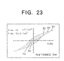
- FIG. 23 is a graph showing a ferroelectric hysteresis curve of a sixth embodiment;
- FIG. 24 is a photograph showing the SEM perspective observation result of the surface of a ferroelectric thin-film of a seventh embodiment;
- FIG. 25 is a graph showing the X-ray diffraction observed result of the crystallinity of a Bi4 Ti3 O12 ferroelectric thin-film of a seventh embodiment;
- FIGs. 26A and 26B are schematic views showing the sectional structure and an equivalent circuit diagram of capacitor-structured nonvolatile memory using a Bi4 Ti3 O12 ferroelectric thin-film according to an embodiment of the present invention; and
- FIG. 27 is a schematic view showing the sectional structure of MFMIS-FET using a Bi4 Ti3 O12 ferroelectric thin-film according to an embodiment of the present invention.
-
- Hereinafter, the preferred embodiments of the present invention will be described referring to the drawings.
- FIG. 1 shows the structure of a ferroelectrics thin-film substrate according to a first embodiment of the present invention. As shown in FIG. 1, this ferroelectric thin-film coated substrate comprises a silicon oxide (SiO2) layer 2, an adhesive layer 3, a lower electrode layer 4, a buffer layer 5, c growth layer for allowing a ferroelectrics thin-film to grow 6, a ferroelectric thin-film 7 and an upper electrode layer 8 successively formed on a silicon (Si) substrate 1.
- With the first embodiment, a silicon single crystal wafer was employed as the silicon substrate 1, while a silicon oxide thin-film obtained by thermally oxidizing the surface of the silicon single crystal wafer was employed as the SiO2 layer 2. In addition, a tantalum (Ta) thin-film, a platinum (Pt) thin-film, a titanium oxide thin-film, a Bi4 Ti3 O12 thin-film, a Bi4 Ti3 O12 thin-film and a platinum (Pt) thin-film are employed as the adhesive layer 3, the lower electrode layer 4, a buffer layer 5, a growth layer 6, a ferroelectric thin-film 7 and an upper electrode layer 8, respectively.
- Next, the method for producing a ferroelectrics thin-film coated substrate according to the first embodiment shown in FIG. 1 will be described.
- First, preparation of a Pt/Ta/SiO2/Si substrate will be described. By thermal oxidation of the surface of (100) plane in a silicon single crystal wafer as the silicon substrate 1, a SiO2 layer 2, 200 nm in thin-film thickness, is formed. Then, a Ta thin-film as the adhesive layer 3, 30 nm in thin-film thickness, and a Pt thin-film as the lower electrode layer 4, 200 nm in thin-film thickness, are formed respectively by the sputter method.
- Here, these materials and the thin-film thickness are not limited to this arrangement, but a polycrystalline silicon substrate, a GaAs substrate or the like may be also employed. In addition, the adhesive layer is provided for preventing the peeling of a thin-film from occurring during the thin-film forming due to a difference in thermal expansion coefficient between the substrate and the lower electrode layer, the thin-film thickness is only necessary to be as thick as capable of preventing the peeling of a thin-film. Other materials such as titanium (Ti) than Ta may be employed, but Ta is preferable because Ti and Pt form an alloy. The SiO2 layer employed for the insulating layer may not be prepared by heat treatment, an SiO2 thin-film, a silicon nitride thin-film or the like are formed by the sputtering process, the vapor deposition process and the like. Any material and any thin-film thickness are allowable so long as a sufficient insulation is ensured.
- Similarly, with respect to the lower electrode layer, the thin-film thickness is only required to be as large as equal to the function of an electrode and the material is not limited to Pt but may be metal materials employed for ordinary electrode materials and can be appropriately selected in relation to other thin-film. In addition, a thin-film formation method is also not limited to the silicon oxidation process or the sputtering process heretofore and ordinary thin-film forming techniques such as vapor deposition may be employed. Furthermore, the structure of a substrate is also not limited to the above-mentioned.
- Then, after forming a titanium oxide thin-film of buffer layer and a Bi4 Ti3 O12 thin-film of growth layer by the MOCVD process on the Pt/Ta/SiO2/Si substrate prepared in this manner, the surface morphology and the orientation were observed for varied thin-film forming conditions of the growth layer.
- For the thin-film formation of a titanium oxide of buffer layer, titanium isopropoxide (Ti(i-OC3 H7)4) was used as a raw material for titanium, heated to 50°C, gasified and supplied into a thin-film forming chamber together with argon (Ar) gas of carrier gas. Here, the flow rate at the Ar gas supply was set at 100 sccm. And with Pt/Ta/SiO2/Si substrate prepared as described above heated and kept at a definite temperature in the thin-film forming chamber, a 5 nm thick titanium oxide thin-film was formed on this substrate. At that time, the time taken for the forming step of a titanium oxide was of the order of 30 sec.
- Thereafter, a Bi4 Ti3 O12 thin-film of growth layer is continuously formed in a thickness of 45 nm on this titanium oxide thin-film at the same temperature. Table 1 shows the supply conditions of raw materials for the thin-film forming by the MOCVD process at this time.
Raw material Bi(o - C7H7)3 Ti(i - OC3H7)4 Raw material temperature 160°C 50°C Carrier gas (Ar) flow rate 200 sccm 100 sccm Reactant gas (O2) flow rate 1000 sccm Reaction pressure 666 Pa (5 Torr) - As shown in Table 1 using triorthotolylbiryl bismuth (Bi(o-OC7 H7)3) and titanium isopropoxide (Ti (i-OC3 H7)4) as raw materials for bismuth and titanium, respectively for forming a Bi4 Ti3 O12 thin-film, these raw materials were heated and gasified at respective raw material temperatures shown in Table 1 (160°C for bismuth raw material and 50°C for titanium raw material) and supplied into the thin-film forming chamber together with a carrier gas of argon (Ar) gas and a reactant gas of oxygen (O2). Here, the flow rate of Ar gas at the supply was set at 200 sccm for Bi raw material and 100 sccm for Ti raw material, while the flow rate of O2 gas at the supply was set at 1000 sccm. Incidentally, in these thin-film forming steps, the degree of vacuum in the thin-film forming chamber was set at 5 Torr, because the gaseous phase reaction is apt to occur if it is above 1333 Pa (10 Torr).
- Here, setting the thin-film forming temperature, i.e., the substrate temperature at 450°C and 500°C, two kinds of samples, 50 nm in the total thickness of a titanium oxide buffer layer and a Bi4 Ti3 O12 thin-film (growth layer), were prepared. The thin-film thickness of Bi4 Ti3 O12 thin-film (growth layer) here was set at 45 nm, and was made rather larger at any rate for purposes of observing the surface morphology and the crystallinity.
- In addition, for comparison, a control was also prepared in which no titanium oxide buffer layer was formed and a Bi4 Ti3 O12 thin-film was formed directly on the Pt/Ta/SiO2/Si substrate in a thickness of 150 nm. Except that no titanium oxide buffer layer was formed and the thin-film forming temperature was set at 500°C, the thin-film forming conditions for this control are quite the same as with the samples mentioned above.
- For the two sorts of samples having a titanium oxide buffer layer and the control prepared in this manner, observation of the surface morphology under SEM (Scanning Electron Microscope) and observation of the crystallinity on X-ray diffractometer were carried out. At this time, FIGs. 2A, 2B and 3 show the SEM observed results, while Figs 4A, 4B and 5 shows the observed results on X-ray diffractometer. In the thin-film forming temperature (substrate temperature), FIGs. 2A and 4A relate to samples of 450°C and FIGs. 2B and 4B relate to samples of 500°C, respectively. FIGs. 3 and 5 show the respective observed results of controls without titanium oxide buffer layer.
- According to the SEM photos of FIGs. 2A and 2B, it is found that samples with the titanium oxide buffer layer formed exhibit a very dense and smooth thin-film surface morphology with crystalline grains on the order of nm and on the order of 10 nm respectively for FIG. 2A sample and for FIG. 2B sample. This becomes clear if compared with the result of the control without titanium oxide buffer layer shown in FIG. 3 that exhibits a rough uneven surface morphology of platelike coarse crystalline grains (µm order) formed. In FIG. 2A, a circularly blackened portion is seen in part, but it is a burn generated by electron irradiation during the SEM observation and does not represent a defect or the like on the surface of a thin-film.
- In FIGs. 4A, 4B and 5, all diffraction peaks but the Pt (111) peak are attributed to the Bi4 Ti3 O12. (00n) (n: integer) denotes the c-axis orientation, (n00) denotes the a-axis orientation, the others such as (117) denotes random orientations. Accordingly, according to FIGs. 4A and 4B, the sample of FIG. 4A, having a large diffraction peak of (117), small c-axis oriented diffraction peaks of (006) and (008), and a small a-axis oriented diffraction peaks of (200), is found to be randomly oriented. As compared with that of FIG. 4A, the sample of FIG. 4B, having a smaller diffraction peak of (117), larger c-axis oriented diffraction peaks of (006) and (008), is found to be more oriented in c-axis. Meanwhile, in FIG. 5, only c-axis oriented diffraction peaks of (00n) (n: integer) are indicated and therefore the control exhibits the c-axis orientation containing no random orientation.
- In this way, it was found from these results of SEM and X-ray diffraction observation that samples with the titanium oxide buffer layer formed exhibit a very dense, smooth and good thin-film surface morphology and forms a random orientation thin-film containing components other than that of the c-axis orientation. Furthermore, it was found that those of 450°C in the thin-film forming temperature (substrate temperature) of the titanium oxide buffer layer and the Bi4 Ti3 O12 thin-film exhibit a denser and smoother surface morphology than those of 500°C and are superior in random orientation for crystallinity.
- Now, preparation of a structure having a titanium oxide buffer layer, a Bi4 Ti3 O12 thin-film of growth layer and a Bi4 Ti3 O12 thin-film of ferroelectric thin-film successively formed on a Pt/Ta/SiO2/Si substrate will be described.
- The thin-film forming up to the Bi4 Ti3 O12 thin-film of growth layer is carried out in quite the same manner as that described above except for setting the thickness of a Bi4 Ti3 O12 thin-film of growth layer to 5 nm. Also in this case, two types of samples were prepared setting the thin-film forming temperature (the substrate temperature) of a Bi4 Ti3 O12 thin-film (growth layer) at 450°C and 500°C. The time taken for the thin-film forming step of a Bi4 Ti3 O12 thin-film growth layer was around 30 sec for any sample.
- After the forming procedure up to the forming of a Bi4 Ti3 O12 thin-film (growth layer) was accomplished in the same manner as described above, the supply of raw materials was once ceased. After setting the substrate temperature at 400°C, a Bi raw material, a Ti raw material, a carrier gas (Ar) and a reactant gas (O2) are supplied again into the thin-film forming chamber, and the thin-film forming of a Bi4 Ti3 O12 of ferroelectric thin-film was carried out in a thickness of 90 nm by the MOCVD process with the degree of vacuum in the thin-film forming chamber set at 666 Pa (5 Torr). Here, except for the substrate temperature (thin-film forming temperature), the thin-film forming conditions for a Bi4 Ti3 O12 of ferroelectric thin-film are quite the same as those of a Bi4 Ti3 O12 thin-film of growth layer described using Table 1. At this time, the time taken for the thin-film forming step of a Bi4 Ti3 O12 thin-film of ferroelectric thin-film was around 30 min for any sample, and therefore the time taken for the thin-film forming step of a buffer layer, a growth layer and a ferroelectric thin-film is nearly equal to 30 min in total for any sample.
- Here, for the Bi4 Ti3 O12 thin-film of ferroelectric thin-film formed on the Pt/Ta/SiO2/Si substrate via the titanium oxide buffer layer and the Bi4 Ti3 O12 thin-film of growth layer in this manner, the results obtained by the observation of the surface morphology under SEM (Scanning Electron Microscope) and observation of the crystallinity on X-ray diffractometer will be described.
- FIGs. 6A and 6B show the observed results under SEM, while FIGs. 7A and 7B show the observed results on X-ray diffractometer. In thin-film forming temperature (substrate temperature) of a growth layer, FIGs. 6A and 7A relate to samples of 450°C and FIGs. 6B and 7B relate to samples of 500°C.
- According to the SEM photos of FIGs. 6A and 6B, it is found that samples exhibit a very dense and smooth thin-film surface morphology with crystalline grains on the order of nm and on the order of 10 nm respectively for FIG. 6A and FIG. 6B. This becomes clear if compared with the result not shown of the control without titanium oxide buffer layer that exhibits a rough uneven surface morphology of platelike coarse crystalline grains (µm order) formed. It was found from these observed results of surface morphology that the surface morphology of a Bi4 Ti3 O12 thin-film of ferroelectric thin-film is evidently affected strongly by that of a Bi4 Ti3 O12 thin-film of growth layer and forms a nearly equivalent surface morphology.
- In addition, as regards crystallinity, it is found from the results of X-ray diffraction in FIGs. 7A and 7B that, as with the thin-film surface morphology, the crystallinity of a Bi4 Ti3 O12 thin-film of ferroelectric thin-film is evidently affected strongly by that of a Bi4 Ti3 O12 thin-film of growth layer and exhibits a nearly equivalent orientation.
- Incidentally, this arrangement showed only the results for the thin-film forming temperature of the growth layer of 450°C and for that of 500°C, but it could be confirmed that the thin-film forming temperature ranging from 400°C to 650°C permits a sufficiently smooth and dense crystallinity of growth layer (Bi4 Ti3 O12 thin-film) to be obtained. Furthermore, at thin-film forming temperature of not lower than 650°C, though the crystallinity is high, the growth of crystalline grains was so much that no smooth-surface growth layer (Bi4 Ti3 O12 thin-film) could be obtained.
- As described above, it was found from these results of SEM and X-ray diffraction observation that a Bi4 Ti3 O12 of ferroelectric thin-film according to an embodiment of the present invention exhibits a very dense, smooth and good thin-film surface morphology and forms a random orientation thin-film containing components other than that of the c-axis orientation. Furthermore, it was found that those of 450°C in the thin-film forming temperature (substrate temperature) of the Bi4 Ti3 O12 thin-film exhibit a denser and smoother surface morphology than those of 500°C and are superior in random orientation regarding crystallinity.
- Then, such a capacitor structure as shown in FIG. 1 was constructed by forming an upper electrode layer on the ferroelectric thin-film (Bi4 Ti3 O12 thin-film) for two types of samples prepared in this manner and the electric characteristic of this thin-film was estimated, where a 100 µm Pt electrode thin-film was formed as this electrode by vacuum deposition process. As a result of estimating ferroelectric characteristic with voltage applied between the lower electrode layer 1 and the upper electrode layer 8 shown in FIG. 1, a sample with the growth layer (Bi4 Ti3 O12 thin-film) formed at 450°C exhibits such a ferroelectric hysteresis curve as shown in FIG. 8. That is, in a sample with the growth layer (Bi4 Ti3 O12 thin-film) formed at 450°C, the residual spontaneous polarization Pr=16µC/cm2 and reacting electric field Ec=135kV/cm was obtained under application of 5V. This Pr indicates a by far larger value than the value of Pr=4µC/cm2 in the c-axis direction reported for a Bi4 Ti3 O12 single crystal.
- Since the a-axis value of Pr in Bi4 Ti3 O12 is known to be larger than the c-axis value and the crystallinity of this arrangement exhibits a random orientation, such a large value of Pr in this arrangement as 16µC/cm2 is attributable to a large contribution of the a-axis oriented component in a Bi4 Ti3 O12 thin-film.
- In this sample, as a result of measuring a leak current I1, the applied voltage dependence is found as shown in FIG. 9 and a small good value of I1=7×10⁻⁹A/cm2 is obtained at an applied voltage of 5V. The reason for this small leak current can be considered as follows. Since mm-sized platelike coarse crystalline grains (c-plane crystalline grains) as shown in FIG. 3, found in the thin-film surface observation of a control formed without titanium oxide buffer layer, was present in a conventional Bi4 Ti3 O12 ferroelectric thin-film, a leak current due to pinholes is apt to occur. In this arrangement, however, since the growth of crystalline grains is suppressed by low-temperature thin-film forming and a thin-film structure composed of fine crystalline grains is formed as shown in FIG. 2, the occurrence of conventional pinholes is suppressed and a low leak current value is considered to be obtained.
- FIG. 10 shows the ferroelectric hysteresis curve of a still another sample of this arrangement, i.e., a sample with the growth layer (Bi4 Ti3 O12 thin-film) formed at 500°C. As shown in FIG. 10, this sample exhibited a residual spontaneous polarization Pr=2µC/cm2 and a reacting electric field Ec=50kV/cm. This Pr is smaller than Pr of FIG. 8, and Ec is also smaller than Ec of FIG. 8. This is attributable to a strong c-axis oriented component though the crystallinity of this sample is a random orientation. Such a small value of Ec suggests that the sample is applicable to a device operable at low voltage. Also in this sample, as small good a value of leak current was obtained as I1=1×10⁻⁸A/cm2.
- As described above, it was found that, according to this arrangement, any sample with a Bi4 Ti3 O12 thin-film of growth layer formed at 450°C and at 500°C exhibited a very dense, smooth and good thin-film surface morphology in a Bi4 Ti3 O12 thin-film of ferroelectric thin-film and formed a random orientation thin-film containing components other than that of c-axis orientation. Furthermore, a good ferroelectric characteristic is exhibited in any sample, and especially in a sample with the Bi4 Ti3 O12 thin-film of growth layer formed at 450°C, a very large value of Pr was obtained as seen in Pr=16µC/cm2.
- Though this embodiment showed only the result of those whose thin-film forming temperature for the ferroelectric thin-film is 400°C, it was found that the ferroelectric thin-film can sufficiently succeed to the crystallinity and the surface morphology of the lower electrode layer if its thin-film forming temperature is 300°C or higher. However, the case of thin-film forming temperature of 400°C is superior in ferroelectric characteristic.
- Next, a second embodiment, having a thinner Bi4 Ti3 O12 thin-film of ferroelectrics thin-film than that of the first embodiment, will be described. With this embodiment, the thin-film forming temperature of a Bi4 Ti3 O12 of growth layer was set at 450°C, a sample having a 40 nm thick Bi4 Ti3 O12 of ferroelectric thin-film and having a 50 nm thick composite of titanium oxide buffer layer and growth layer was prepared. Except that the thickness of a Bi4 Ti3 O12 of ferroelectric thin-film was set at 40 nm, the preparing method was quite the same as with the first embodiment. At that time, the time taken for the step of forming a Bi4 Ti3 O12 ferroelectric thin-film was around 15 min and therefore the time taken for the steps of forming a buffer layer, a growth layer and ferroelectric layer is approximately 15 min in total.
- The ferroelectric hysteresis curve of a sample according to this embodiment obtained from a measurement similar to that of the first embodiment is shown in FIG. 11. As clearly seen from FIG. 11, though the ferroelectric thin-film, 40 nm thick, was very thin, a very good ferroelectric characteristic was obtained as indicated by the residual spontaneous polarization Pr=4.5µC and the reacting electric field Ec=139kV for a low applied voltage of 3V. On measuring the leak current, a low value of I1=5×10⁻⁶ was obtained in spite of as thick a ferroelectric thin-film as 40 nm.
- Furthermore, the repetitive fatigue for polarization inversion was measured on a sample according to this embodiment The test conditions are that, when repeatedly applying a pair of bipolar pulses at an applied voltage of 3V and in a pulse width of 100 ns, the changing rate of switching charge quantity (difference between the inversion charge quantity and the non-inversion charge quantity of polarization) is measured. The results are shown in FIG. 12. As shown in FIG. 12, a decrease in switching charge quantity is about 13% after 1 × 10¹² times of repetitions and accordingly the fatigue resistance of this arrangement is clearly by far superior since that of a conventional PZT material is at most on the order of 108.
- FIG. 13 shows the observed results of thin-film surface morphology under SEM in this arrangement. Since the thin-film is thin, this sample comprises fine crystalline grains on the order of nm and a good characteristic of very dense and smooth thin-film was found to be obtained.
- A third embodiment with heat treatment applied to a sample prepared according to the second embodiment will be described. As conditions for heat treatment, the RTA (Rapid Thermal Annealing), high-speed heat treatment by infrared irradiation, was applied at a heat treatment temperature of 650°C in oxygen gas flow and the ferroelectric characteristic was examined for different periods of treatment time of 2 min, 10 min and 30 min. As a result, the residual spontaneous polarization Pr was Pr=4.8µC/cm for 2 min treatment time, Pr=5.9µC/cm for 10 min treatment time and Pr=7.1µC/cm for 30 min. With longer RTA treatment time Pr is remarkably improved.
- Furthermore, leak current Il varies depending on applied voltage as shown in FIG.14. When 3V is applied, Il was Il=8×10⁻⁸ A/cm2 for 2 min treatment time, Il=2X10⁻⁸ A/cm2 for 10 min treatment time and Il=2X10⁻⁹ A/cm2 for 30 min treatment time. With longer RTA treatment time, Il was markedly improved. This is attributable to an improvement in the crystallinity of a Bi4 Ti3 O12 of ferroelectric thin-film due to heat treatment in this arrangement.
- As a fourth embodiment, a sample having a 190 nm thick Bi4 Ti3 O12 ferroelectric thin-film and having a 200 nm composite of titanium oxide buffer layer and growth layer (Bi4 Ti3 O12) was prepared. Except that the thin-film forming temperature of a growth layer (Bi4 Ti3 O12 thin-film) was set at 450°C, the preparing method was quite the same as that of the first and second embodiments. At that time, the time taken for the step of forming a Bi4 Ti3 O12 ferroelectric thin-film was of the order of 60 min and therefore the time taken for the steps of forming a buffer layer, a growth layer and ferroelectrics layer is approximately of the order of an hour in total.
- FIG. 15 shows the result of SEM observation of thin-film surface morphology in this embodiment. As clearly seen from the SEM photo of FIG. 15, a very dense, smooth and good thin-film surface morphology on the order of 10 nm is exhibited. Although the thin-film thickness was nearly double that of the first embodiment, the surface morphology of the Bi4 Ti3 O12 ferroelectric thin-film is found to be strongly affected by the growth layer (Bi4 Ti3 O12 thin-film).
- FIG. 16 shows the ferroelectric hysteresis curve of a sample according to this embodiment, measured as with the above embodiments. As shown in FIG. 16, the residual spontaneous polarization and the resisting electric field are obtained as Pr=14µC/cm2 and Ec=180kV/cm in this arrangement. Still in this embodiment, since the Bi4 Ti3 O12 ferroelectric thin-film forms a random orientation thin-film and the a-axis component largely contributes, Pr is considered to exhibit a by far larger value than a value of Pr=4µC/cm2 reported in the c-axis direction of a Bi4 Ti3 O12 single crystal. Also in this sample, a small value of I1=3×10⁻⁹A/cm2 was obtained as the leak current. In this manner, according to this embodiment, the present invention could be confirmed to be effective for as thick a ferroelectric thin-film as 200 nm.
- With this embodiment, the thickness was set at 5 nm for any of titanium oxide layer and growth layer (Bi4 Ti3 O12 thin-film) but the present invention was significantly obtained even if the thickness of either layer is within the range of 3 nm to 10 nm. In addition, this embodiment employed a Pt lower electrode layer/Ta adhesive layer/SiO2 insulating layer/Si substrate as the substrate, but, in spite of a former report that the pyrochlore phase of Bi4 Ti3 O12 was apt to occur when a Bi2 Ti2 O7 thin-film is formed on a similar substrate by low-temperature forming through aids of the MOCVD process, it was proved that no pyrochlore phase of Bi2 Ti2 O7 occurs in this embodiment and the present invention is not limited to such a substrate structure.
- A fifth embodiment will be described hereinafter. First, after forming a 5 nm thick first buffer layer of titanium oxide by supplying a titanium raw material alone at a substrate temperature of 400°C, a 3 nm thick Bi4 Ti3 O12 growth layer was formed subsequently by simultaneously supplying a Bi raw material, a Ti raw material and O2 gas at a substrate temperature of 650°C. Here, after setting the substrate temperature to 400°C anew, a Bi4 Ti3 O12 thin-film, 100 nm in total thickness, was prepared by simultaneously supplying a Bi raw material, a Ti raw material and O2 gas again under the same conditions and in the same quantity as with the forming of the Bi4 Ti3 O12. FIGs. 17 and 18 show the surface morphology and sectional shape of this Bi4 Ti3 O12 thin-film by perspective SEM photography and the X-ray diffraction pattern of this Bi4 Ti3 O12 thin-film.
- It is found from FIGs. 17 and 18 that a thin-film according to the fifth embodiment is a good crystallinity Bi4 Ti3 O12 thin-film, so-called random orientation thin-film comprising the c-axis (00n) and (117) oriented components and a dense and smooth thin-film. On comparing the intensity ratio of c-axis (00n) to (117) diffraction peaks in FIG. 18 with those of FIGs. 7A and 7B in the first embodiment, the peak intensity ratio of this embodiment was proved to be situated just between that of FIG. 7A and that of FIG. 7B. From this it is considered that the orientation state of a Bi4 Ti3 O12 according to this embodiment is an intermediate state between that shown in FIG. 7A and that shown in FIG. 7B.
- For a capacitor formed by evaporating a 100 µm Pt electrode onto the Bi4 Ti3 O12 mentioned above, measurements were made of ferroelectric characteristic, a distinct hysteresis curve as shown in FIG. 19 was obtained, and further the residual spontaneous polarization Pr=11µC/cm2 and reacting electric field Ec=90kV/cm for applied voltage of 3V and the residual spontaneous polarization Pr=15.5µC/cm2 and reacting electric field Ec=120kV/cm for applied voltage of 5V were also obtained. In addition, from the leak current characteristic shown in FIG. 20, very small values of leak current are seen to be I1=7× 10⁻⁹kV/cm2 for applied voltage of 3V and I1=4×10⁻⁸kV/cm2 for applied voltage of 5V.
- Furthermore, the measured result of fatigue resistance in the relevant Bi4 Ti3 O12 thin-film is shown in FIG. 21. When repeatedly applying a pair of bipolar pulses at an applied voltage of 4V in a pulse width of 500 ns, a change in residual polarization was such a degree that about 3.2% decrease of Pr was noticed after 1×10¹² times of repetitions and accordingly the fatigue characteristic of ferroelectric thin-films according to embodiments of the present invention is proved to be extremely excellent as compared with a conventional PZT material (the fatigue resistance limit is below 108 times).
- A sixth embodiment will be described hereinafter. After preparing a first buffer layer of titanium oxide and a Bi4 Ti3 O12 growth layer under the same conditions as with the fifth embodiment and then setting the substrate temperature at 400°C anew, a Bi4 Ti3 O12 ferroelectric thin-film was formed so as to obtain a total thickness of 50 nm. FIG. 22 shows the surface morphology and sectional shape of this Bi4 Ti3 O12 thin-film by perspective SEM photography. As with the fifth embodiment mentioned above, a dense, smooth-surface, good crystallinity and random orientation Bi4 Ti3 O12 thin-film was obtained. For a capacitor formed by evaporating a 100 µm Pt electrode onto the Bi4 Ti3 O12 mentioned above, measurements were made of ferroelectric characteristic, a distinct hysteresis curve as shown in FIG. 23 was obtained, and further the residual spontaneous polarization Pr=9µC/cm2 and reacting electric field Ec=120kV/cm for applied voltage of 3V and the residual spontaneous polarization Pr=14µC/cm2 and reacting electric field Ec=180kV/cm for applied voltage of 5V were also obtained.
- According to the present invention, a sufficient ferroelectric characteristic can be effectively drawn out by using a very thin-film as 50 nm thick thin-film, which is the most important merit also in application to a large capacity FRAM or the like.
- A seventh embodiment will be described hereinafter. First, after forming a 5 nm thick first buffer layer of titanium oxide by supplying a titanium raw material alone at a substrate temperature of 400°C, a 5 nm thick Bi4 Ti3 O12 growth layer was formed subsequently by simultaneously supplying a Bi raw material, a Ti raw material and O2 gas at a substrate temperature of 450°C. Here, after setting the substrate temperature to 300°C anew, a Bi4 Ti3 O12 thin-film, 100 nm in total thickness, was prepared by simultaneously supplying a Bi raw material, a Ti raw material and O2 gas again under the same conditions and in the same quantity as with the forming of the Bi4 Ti3 O12. FIGs. 24 and 25 shown the surface morphology and sectional shape of this Bi4 Ti3 O12 thin-film by perspective SEM photography and the X-ray diffraction pattern of this Bi4 Ti3 O12 thin-film.
- It is found from FIGs. 24 and 25 that a thin-film according to the fifth embodiment is a good crystallinity Bi4 Ti3 O12 thin-film, so-called random orientation thin-film comprising the c-axis (00n) and (117) oriented components and a dense and smooth thin-film. Although the crystallinity was not so good, use of the present invention enables a Bi4 Ti3 O12 thin-film to be grown even at very low substrate temperature of 300°C.
- In a production method according to an embodiment of the present invention, a ferroelectric thin-film (Bi4 Ti3 O12 thin-film) exhibiting a good ferroelectric characteristic was obtained at a thin-film forming temperature ranging from 400°C to 650°C for a titanium oxide buffer layer and a growth layer (Bi4 Ti3 O12 thin-film) by the MOCVD process. Especially in the temperature range of 400°C to 470°C, a ferroelectric thin-film (Bi4 Ti3 O12 thin-film) having a strong c-axis orientation and exhibiting a large residual spontaneous polarization Pr was obtained. And, a good ferroelectric characteristic was exhibited at a thin-film forming of a ferroelectric thin-film (Bi4 Ti3 O12 thin-film) by the MOCVD process within the temperature range of 300°C to 400°C. The heat treatment in a production method according to the present invention exhibits a significant effect in the temperature range of 500°C to 700°C and a sufficient effect can be obtained for a short period of time even at temperatures around 700°C, so that the present invention is sufficiently applicable also to a highly integrated device.
- Incidentally, among the conditions for thin-film forming by the MOCVD process, conditions of materials, supplied gas or the like except the thin-film forming temperature (substrate temperature) are not limited to those of the embodiments mentioned above but are appropriately set dependently on a thin-film forming device, supplied gas and the like.
- In the first to fourth embodiments mentioned above, the thin-film forming temperature of a titanium oxide buffer layer is set equal to that of a Bi4 Ti3 O12 of growth layer considering the productivity, because a change in substrate temperature lengthens the manufacturing time of a device in actual manufacturing steps. On the other hand, as shown in the fifth to seventh embodiments, the thin-film forming temperature of a titanium oxide buffer layer may be set different from that of a Bi4 Ti3 O12 of growth layer.
- Hereinafter, embodiments wherein use is made in various electronic elements of the Bi4 Ti3 O12 ferroelectric thin-film mentioned above will be described. First, FIGs. 26A and 26B show an embodiment wherein to a nonvolatile memory of capacitor structure is made use of the Bi4 Ti3 O12 ferroelectric thin-film mentioned above and the equivalent circuit thereof, respectively.
- A nonvolatile memory of capacitor structure in which use is made of the ferroelectric thin-films shown in these embodiments comprises a capacitor 108 and a transistor 107. Here, a capacitor 108 comprises a <117> oriented Bi4 Ti3 O12 thin-film 5 and a pair of conductors (electrodes) 110 and 110' sandwiching, while a transistor 107 comprises a bit line 112, a word line 111 and a signal line 113 connected to an AI electrode 109. Incidentally, the AI electrode 109 is connected also to the electrode 110' of the capacitor 108.
- A method for producing aforesaid capacitor-structured nonvolatile memory will be described. First, after forming SiO2 and Si3N4 on an n-type Si substrate, photo-etching is conducted in such a manner that Si3N4 remains at the site on which to form a transistor and field oxidation is effected to form a field SiO2 Next, after removing the Si3N4 thin-film formed lately and the SiO2 thin-film directly therebeneath and forming a gate SiO2 with the gate oxide thin-film, Poly-Si gate 111 is formed. Next, a source 112 and a drain 113 are formed by ion implantation with this gate 111 used as a mask, then covering these structures with PSG (silicon phosphate glass) as the interlayer insulating thin-film and making the whole surface even by reflow.
- After forming an electrode 110 thereon, a <117> oriented Bi4 Ti3 O12 thin-film 105 and an electrode 110' are formed in sequence. Then, after forming the structures with PSG again and effecting a reflow, contact holes are formed on the electrode 110' and the drain 113 by etching and finally an AI electrode 109 for wiring is provided.
- Incidentally, the <117> oriented Bi4 Ti3 O12 thin-film 105 mentioned here is that formed at a thin-film forming temperature of 450°C in the first embodiment mentioned above. Actually, the <117> oriented Bi4 Ti3 O12 thin-film 105 was formed after forming the titanium oxide buffer layer and the growth layer, not shown in FIG. 26A, on the electrode 110 under conditions similar to those of the first embodiment. In addition, the reason for using a <117> oriented Bi4 Ti3 O12 thin-film as the ferroelectric thin-film is that a thin-film exhibiting a large residual spontaneous polarization is preferable in this embodiment.
- Hereinafter, the operation of the aforesaid capacitor-structured nonvolatile memory will be described. In the case of writing the information "1", on applying a negative pulse more intense than the reacting electric field is applied from the bit line 112 through the transistor 107 to the ferroelectric thin-film 105. The ferroelectric thin-film 105 is polarized and a negative residual polarization charge is stored on the side of the electrode 110 of the capacitor 108. On the other hand, in the case of writing the information "0", on applying a positive pulse more intense than the reacting electric field from the bit line 112 through the transistor 107 to the ferroelectric thin-film 105, the ferroelectric thin-film 105 is polarized and a positive residual polarization charge is stored on the side of the electrode 110 of the capacitor 108.
- In the case of reading out the information "1", on applying a positive pulse to the ferroelectric thin-film 105, a negative residual polarization makes a polarization inversion in turn and a positive residual polarization is stored on the side of the electrode 110 of the capacitor 108. Thus, before and after the application of a pulse, a change equal to the difference between the positive residual polarization and the negative positive residual polarization takes place in charge quantity. On the contrary, in the case of reading out the information "0", hardly any change in charge quantity takes place before and after the application of a pulse, because no polarization inversion is caused even by applying a positive pulse. By using a sense amplifier, this difference in charge quantity is identified as bit information. Since the ferroelectric thin-film 105 has a residual polarization, the state of "1" or "0" is maintained even after turning the power supply to OFF and the nonvolatile storing operation is implemented. Incidentally, in a similar structure, this memory device is allowed to operate normally as a DRAM and as a nonvolatile memory only at the OFF period of power supply.
- Thus, when applying the present invention to the ferroelectric thin-film of a capacitor-structured nonvolatile memory, a sufficient characteristic was obtained as the nonvolatile memory.
- Hereinafter, an embodiment wherein use is made in a MFMIS-FET (Metal Ferroelectric Metal Insulator Semiconductor-Field Effect Transistor) of the Bi4 Ti3 O12 ferroelectric thin-film mentioned above will be described referring to FIG. 27. FIG. 27 shows a sectional structural schematic illustration of this embodiment. First, after forming a gate SiO2 114 on an n-type Si substrate 101 by the thermal oxidation process and forming a floating gate 115 thereon with Pt, a drain 119 and a source 120 are formed by ion planting, then covering these structures with PSG (silicon phosphate glass) and making the whole surface even by reflow.
- Next, the PSG on the PPt gate 115 is removed by etching, a c-axis oriented Bi4 Ti3 O12 ferroelectric thin-film 116 is formed thereon and further a control gate 117 is formed with Pt. Then, after covering these structures with PSG again and effecting a reflow, contact holes are formed on the control gate 117, the drain 119 and the source 120 and finally AI electrodes 118, 121 and 122 for wiring are provided. Incidentally, the c-axis oriented Bi4 Ti3 O12 thin-film 116 mentioned here is that formed at a thin-film forming temperature of 500°C for the titanium oxide and the growth layer in the first embodiment mentioned above. Actually, a c-axis oriented Bi4 Ti3 O12 thin-film 116 was formed after forming the titanium oxide buffer layer and the growth layer not shown in FIG. 27 under conditions similar to those of the first embodiment. In addition, since it is desirable for such an MFMIS-FET-structured element as this arrangement to be controllable at a low voltage, a c-axis oriented Bi4 Ti3 O12 thin-film is employed as the ferroelectric thin-film.
- With the MFMIS-FET, on changing the polarization direction of the aforesaid ferroelectric thin-film by voltage application to the control gate 117, the SiO2 114 of gate insulating is dielectrically polarized via the floating gate 115 by its electrostatic induction and the direction of polarization changes. Since the formation of a channel on the semiconductor surface directly beneath the gate can be controlled by this direction of polarization, "0" and "1" can be defined by the ON-OFF of drain current. That is, assume that, at the zero bias state of the gate electrode, the ferroelectric thin-film 116 is so polarized in the direction of the semiconductor substrate that the side of the floating gate 115 becomes negative. In this case, the SiO2 114 is dielectrically polarized, its surface in contact with the Si substrate 101 becomes positive, so that the drain 119 and the source 120 are disconnected (OFF state).
- Next, on applying a larger positive voltage than the reacting electric field of the ferroelectric thin-films 116 to the gate electrode 117, the ferroelectric thin-film 116 inverts the polarization direction and is so polarized that the side of the floating gate 115 becomes positive. In this case, the SiO2 114 is dielectrically polarized and its surface in contact with the Si substrate 101 becomes positive, whereas the surface of the Si substrate 101 in contact with the SiO2 114 becomes negative, so that the drain 119 and the source 120 is connected (ON state). In this state, even when making the gate voltage into a zero bias state, this ON state is maintained by the residual polarization.
- Since this dielectric polarization of the SiO2 114 remains so long as the polarization of the ferroelectric thin-film 116 is maintained, this arrangement can operate as a nonvolatile memory allowing a nondestructive readout.
- As described above, when applying the present invention to the ferroelectric thin-film of an MFMIS-FET-structured nonvolatile memory, a sufficient characteristic was obtained as the nonvolatile memory.
- As described above, according to a ferroelectric thin-film coated substrate according to the present invention, a quite excellent ferroelectric characteristic can be obtained in a large value of residual spontaneous polarization and a high reliability can be implemented in excellent leak current characteristic and fatigue resistance. In particular, a very large value of 16µC/cm2 in residual spontaneous polarization can be obtained and a sufficient ferroelectric characteristic can be obtained even for a approx. 50 nm thick thin-film. This advantage enables a sufficient polarization charge to be ensured even when forming a infinitesimal-sized capacitor and accordingly is effective for application to a highly integrated device. And, since a very dense and smooth thin-film morphology is obtained, various fine machining processes can be coped with and therefore this advantage is also effective for the application to a highly integrated device.
- In addition, according to a ferroelectric thin-film coated substrate manufacturing method according to the present invention, since a ferroelectric thin-film of random orientation thin-film can be obtained and its orientation (crystallinity) can be controlled, the residual spontaneous polarization and the reacting electric field can be controlled dependently on a device to be applied and the degree of freedom can be greatly promoted. And, since the producing step can be carried out at a low temperature, various conventional devices such as a highly integrated device troublesome in high-temperature process can be coped with. Forming a coated thin-film by using the MOCVD process, not a conventional MOD or sol-gel process, enables a large-area thin-film to be produced with a good controllability at high speed, thereby promoting the productivity significantly.
- Furthermore, according to a ferroelectric thin-film coated substrate manufacturing method according to the present invention upgraded ferroelectric characteristics such as residual spontaneous polarization Pr=7.1µC/cm can be obtained even for extremely thin-film as not above 50 nm thick thin-film and therefore the inventive method is very effective for upgrading the characteristic of a ferroelectric thin-film, improving the reliability and the like.
- Because of comprising the aforesaid ferroelectric thin-film coated substrate, a capacitor-structured nonvolatile memory according to the present invention permit a sufficient characteristic to be obtained as the nonvolatile memory.
- Because of comprising the aforesaid ferroelectric thin-film coated substrate, an MFMIS-FET-structured nonvolatile memory according to the present invention permit a sufficient characteristic to be obtained as the nonvolatile memory.
- It should be understood that the present invention is not limited to the specific embodiments described in the specification, except as defined in the appended claims.
Claims (12)
- A ferroelectric thin-film coated substrate comprising:a buffer layer (5);a growth layer (6) for allowing a ferroelectric thin-film to grow, wherein said growth layer (6) comprises material having a layered crystal structure expressed in a chemical formula Bi2 Am-1 Bm O3m+3, where A is selected from Na1+, K1+, Pb2+, Ca2+, Sr2+, Ba2+ and Bi3+, B is selected from Fe3+, Ti4+, Nb5+, Ta5+, W6+ and Mo6+ and m is an integer not less than 1; anda ferroelectric thin-film (7) made of ferroelectric material having a layered structure expressed in a chemical formula Bi2 Cn-1 Dn O3n+3, where C is selected from Na1+, K1+, Pb2+, Ca2+, Sr2+, Ba2+ and Bi3+, D is selected from Fe3+, Ti'+, Nb5+, Ta5+, W6+ and Mo6+ and n is an integer not less than 1;these being successively formed on a substrate, wherein the ferroelectric thin-film (7) is formed at a temperature lower than the temperature at which the growth layer (6) is formed.
- The ferroelectrics thin-film coated substrate as set forth in Claim 1, characterized in that said growth layer and said ferroelectrics thin-film comprise one and the same material and said buffer layer contains the component elements of the material constituting said growth layer and said ferroelectrics thin-film.
- The ferroelectric thin-film coated substrate as set forth in Claim 1, characterized in that said ferroelectric thin-film (7), said growth layer (6) and said buffer layer (5) comprise Bi4 Ti3 O12, Bi4 Ti3 O12 and titanium oxide, respectively.
- A method for manufacturing a ferroelectric thin-film coated substrate by forming a buffer layer (5) and a ferroelectric thin-film (7) on a substrate (1) by the MOCVD process, characterized in that a growth layer (6) for allowing a ferroelectric thin-film to grow is formed on the buffer layer (5) and a ferroelectric thin-film (7) is formed on the growth layer (6) at a thin-film forming temperature that is lower than the temperature at which the growth layer (6) is formed,wherein said growth layer (6) comprises material having a layered crystal structure expressed in a chemical formula Bi2 Am-1 Bm O3m+3, where A is selected from Na1+, K1+, Pb2+, Ca2+, Sr2+, Ba2+ and Bi3+, B is selected from Fe3+, Ti4+, Nb5+, Ta5+, W6+ and Mo6+ and m is an integer not less than 1; andwherein the ferroelectric thin-film (7) is made of ferroelectric material having a layered structure expressed in a chemical formula Bi2 Cn-1 Dn O3n+3, where C is selected from Na1+, K1+, Pb2+, Ca2+, Sr2+, Ba2+ and Bi3+, D is selected from Fe3+, Ti4+, Nb5+, Ta5+, W6+ and Mo6+ and n is an integer not less than 1.
- The method for manufacturing a ferroelectric thin-film coated substrate as set forth in Claim 4, characterized in that a bismuth-based oxide ferroelectric thin-film (7) having a layered crystal structure is formed as said ferroelectric thin-film (7), a bismuth-based oxide ferroelectric thin-film of the same material as that of said ferroelectric thin-film is formed as said growth layer (6), and a thin-film containing the component elements of the material constituting said growth layer (6) and said ferroelectric thin-film (7) is formed as said buffer layer (5).
- The method for manufacturing a ferroelectric thin-film coated substrate as set forth in Claim 5, characterized in that, a titanium oxide thin-film is formed as said buffer layer (5), a Bi4 Ti3 O12 thin-film is formed at thin-film forming temperatures of 400°C to 650°C as said growth layer (6) and a Bi4 Ti4 O12 thin-film is formed at thin-film forming temperatures of 300°C to 400°C as said ferroelectric thin-film (7).
- The method for manufacturing a ferroelectric thin-film coated substrate as set forth in Claim 6, characterized in that the thin-film forming temperature of said growth layer is set at 400°C to 470°C.
- A method for manufacturing a ferroelectric thin-film coated substrate using the MOCVD process, comprising forming a buffer layer (5) on a substrate (1), forming a growth layer (6) for growing a ferroelectric thin-film on the buffer layer (5), forming a ferroelectric thin-film (7) on the growth layer (6) at lower thin-film forming temperatures than that of the growth layer (6), and applying heat treatment.
- The method for manufacturing a ferroelectric thin-film coated substrate as set forth in Claim 8, characterized in that a titanium oxide thin-film is formed as said buffer layer (5), a Bi4 Ti3 O12 thin-film is formed at thin-film forming temperatures of 400°C to 650°C as said growth layer (6), a Bi4 Ti3 O12 thin-film is formed at thin-film forming temperatures of 300°C to 400°C as said ferroelectric thin-film (7), and heat treatment at 500°C to 700°C is applied.
- The method for manufacturing a ferroelectric thin-film coated substrate as set forth in Claim 9, characterized in that the thin-film forming temperature of said growth layer (6) is set at 400°C to 470°C.
- A capacitor-structured nonvolatile memory comprising a ferroelectric thin-film coated substrate as set forth in any of Claims 1 to 3.
- An MFMIS-FET-structured nonvolatile memory comprising a ferroelectric thin-film coated substrate as set forth in any of Claims 1 to 3.
Applications Claiming Priority (6)
| Application Number | Priority Date | Filing Date | Title |
|---|---|---|---|
| JP7833895 | 1995-03-08 | ||
| JP7833895 | 1995-03-08 | ||
| JP78338/95 | 1995-03-08 | ||
| JP1790996 | 1996-02-02 | ||
| JP17909/96 | 1996-02-02 | ||
| JP01790996A JP3363301B2 (en) | 1995-03-08 | 1996-02-02 | Ferroelectric thin film-coated substrate, method of manufacturing the same, and nonvolatile memory constituted by ferroelectric thin-film-coated substrate |
Publications (3)
| Publication Number | Publication Date |
|---|---|
| EP0732422A2 EP0732422A2 (en) | 1996-09-18 |
| EP0732422A3 EP0732422A3 (en) | 1996-12-04 |
| EP0732422B1 true EP0732422B1 (en) | 2000-10-04 |
Family
ID=26354495
Family Applications (1)
| Application Number | Title | Priority Date | Filing Date |
|---|---|---|---|
| EP96301577A Expired - Lifetime EP0732422B1 (en) | 1995-03-08 | 1996-03-07 | Ferroelectric thin-film coated substrate, method for its manufacture and nonvolatile memory comprising such a substrate |
Country Status (4)
| Country | Link |
|---|---|
| US (1) | US5821005A (en) |
| EP (1) | EP0732422B1 (en) |
| JP (1) | JP3363301B2 (en) |
| DE (1) | DE69610517T2 (en) |
Families Citing this family (32)
| Publication number | Priority date | Publication date | Assignee | Title |
|---|---|---|---|---|
| JPH10182291A (en) * | 1996-12-20 | 1998-07-07 | Sharp Corp | Production of ferroelectric thin film, ferroelectric thin film coated substrate and capacitor |
| JPH10209392A (en) * | 1997-01-22 | 1998-08-07 | Sony Corp | Capacitor for semiconductor memory cell and its electrode and their manufacture |
| US6104049A (en) * | 1997-03-03 | 2000-08-15 | Symetrix Corporation | Ferroelectric memory with ferroelectric thin film having thickness of 90 nanometers or less, and method of making same |
| JPH10313097A (en) | 1997-05-13 | 1998-11-24 | Sharp Corp | Ferroelectric thin film, manufacture thereof, and device provided therewith |
| JP3549715B2 (en) * | 1997-10-15 | 2004-08-04 | 日本電気株式会社 | Method for producing Bi layered ferroelectric thin film |
| US5967497A (en) * | 1997-12-15 | 1999-10-19 | Energy Absorption Systems, Inc. | Highway barrier and guardrail |
| US6120846A (en) * | 1997-12-23 | 2000-09-19 | Advanced Technology Materials, Inc. | Method for the selective deposition of bismuth based ferroelectric thin films by chemical vapor deposition |
| US6010744A (en) * | 1997-12-23 | 2000-01-04 | Advanced Technology Materials, Inc. | Method for nucleation controlled chemical vapor deposition of metal oxide ferroelectric thin films |
| JPH11251586A (en) * | 1998-03-03 | 1999-09-17 | Fuji Electric Co Ltd | Field-effect transistor |
| US6255122B1 (en) | 1999-04-27 | 2001-07-03 | International Business Machines Corporation | Amorphous dielectric capacitors on silicon |
| US6388285B1 (en) | 1999-06-04 | 2002-05-14 | International Business Machines Corporation | Feram cell with internal oxygen source and method of oxygen release |
| EP1096502B1 (en) * | 1999-10-13 | 2005-06-29 | Rohm Co., Ltd. | Nonvolatile memory and its driving method |
| US6437392B1 (en) * | 1999-12-08 | 2002-08-20 | Agere Systems Optoelectronics Guardian Corp. | Article comprising a dielectric material of ZR-Ge-Ti-O or Hf-Ge-Ti-O and method of making the same |
| US6562678B1 (en) * | 2000-03-07 | 2003-05-13 | Symetrix Corporation | Chemical vapor deposition process for fabricating layered superlattice materials |
| US7205056B2 (en) * | 2001-06-13 | 2007-04-17 | Seiko Epson Corporation | Ceramic film and method of manufacturing the same, ferroelectric capacitor, semiconductor device, and other element |
| US6489645B1 (en) * | 2001-07-03 | 2002-12-03 | Matsushita Electric Industrial Co., Ltd. | Integrated circuit device including a layered superlattice material with an interface buffer layer |
| JP4108602B2 (en) * | 2001-08-28 | 2008-06-25 | Tdk株式会社 | Composition for thin film capacitor, high dielectric constant insulating film, thin film capacitor, and thin film multilayer capacitor |
| KR20060135077A (en) * | 2001-08-28 | 2006-12-28 | 티디케이가부시기가이샤 | Thin film capacity element-use composition, high-permittivity insulation film, thin film capacity element and thin film multilayer capacitor |
| JP3949990B2 (en) * | 2002-03-29 | 2007-07-25 | 株式会社東芝 | Voltage controlled oscillator |
| US6559014B1 (en) * | 2001-10-15 | 2003-05-06 | Advanced Micro Devices, Inc. | Preparation of composite high-K / standard-K dielectrics for semiconductor devices |
| KR100493155B1 (en) * | 2002-05-23 | 2005-06-03 | 삼성전자주식회사 | Thermally stable ferroelectric information storage apparatus |
| US6818469B2 (en) * | 2002-05-27 | 2004-11-16 | Nec Corporation | Thin film capacitor, method for manufacturing the same and printed circuit board incorporating the same |
| JP2004031728A (en) * | 2002-06-27 | 2004-01-29 | Matsushita Electric Ind Co Ltd | Storage |
| US6928376B2 (en) * | 2002-10-03 | 2005-08-09 | Texas Instruments Incorporated | Apparatus and methods for ferroelectric ram fatigue testing |
| US20060237760A1 (en) * | 2003-02-27 | 2006-10-26 | Tdk Corporation | Thin-film capacitative element and electronic circuit and electronic equipment including the same |
| EP1598872A1 (en) * | 2003-02-27 | 2005-11-23 | TDK Corporation | High dielectric constant insulating film, thin-film capacitive element, thin-film multilayer capacitor, and method for manufacturing thin-film capacitive element |
| JP4977976B2 (en) * | 2004-08-06 | 2012-07-18 | 三菱瓦斯化学株式会社 | Insulated ultrafine powder and high dielectric constant resin composite material |
| JP2008028197A (en) * | 2006-07-21 | 2008-02-07 | Matsushita Electric Ind Co Ltd | Ferroelectric film and manufacturing method thereof, ferroelectric capacitor, ferroelectric memory, and manufacturing method thereof |
| JP4433214B2 (en) | 2007-10-23 | 2010-03-17 | セイコーエプソン株式会社 | Method for manufacturing piezoelectric element and piezoelectric element |
| KR101671210B1 (en) | 2009-03-06 | 2016-11-01 | 가부시키가이샤 한도오따이 에네루기 켄큐쇼 | Semiconductor device and method for manufacturing the same |
| JP5527527B2 (en) * | 2010-03-12 | 2014-06-18 | セイコーエプソン株式会社 | Liquid ejecting head and liquid ejecting apparatus |
| US9607717B2 (en) * | 2014-06-06 | 2017-03-28 | Texas Instruments Incorporated | Reliability screening of ferroelectric memories in integrated circuits |
Family Cites Families (11)
| Publication number | Priority date | Publication date | Assignee | Title |
|---|---|---|---|---|
| JPH03108192A (en) * | 1989-09-22 | 1991-05-08 | Olympus Optical Co Ltd | Ferroelectric memory |
| JPH03108770A (en) * | 1989-09-22 | 1991-05-08 | Olympus Optical Co Ltd | Ferrodielectric memory |
| US5423285A (en) * | 1991-02-25 | 1995-06-13 | Olympus Optical Co., Ltd. | Process for fabricating materials for ferroelectric, high dielectric constant, and integrated circuit applications |
| JP3182909B2 (en) * | 1991-09-25 | 2001-07-03 | セイコーエプソン株式会社 | Method of manufacturing ferroelectric capacitor and method of manufacturing ferroelectric memory device |
| KR100442543B1 (en) * | 1992-10-23 | 2004-11-20 | 시메트릭스 코포레이션 | Method for manufacturing thin layer of layered superlattice material and electronic device having two thin layer |
| US5514484A (en) * | 1992-11-05 | 1996-05-07 | Fuji Xerox Co., Ltd. | Oriented ferroelectric thin film |
| US5248564A (en) * | 1992-12-09 | 1993-09-28 | Bell Communications Research, Inc. | C-axis perovskite thin films grown on silicon dioxide |
| JPH06302872A (en) * | 1993-04-14 | 1994-10-28 | Sumitomo Electric Ind Ltd | Method for depositing thin film on superconductive thin oxide |
| US5548475A (en) * | 1993-11-15 | 1996-08-20 | Sharp Kabushiki Kaisha | Dielectric thin film device |
| JP3113141B2 (en) * | 1993-12-28 | 2000-11-27 | シャープ株式会社 | Ferroelectric crystal thin film coated substrate, method of manufacturing the same, and ferroelectric thin film device using ferroelectric crystal thin film coated substrate |
| JP3095944B2 (en) * | 1994-06-21 | 2000-10-10 | シャープ株式会社 | Method for producing oxide crystal thin film and thin film element |
-
1996
- 1996-02-02 JP JP01790996A patent/JP3363301B2/en not_active Expired - Fee Related
- 1996-03-07 EP EP96301577A patent/EP0732422B1/en not_active Expired - Lifetime
- 1996-03-07 DE DE69610517T patent/DE69610517T2/en not_active Expired - Lifetime
- 1996-03-08 US US08/612,584 patent/US5821005A/en not_active Expired - Lifetime
Non-Patent Citations (1)
| Title |
|---|
| Database INSPEC, Abstract no. 5205478 * |
Also Published As
| Publication number | Publication date |
|---|---|
| US5821005A (en) | 1998-10-13 |
| DE69610517T2 (en) | 2001-05-17 |
| JPH08306231A (en) | 1996-11-22 |
| JP3363301B2 (en) | 2003-01-08 |
| EP0732422A2 (en) | 1996-09-18 |
| DE69610517D1 (en) | 2000-11-09 |
| EP0732422A3 (en) | 1996-12-04 |
Similar Documents
| Publication | Publication Date | Title |
|---|---|---|
| EP0732422B1 (en) | Ferroelectric thin-film coated substrate, method for its manufacture and nonvolatile memory comprising such a substrate | |
| EP0747937B1 (en) | Method of forming a substrate coated with a ferroelectric thin film | |
| US5851841A (en) | Method for producing ferroelectric film element, and ferroelectric film element and ferroelectric memory element produced by the method | |
| US5572052A (en) | Electronic device using zirconate titanate and barium titanate ferroelectrics in insulating layer | |
| US6197600B1 (en) | Ferroelectric thin film, manufacturing method thereof and device incorporating the same | |
| EP0747938B1 (en) | Ferroelectric thin film coated substrate, producing method thereof and capacitor structure element using thereof | |
| US5753934A (en) | Multilayer thin film, substrate for electronic device, electronic device, and preparation of multilayer oxide thin film | |
| US5998819A (en) | Thin ferroelectric film element having a multi-layered thin ferroelectric film and method for manufacturing the same | |
| US6162293A (en) | Method for manufacturing ferroelectric thin film, substrate covered with ferroelectric thin film, and capacitor | |
| EP0781736B1 (en) | Ferroelectric thin film, substrate provided with ferroelectric thin film, device having capacitor structure and method for manufacturing ferroelectric thin film | |
| US5625587A (en) | Rare earth manganate films made by metalorganic decomposition or metalorganic chemical vapor deposition for nonvolatile memory devices | |
| KR100378276B1 (en) | Insulating material, substrate covered with an insulating film, method of producing the same, and thin-film device | |
| JP2000169297A (en) | Production of thin ferroelectric oxide film, thin ferroelectric oxide film and thin ferroelectric oxide film element | |
| JP2002057156A (en) | Vapor growth method of metallic oxide dielectric film | |
| JP3292795B2 (en) | Method for manufacturing semiconductor memory device | |
| JP3277097B2 (en) | Manufacturing method of ferroelectric thin film | |
| JPH09321234A (en) | Ferroelectric thin film device, manufacture thereof and ferroelectric memory device | |
| JPH10223847A (en) | Manufacture of ferroelectric thin film element, ferroelectric thin film element and ferroelectric memory device | |
| JPH1197630A (en) | Manufacture of ferroelectric thin film and ferroelectric memory device | |
| JP3720270B2 (en) | Method for producing oxide crystalline film | |
| JP2001332549A (en) | Forming method of crystalline oxide film and semiconductor device | |
| JP2002124646A (en) | Ferroelectric memory element and manufacturing method therefor |
Legal Events
| Date | Code | Title | Description |
|---|---|---|---|
| PUAI | Public reference made under article 153(3) epc to a published international application that has entered the european phase |
Free format text: ORIGINAL CODE: 0009012 |
|
| AK | Designated contracting states |
Kind code of ref document: A2 Designated state(s): DE FR GB |
|
| PUAL | Search report despatched |
Free format text: ORIGINAL CODE: 0009013 |
|
| AK | Designated contracting states |
Kind code of ref document: A3 Designated state(s): DE FR GB |
|
| 17P | Request for examination filed |
Effective date: 19970305 |
|
| 17Q | First examination report despatched |
Effective date: 19980729 |
|
| GRAG | Despatch of communication of intention to grant |
Free format text: ORIGINAL CODE: EPIDOS AGRA |
|
| 17Q | First examination report despatched |
Effective date: 19980729 |
|
| GRAG | Despatch of communication of intention to grant |
Free format text: ORIGINAL CODE: EPIDOS AGRA |
|
| GRAG | Despatch of communication of intention to grant |
Free format text: ORIGINAL CODE: EPIDOS AGRA |
|
| GRAH | Despatch of communication of intention to grant a patent |
Free format text: ORIGINAL CODE: EPIDOS IGRA |
|
| GRAH | Despatch of communication of intention to grant a patent |
Free format text: ORIGINAL CODE: EPIDOS IGRA |
|
| GRAA | (expected) grant |
Free format text: ORIGINAL CODE: 0009210 |
|
| AK | Designated contracting states |
Kind code of ref document: B1 Designated state(s): DE FR GB |
|
| REF | Corresponds to: |
Ref document number: 69610517 Country of ref document: DE Date of ref document: 20001109 |
|
| ET | Fr: translation filed | ||
| PLBE | No opposition filed within time limit |
Free format text: ORIGINAL CODE: 0009261 |
|
| STAA | Information on the status of an ep patent application or granted ep patent |
Free format text: STATUS: NO OPPOSITION FILED WITHIN TIME LIMIT |
|
| 26N | No opposition filed | ||
| REG | Reference to a national code |
Ref country code: GB Ref legal event code: IF02 |
|
| PGFP | Annual fee paid to national office [announced via postgrant information from national office to epo] |
Ref country code: FR Payment date: 20100324 Year of fee payment: 15 |
|
| PGFP | Annual fee paid to national office [announced via postgrant information from national office to epo] |
Ref country code: GB Payment date: 20100303 Year of fee payment: 15 |
|
| PGFP | Annual fee paid to national office [announced via postgrant information from national office to epo] |
Ref country code: DE Payment date: 20100318 Year of fee payment: 15 |
|
| GBPC | Gb: european patent ceased through non-payment of renewal fee |
Effective date: 20110307 |
|
| REG | Reference to a national code |
Ref country code: FR Ref legal event code: ST Effective date: 20111130 |
|
| PG25 | Lapsed in a contracting state [announced via postgrant information from national office to epo] |
Ref country code: FR Free format text: LAPSE BECAUSE OF NON-PAYMENT OF DUE FEES Effective date: 20110331 Ref country code: DE Free format text: LAPSE BECAUSE OF NON-PAYMENT OF DUE FEES Effective date: 20111001 |
|
| REG | Reference to a national code |
Ref country code: DE Ref legal event code: R119 Ref document number: 69610517 Country of ref document: DE Effective date: 20111001 |
|
| PG25 | Lapsed in a contracting state [announced via postgrant information from national office to epo] |
Ref country code: GB Free format text: LAPSE BECAUSE OF NON-PAYMENT OF DUE FEES Effective date: 20110307 |