EP0729397B1 - Vorbehandlungssystem zum flussmittelfreien löten und verfahren unter verwendung eines fluorhaltigen plasmas - Google Patents
Vorbehandlungssystem zum flussmittelfreien löten und verfahren unter verwendung eines fluorhaltigen plasmas Download PDFInfo
- Publication number
- EP0729397B1 EP0729397B1 EP95902622A EP95902622A EP0729397B1 EP 0729397 B1 EP0729397 B1 EP 0729397B1 EP 95902622 A EP95902622 A EP 95902622A EP 95902622 A EP95902622 A EP 95902622A EP 0729397 B1 EP0729397 B1 EP 0729397B1
- Authority
- EP
- European Patent Office
- Prior art keywords
- sample chamber
- fluorine
- sample
- copper
- plasma
- Prior art date
- Legal status (The legal status is an assumption and is not a legal conclusion. Google has not performed a legal analysis and makes no representation as to the accuracy of the status listed.)
- Expired - Lifetime
Links
Images


Classifications
-
- B—PERFORMING OPERATIONS; TRANSPORTING
- B23—MACHINE TOOLS; METAL-WORKING NOT OTHERWISE PROVIDED FOR
- B23K—SOLDERING OR UNSOLDERING; WELDING; CLADDING OR PLATING BY SOLDERING OR WELDING; CUTTING BY APPLYING HEAT LOCALLY, e.g. FLAME CUTTING; WORKING BY LASER BEAM
- B23K35/00—Rods, electrodes, materials, or media, for use in soldering, welding, or cutting
- B23K35/22—Rods, electrodes, materials, or media, for use in soldering, welding, or cutting characterised by the composition or nature of the material
- B23K35/38—Selection of media, e.g. special atmospheres for surrounding the working area
-
- B—PERFORMING OPERATIONS; TRANSPORTING
- B23—MACHINE TOOLS; METAL-WORKING NOT OTHERWISE PROVIDED FOR
- B23K—SOLDERING OR UNSOLDERING; WELDING; CLADDING OR PLATING BY SOLDERING OR WELDING; CUTTING BY APPLYING HEAT LOCALLY, e.g. FLAME CUTTING; WORKING BY LASER BEAM
- B23K1/00—Soldering, e.g. brazing, or unsoldering
- B23K1/20—Preliminary treatment of work or areas to be soldered, e.g. in respect of a galvanic coating
-
- B—PERFORMING OPERATIONS; TRANSPORTING
- B23—MACHINE TOOLS; METAL-WORKING NOT OTHERWISE PROVIDED FOR
- B23K—SOLDERING OR UNSOLDERING; WELDING; CLADDING OR PLATING BY SOLDERING OR WELDING; CUTTING BY APPLYING HEAT LOCALLY, e.g. FLAME CUTTING; WORKING BY LASER BEAM
- B23K2101/00—Articles made by soldering, welding or cutting
- B23K2101/36—Electric or electronic devices
-
- H—ELECTRICITY
- H05—ELECTRIC TECHNIQUES NOT OTHERWISE PROVIDED FOR
- H05K—PRINTED CIRCUITS; CASINGS OR CONSTRUCTIONAL DETAILS OF ELECTRIC APPARATUS; MANUFACTURE OF ASSEMBLAGES OF ELECTRICAL COMPONENTS
- H05K3/00—Apparatus or processes for manufacturing printed circuits
- H05K3/30—Assembling printed circuits with electric components, e.g. with resistors
- H05K3/32—Assembling printed circuits with electric components, e.g. with resistors electrically connecting electric components or wires to printed circuits
- H05K3/34—Assembling printed circuits with electric components, e.g. with resistors electrically connecting electric components or wires to printed circuits by soldering
- H05K3/3489—Composition of fluxes; Application thereof; Other processes of activating the contact surfaces
Definitions
- metal pads are fabricated on an exposed surface of a substrate. These metal pads are often formed with a top layer of solder, i.e., a low melting point alloy, usually of the lead-tin type, used for joining metals at temperatures about 230°C. The solder pads are brought into contact with a metal structural element that will be wet with liquid solder when heat is applied to join the solder and the metal pad and thereby form the electrical connection.
- solder i.e., a low melting point alloy, usually of the lead-tin type, used for joining metals at temperatures about 230°C.
- Other techniques use a solder preform which is placed between the substrate and device.
- Yet other techniques use solder bumps which are applied to the device or to the substrate.
- an exposed surface of a copper layer is pre-treated via a plasma treatment using fluorinated gases, such as SF 6 , CF 4 , and the like.
- fluorinated gases such as SF 6 , CF 4 , and the like.
- the fluorinated gas is excited to form a fluorine-containing plasma, and the copper layer is exposed to the gases downstream from the fluorine-containing plasma.
- the gases from the fluorine-containing plasma are believed to act upon surface oxide compounds found on the surface of the copper layer, converting the oxide compounds to fluorine-containing compounds.
- solder is placed onto the surface of the copper layer and reflowed.
- the process conditions of the present invention are flexible and can be selected to optimize solder reflow.
- the pretreatment of the copper layer can be conducted at low temperatures, i.e., from about 20°C to 24°C.
- the copper layer can be pre-treated at elevated temperatures up to about 120°C.
- plasma treatment times can be short, i.e., about 2 to 30 minutes.
- the exposed surface of the copper layer is exposed to a fluorine-containing plasma at a pressure from 53 to 106 Pa (400 mTorr to 800 mTorr) and at a temperature from 20°C to 120°C for a period of 15 minutes.
- the exposing step results in a fluorine/oxygen ratio on the copper surface of about 2/1 to about 8/1.
- the pre-treatment of the copper layer in a downstream fluorine-containing plasma does not have to be coupled to the reflow process.
- copper samples can be stored in air, for up to one week, before the reflow/join operation is performed.
- the pretreated copper layer can be stored in an inert ambient, such as nitrogen, for up to 2 weeks, before the reflow/join operation is performed.
- existing soldering tools can be used.
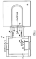
- the gas permeable plasma containing means is a perforated aluminum plate which extends transversely across the passageway.
- the plasma chamber preferably includes a second microwave oven, the cavity of which surrounds a second sample chamber extension, a second fluorine-containing gas supply into the second sample chamber extension, and second gas permeable plasma containing means in the second passageway. Efficient pretreatment of fluxless soldering samples is provided thereby.
- FIG. 1 schematically illustrates a side view of a preferred copper layer pre-treatment apparatus 10 used in accordance with the present invention.
- pre-treatment apparatus 10 includes a plasma energy generating chamber 12 , a sample treatment chamber 14 , and a passageway 16 connecting chambers 12 and 14 .
- the pre-treating exposing step is conducted to provide a fluorine/oxygen ratio on the copper surface of about 2/1 to about 8/1.
- a fluorine/oxygen ratio on the copper surface of about 2/1 to about 8/1.
- a second plasma energy generating chamber (not illustrated) is coupled to the sample chamber 14 opposite plasma energy chamber 12 , to provide a more thorough and equal distribution of the fluorine atoms onto the copper surface.
- the solder is reflowed to form either a solder bump or to reflow and join a second surface.
- the second surface may be a component or another solder bump.
- the copper surface can be dipped in a molten solder bath or wave and the copper surface "tinned" with the appropriate solder alloy.
- the process conditions for reflow can be selected to optimize reflow.
- reflow can be performed in an oxidizing atmosphere, i.e., air, or alternatively under an inert atmosphere, such as nitrogen.
- reflow can take place under atmospheric pressure or under vacuum pressure conditions, although the latter is not necessary.
- the plasma pre-treatment step and the reflow process may occur simultaneously and/or the second surface may be brought in contact with the solder during reflow.
- copper samples can be pre-treated in the sample pre-treatment chamber, removed and stored for up to one week under an oxidizing ambient, i.e., air, and then transported for successful joining in a different facility.
- pre-treated copper samples can be stored for up two weeks in an inert ambient, i.e., nitrogen, and then subjected to reflow conditions.
- the exposure of the copper layer can take place at room temperature (about 20 to 24°C).
- elevated temperatures can be used, i.e., the copper layer can be heated to a temperature up to about 120°C or higher.
- the plasma process is short in duration, i.e., about 15 to 30 minutes, and plasma pressures are from about 53 to 106 Pa (400 to 800 mTorr).
- the copper sample can optionally stored for up to one week under an oxidizing ambient, i.e., air.
- pre-treated copper samples can be stored for up two weeks in an inert ambient, i.e., nitrogen.
- solder is then placed on the copper surface as indicated in Block 50 .
- the solder is reflowed.
- Reflow can be performed in an oxidizing atmosphere, i.e., air, or alternatively under an inert atmosphere, such as nitrogen.
- reflow can take place under atmospheric pressure or under vacuum pressure conditions, although the latter is not necessary.
- reflow can take place at temperatures just above the melting point of the solder. For example, using a 63/37 weight percent tin/lead material, reflow takes place just above the melting point of the solder of 183°C at a temperature of about 200°C to 220°C.
- the reflow step can occur as part of a joining step.
- the testing was designed to determine the spreading index when the copper surfaces were pretreated in accordance with the present invention. Of interest were (a) spreading of an untreated solder disk on treated copper; (b) spreading of a treated solder disk on untreated copper; and (c) spreading of a treated solder disk on treated copper.
- Rapid reflow in air was also tested.
- a copper coupon with a solder disk on it was dropped on a hot stage maintained at 235°C to simulate a rapid reflow (dip) conditions.
- the heat-up time was on the order of a few seconds (less than five seconds).
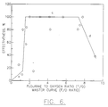
- FIG. 3 graphically illustrates the resultant wetting index of the samples. The scale is from 0 to 100. As seen from Figure 3, the best spreading index was obtained when both the copper and the solder disk were given the optimal treatment (S approximately 80%), which was better than when activated flux was used (S approximately 75%). The spreading of untreated solder on treated copper (S approximately 73%) was also close to the results obtained for activated flux. The spreading of solder on copper coupons in air with rapid reflow was about 69%. Temperature of pre-treatment had a marginal effect on spreading.
- Wavelength dispersive x-ray was used in this study on the bare copper printed circuit boards.
- WDX gives the concentrations of fluorine and oxygen on the surface of the samples. Once the ratio of the oxygen and fluorine contents were obtained, they were compared with the master curve generated using 1 mm eutectic solder disk samples.
- Printed circuit boards with bare copper were cleaned in alconox soap solution followed by a rinse in hot water and isopropyl alcohol. Pieces measuring 2,54 cm X 5,08 cm (1 inch x 2 inch) were cut from the board and pretreated at room temperature and at 120°C. A small piece was cut for surface analysis and the remaining piece was dipped in a pot of eutectic solder in air at 235°C. The piece was held there for 10 seconds and then pulled out.
Landscapes
- Engineering & Computer Science (AREA)
- Mechanical Engineering (AREA)
- Electric Connection Of Electric Components To Printed Circuits (AREA)
Claims (20)
- Verfahren zum Löten einer Kupferschicht (20) ohne Notwendigkeit von Flußmittel, folgende Schritte umfassend:Unterziehen einer Kupferschicht (20) mit einer Kupferoberfläche der Einwirkung eines fluorhaltigen Plasmas; undAufbringen von Lötmaterial auf die Kupferoberfläche der Kupferschicht.
- Verfahren nach Anspruch 1, wobei die Kupferoberfläche eine Oberflächlichenoxidschicht aufweist und wobei der Einwirkungsschritt zumindest ein Teil der Oberflächenoxide in fluorhaltige Verbindungen umwandelt.
- Verfahren nach Anspruch 2, wobei der Einwirkungsschritt ausgeführt wird, bis sich ausreichend fluorhaltige Verbindungen auf der Kupferoberfläche bilden, um das Benetzen mit Lötmaterial zu erlauben.
- Verfahren nach Anspruch 2, wobei der Einwirkungsschritt ein Fluor/Sauerstoff-Verhältnis auf der Kupferoberfläche von ungefähr 2/1 bis 8/1 zur Folge hat.
- Verfahren nach Anspruch 1, wobei der folgende Schritt zwischen dem Einwirkungsschritt und dem Aufbringungsschritt ausgeführt wird:Lagern der behandelten Kupferschicht (20) in einer Luftumgebung für eine Zeitdauer bis zu ungefähr einer Woche.
- Verfahren nach Anspruch 1, wobei der folgende Schritt zwischen dem Einwirkungsschritt und dem Aufbringungsschritt ausgeführt wird:Lagern der behandelten Kupferschicht (20) in einer inerten Umgebung für eine Zeitdauer bis ungefähr zwei Wochen.
- Verfahren nach Anspruch 1, das ferner einen Schritt umfaßt, bei dem das Lötmaterial auf der Oberfläche der Kupferschicht (20) nach dem Aufbringungsschritt verfließt.
- Verfahren nach Anspruch 7, wobei sich der Verfließschritt bei Atmosphärendruck vollzieht.
- Verfahren nach Anspruch 7, wobei sich der Verfließschritt in einer oxidierenden Umgebung vollzieht.
- Verfahren nach Anspruch 7, wobei sich der Verfließschritt in einer inerten Umgebung vollzieht.
- Verfahren nach Anspruch 7, wobei der Verfließschritt das Aufbringen des Lötmaterials in Berührung mit einer zweiten Oberfläche umfaßt, um so die Kupferoberfläche und die zweite Oberfläche miteinander zu verlöten, ohne eine nachträgliche Reinigung erforderlich zu machen.
- Verfahren nach Anspruch 1, wobei der Einwirkungsschritt folgende Schritte umfaßt:Unterziehen der Kupferschicht mit der Kupferoberfläche der Einwirkung eines fluorhaltigen Plasmas bei einem Druck von 53 bis 106 Pa (400 mTorr bis 800 mTorr) und bei einer Temperatur von 20°C bis 120°C für eine Zeitdauer von 15 bis 30 Minuten.
- Vorbehandlungssystem für Proben zum flußmittelfreien Löten, folgendes umfassend:eine Probenkammer (14) mit einer Öffnung;ein Probenhaltemittel (22) in der Probenkammer zum Halten der Probe;eine Probenkammererweiterung, die sich von der Öffnung der Probenkammer (14) nach außen erstreckt, um einen Durchgang (16) von der Probenkammererweiterung durch die Öffnung und in die Probenkammer (14) hinein zu definieren;Versorgungsmittel (18) für fluorhaltiges Gas zum Einleiten von fluorhaltigem Gas in die Probenkammererweiterung hinein;Energieerzeugungsmittel in der Probenkammererweiterung, um ein Plasma darin zu bilden und das fluorhaltige Gas in atomisches Fluor zu zerlegen; undein gasdurchlässiges, Plasma zurückhaltendes Mittel (19) in dem Durchgang, das den Durchtritt von Plasma durch den Durchgang (16) von der Probenkammererweiterung in die Probenkammer (14) hinein blockiert, während dem atomischen Fluor das Durchtreten durch den Durchgang (16) von der Probenkammererweiterung in die Probenkammer (14) hinein erlaubt ist, um so die Anregung der Probe mit fluorhaltigem Plasma durchzuführen.
- Vorbehandlungssystem nach Anspruch 13, wobei die Probenkammer (14) ferner eine zweite Öffnung beinhaltet, wobei das Vorbehandlungssystem weiter umfaßt:eine zweite Probenkammererweiterung, die sich von der zweiten Öffnung der Probenkammer nach außen erstreckt, um einen zweiten Durchgang von der zweiten Probenkammererweiterung durch die zweite Öffnung und in die Probenkammer hinein zu definieren;daß das Energieerzeugungsmittel ferner Energie in der zweiten Probenkammererweiterung erzeugt;daß das Versorgungsmittel für fluorhaltiges Gas ferner fluorhaltiges Gas in die zweite Probenkammererweiterung leitet; und daßein zweites gasdurchlässiges, Plasma zurückhaltendes Mittel in dem zweiten Durchgang vorgesehen ist, um das Durchtreten von Plasma durch den zweiten Durchgang von der zweiten Probenkammererweiterung zu der Probenkammer zu blockieren, während den Fluorradikalen das Durchtreten durch den zweiten Durchgang von der zweiten Probenkammererweiterung zu der Probenkammer erlaubt ist.
- Vorbehandlungssystem nach Anspruch 13, das ferner Mittel zum Erwärmen des Probenhaltemittels umfaßt, um so die Probe aufzuheizen.
- Vorbehandlungssystem nach Anspruch 13, wobei das Versorgungsmittel (18) für fluorhaltiges Gas eine Versorgungsleitung für fluorhaltiges Gas ist, die einen Auslaß in die Probenkammererweiterung aufweist.
- Vorbehandlungssystem nach Anspruch 16, wobei sich die Versorgungsleitung (18) für fluorhaltiges Gas von der Probenkammer (14) durch das gasdurchlässige Mittel (19), das das Plasma zurückhält, in die Probenkammererweiterung hinein erstreckt.
- Vorbehandlungssystem nach Anspruch 13, wobei das Energieerzeugungsmittel ein Mikrowellenenergieerzeugungsmittel umfaßt, um Mikrowellenenergie in der Probenkammererweiterung zu erzeugen.
- Vorbehandlungssystem nach Anspruch 18, wobei das Mikrowellenenergieerzeugungsmittel einen Mikrowellenofen umfaßt, der eine Mikrowellenofenhohlraum beinhaltet, wobei der Mikrowellenofenhohlraum die Probenkammererweiterung umgibt.
- Vorbehandlungssystem nach Anspruch 13, wobei das gasdurchlässige Mittel, das das Plasma zurückhält, eine perforierte Aluminiumplatte (19) umfaßt, die sich quer durch den Durchgang (16) erstreckt, um das Durchtreten des Plasma durch den Durchgang (16) von der Probenkammererweiterung in die Probenkammer (14) hinein zu blockieren, während dem atomischen Fluor das Durchtreten durch den Durchgang (16) von der Probenkammererweiterung in die Probenkammer (14) erlaubt ist, um so die Anregung der Probe mit fluorhaltigem Plasma durchzuführen.
Applications Claiming Priority (5)
| Application Number | Priority Date | Filing Date | Title |
|---|---|---|---|
| US155020 | 1993-11-19 | ||
| US08/155,020 US5407121A (en) | 1993-11-19 | 1993-11-19 | Fluxless soldering of copper |
| US08/339,770 US5499754A (en) | 1993-11-19 | 1994-11-15 | Fluxless soldering sample pretreating system |
| US339770 | 1994-11-15 | ||
| PCT/US1994/013371 WO1995013896A1 (en) | 1993-11-19 | 1994-11-16 | Fluxless soldering pretreating system and method using fluorine-containing plasma |
Publications (3)
| Publication Number | Publication Date |
|---|---|
| EP0729397A1 EP0729397A1 (de) | 1996-09-04 |
| EP0729397B1 true EP0729397B1 (de) | 1998-06-10 |
| EP0729397B2 EP0729397B2 (de) | 2001-09-19 |
Family
ID=26851941
Family Applications (1)
| Application Number | Title | Priority Date | Filing Date |
|---|---|---|---|
| EP95902622A Expired - Lifetime EP0729397B2 (de) | 1993-11-19 | 1994-11-16 | Vorbehandlungssystem zum flussmittelfreien löten und verfahren unter verwendung eines fluorhaltigen plasmas |
Country Status (7)
| Country | Link |
|---|---|
| US (1) | US5499754A (de) |
| EP (1) | EP0729397B2 (de) |
| JP (1) | JP3153815B2 (de) |
| AT (1) | ATE167097T1 (de) |
| AU (1) | AU1182595A (de) |
| DE (1) | DE69411031D1 (de) |
| WO (1) | WO1995013896A1 (de) |
Families Citing this family (37)
| Publication number | Priority date | Publication date | Assignee | Title |
|---|---|---|---|---|
| WO1994022628A1 (fr) * | 1993-04-05 | 1994-10-13 | Seiko Epson Corporation | Procede et appareil d'assemblage par brasage |
| JP3312377B2 (ja) * | 1993-12-09 | 2002-08-05 | セイコーエプソン株式会社 | ろう材による接合方法及び装置 |
| US6342275B1 (en) | 1993-12-24 | 2002-01-29 | Seiko Epson Corporation | Method and apparatus for atmospheric pressure plasma surface treatment, method of manufacturing semiconductor device, and method of manufacturing ink jet printing head |
| US6006763A (en) * | 1995-01-11 | 1999-12-28 | Seiko Epson Corporation | Surface treatment method |
| JP3521587B2 (ja) * | 1995-02-07 | 2004-04-19 | セイコーエプソン株式会社 | 基板周縁の不要物除去方法及び装置並びにそれを用いた塗布方法 |
| JPH08279495A (ja) * | 1995-02-07 | 1996-10-22 | Seiko Epson Corp | プラズマ処理装置及びその方法 |
| WO1996031997A1 (en) * | 1995-04-07 | 1996-10-10 | Seiko Epson Corporation | Surface treatment apparatus |
| JP3598602B2 (ja) * | 1995-08-07 | 2004-12-08 | セイコーエプソン株式会社 | プラズマエッチング方法、液晶表示パネルの製造方法、及びプラズマエッチング装置 |
| JPH09233862A (ja) * | 1995-12-18 | 1997-09-05 | Seiko Epson Corp | 圧電体を用いた発電方法、発電装置および電子機器 |
| JPH09312545A (ja) | 1996-03-18 | 1997-12-02 | Seiko Epson Corp | 圧電素子、その製造方法、及び圧電振動片のマウント装置 |
| US5918354A (en) * | 1996-04-02 | 1999-07-06 | Seiko Epson Corporation | Method of making a piezoelectric element |
| US5866986A (en) * | 1996-08-05 | 1999-02-02 | Integrated Electronic Innovations, Inc. | Microwave gas phase plasma source |
| US5992729A (en) * | 1996-10-02 | 1999-11-30 | Mcnc | Tacking processes and systems for soldering |
| DE19643865C2 (de) * | 1996-10-30 | 1999-04-08 | Schott Glas | Plasmaunterstütztes chemisches Abscheidungsverfahren (CVD) mit entfernter Anregung eines Anregungsgases (Remote-Plasma-CVD-Verfahren) zur Beschichtung oder zur Behandlung großflächiger Substrate und Vorrichtung zur Durchführung desselben |
| US5902686A (en) * | 1996-11-21 | 1999-05-11 | Mcnc | Methods for forming an intermetallic region between a solder bump and an under bump metallurgy layer and related structures |
| US5776551A (en) * | 1996-12-23 | 1998-07-07 | Lsi Logic Corporation | Use of plasma activated NF3 to clean solder bumps on a device |
| US6142358A (en) * | 1997-05-31 | 2000-11-07 | The Regents Of The University Of California | Wafer-to-wafer transfer of microstructures using break-away tethers |
| JP4497154B2 (ja) * | 1997-12-15 | 2010-07-07 | セイコーエプソン株式会社 | 固体接合方法 |
| US6607613B2 (en) | 1998-07-10 | 2003-08-19 | International Business Machines Corporation | Solder ball with chemically and mechanically enhanced surface properties |
| US6250540B1 (en) * | 1999-04-30 | 2001-06-26 | International Business Machines Corporation | Fluxless joining process for enriched solders |
| US6056831A (en) | 1998-07-10 | 2000-05-02 | International Business Machines Corporation | Process for chemically and mechanically enhancing solder surface properties |
| US6742701B2 (en) * | 1998-09-17 | 2004-06-01 | Kabushiki Kaisha Tamura Seisakusho | Bump forming method, presoldering treatment method, soldering method, bump forming apparatus, presoldering treatment device and soldering apparatus |
| US6206276B1 (en) | 1999-09-13 | 2001-03-27 | Lucent Technologies Inc. | Direct-placement fluxless soldering using inert gas environment |
| US6193135B1 (en) | 1999-09-13 | 2001-02-27 | Lucent Technologies Inc. | System for providing back-lighting of components during fluxless soldering |
| US6196446B1 (en) | 1999-09-13 | 2001-03-06 | Lucent Technologies Inc. | Automated fluxless soldering using inert gas |
| JP2002231724A (ja) * | 2001-01-30 | 2002-08-16 | Nec Corp | 配線の形成方法 |
| DE10210216A1 (de) * | 2002-03-08 | 2003-10-16 | Behr Gmbh & Co | Verfahren zum Löten von Aluminium |
| US6936546B2 (en) * | 2002-04-26 | 2005-08-30 | Accretech Usa, Inc. | Apparatus for shaping thin films in the near-edge regions of in-process semiconductor substrates |
| US20080011332A1 (en) * | 2002-04-26 | 2008-01-17 | Accretech Usa, Inc. | Method and apparatus for cleaning a wafer substrate |
| US20080190558A1 (en) * | 2002-04-26 | 2008-08-14 | Accretech Usa, Inc. | Wafer processing apparatus and method |
| US20080017316A1 (en) * | 2002-04-26 | 2008-01-24 | Accretech Usa, Inc. | Clean ignition system for wafer substrate processing |
| US6949398B2 (en) * | 2002-10-31 | 2005-09-27 | Freescale Semiconductor, Inc. | Low cost fabrication and assembly of lid for semiconductor devices |
| US7332424B2 (en) * | 2004-08-16 | 2008-02-19 | International Business Machines Corporation | Fluxless solder transfer and reflow process |
| CN104425289B (zh) * | 2013-09-11 | 2017-12-15 | 先进科技新加坡有限公司 | 利用激发的混合气体的晶粒安装装置和方法 |
| CN105252099B (zh) * | 2015-11-24 | 2017-07-11 | 武汉工程大学 | 一种利用微波等离子体焊接金刚石真空窗口的方法 |
| US10879211B2 (en) * | 2016-06-30 | 2020-12-29 | R.S.M. Electron Power, Inc. | Method of joining a surface-mount component to a substrate with solder that has been temporarily secured |
| US11217550B2 (en) * | 2018-07-24 | 2022-01-04 | Xilinx, Inc. | Chip package assembly with enhanced interconnects and method for fabricating the same |
Family Cites Families (28)
| Publication number | Priority date | Publication date | Assignee | Title |
|---|---|---|---|---|
| FR2294014A1 (fr) * | 1974-12-13 | 1976-07-09 | Cerca | Procede d'assemblage a chaud |
| US4012307A (en) * | 1975-12-05 | 1977-03-15 | General Dynamics Corporation | Method for conditioning drilled holes in multilayer wiring boards |
| US4188237A (en) * | 1978-02-02 | 1980-02-12 | University Of Dayton | Method for cleaning metal parts with elemental fluorine |
| US4328044A (en) * | 1978-02-02 | 1982-05-04 | University Of Dayton | Method for cleaning metal parts |
| US4405379A (en) * | 1980-02-06 | 1983-09-20 | University Of Dayton | Method for cleaning metal parts |
| DE3206809A1 (de) * | 1982-02-25 | 1983-02-17 | Hans-Friedrich Dipl.-Ing. 8000 München Tölke | Verfahren zum loeten von schnelloxidierenden metallen, insbesondere von aluminium, im vakuum oder unter schutzgas nach vorheriger beseitigung der oxidschicht durch amalgamierung |
| US4504007A (en) * | 1982-09-14 | 1985-03-12 | International Business Machines Corporation | Solder and braze fluxes and processes for using the same |
| US4498046A (en) * | 1982-10-18 | 1985-02-05 | International Business Machines Corporation | Room temperature cryogenic test interface |
| CH662007A5 (en) * | 1983-12-21 | 1987-08-31 | Bbc Brown Boveri & Cie | Method of soldering semiconductor components |
| US4577398A (en) * | 1984-09-07 | 1986-03-25 | Trilogy Computer Development Partners, Ltd. | Method for mounting a semiconductor chip |
| JPS6269620A (ja) * | 1985-09-24 | 1987-03-30 | Anelva Corp | プラズマ処理装置 |
| US4646958A (en) * | 1985-10-31 | 1987-03-03 | International Business Machines Corp. | Fluxless soldering process using a silane atmosphere |
| US4821947A (en) * | 1988-02-08 | 1989-04-18 | Union Carbide Corporation | Fluxless application of a metal-comprising coating |
| US5071058A (en) * | 1988-09-30 | 1991-12-10 | Union Carbide Industrial Gases Technology Corporation | Process for joining/coating using an atmosphere having a controlled oxidation capability |
| GB8827933D0 (en) * | 1988-11-30 | 1989-01-05 | Plessey Co Plc | Improvements relating to soldering processes |
| JP2625997B2 (ja) * | 1988-12-02 | 1997-07-02 | 富士通株式会社 | フラックスレス接合方法 |
| US4921157A (en) * | 1989-03-15 | 1990-05-01 | Microelectronics Center Of North Carolina | Fluxless soldering process |
| DE4032328A1 (de) * | 1989-11-06 | 1991-09-19 | Wls Karl Heinz Grasmann Weichl | Verfahren und vorrichtung zur verarbeitung von zu verloetenden fuegepartnern |
| US4979664A (en) * | 1989-11-15 | 1990-12-25 | At&T Bell Laboratories | Method for manufacturing a soldered article |
| US5121874A (en) * | 1989-11-22 | 1992-06-16 | Electrovert Ltd. | Shield gas wave soldering |
| US5048746A (en) * | 1989-12-08 | 1991-09-17 | Electrovert Ltd. | Tunnel for fluxless soldering |
| US5090651A (en) * | 1990-01-31 | 1992-02-25 | Electrovert Ltd. | Gas curtain additives and zoned tunnel for soldering |
| US5139193A (en) * | 1990-06-04 | 1992-08-18 | Toddco General, Inc. | Fluxless resoldering system and fluxless soldering process |
| US5164566A (en) * | 1990-06-12 | 1992-11-17 | Microelectronics And Computer Technology Corp. | Method and apparatus for fluxless solder reflow |
| DE4041270A1 (de) * | 1990-12-21 | 1992-06-25 | Grasmann Karl Heinz Wls | Verfahren und vorrichtung zur verarbeitung von elektronischen flachbaugruppen, insbesondere mit bauelementen bestueckten leiterplatten |
| US5145104A (en) * | 1991-03-21 | 1992-09-08 | International Business Machines Corporation | Substrate soldering in a reducing atmosphere |
| US5158224A (en) * | 1992-02-24 | 1992-10-27 | Robotic Process Systems, Inc. | Soldering machine having a vertical transfer oven |
| DE4225378A1 (de) | 1992-03-20 | 1993-09-23 | Linde Ag | Verfahren zum verloeten von leiterplatten unter niederdruck |
-
1994
- 1994-11-15 US US08/339,770 patent/US5499754A/en not_active Expired - Fee Related
- 1994-11-16 WO PCT/US1994/013371 patent/WO1995013896A1/en not_active Ceased
- 1994-11-16 EP EP95902622A patent/EP0729397B2/de not_active Expired - Lifetime
- 1994-11-16 AU AU11825/95A patent/AU1182595A/en not_active Abandoned
- 1994-11-16 AT AT95902622T patent/ATE167097T1/de active
- 1994-11-16 JP JP51463895A patent/JP3153815B2/ja not_active Expired - Fee Related
- 1994-11-16 DE DE69411031T patent/DE69411031D1/de not_active Expired - Lifetime
Also Published As
| Publication number | Publication date |
|---|---|
| AU1182595A (en) | 1995-06-06 |
| EP0729397B2 (de) | 2001-09-19 |
| JPH09505001A (ja) | 1997-05-20 |
| JP3153815B2 (ja) | 2001-04-09 |
| WO1995013896A1 (en) | 1995-05-26 |
| DE69411031D1 (de) | 1998-07-16 |
| EP0729397A1 (de) | 1996-09-04 |
| US5499754A (en) | 1996-03-19 |
| ATE167097T1 (de) | 1998-06-15 |
Similar Documents
| Publication | Publication Date | Title |
|---|---|---|
| EP0729397B1 (de) | Vorbehandlungssystem zum flussmittelfreien löten und verfahren unter verwendung eines fluorhaltigen plasmas | |
| US5407121A (en) | Fluxless soldering of copper | |
| US4921157A (en) | Fluxless soldering process | |
| EP0879112B1 (de) | Flussmittelfreiverfahren | |
| US5145104A (en) | Substrate soldering in a reducing atmosphere | |
| US5164566A (en) | Method and apparatus for fluxless solder reflow | |
| US5878943A (en) | Method of fabricating an electronic circuit device and apparatus for performing the method | |
| US6935553B2 (en) | Reflow soldering method | |
| US20060183270A1 (en) | Tools and methods for forming conductive bumps on microelectronic elements | |
| JP4252631B2 (ja) | はんだ接合用表面の清浄方法及び改質方法並びにはんだ付け方法 | |
| Koopman et al. | Fluxless soldering in air and nitrogen | |
| EP0410623B1 (de) | Verfahren und Vorrichtung zum Löten von Gegenständen | |
| Kralova et al. | Wettability in lead-free soldering: Effect of plasma treatment in dependence on flux type | |
| US6092714A (en) | Method of utilizing a plasma gas mixture containing argon and CF4 to clean and coat a conductor | |
| JP2000042786A (ja) | はんだ付け用水溶性フラックス | |
| Liu et al. | Fluxless soldering of copper substrates using self-assembled monolayers for preservation | |
| US7159758B1 (en) | Circuit board processing techniques using solder fusing | |
| JPH09307219A (ja) | はんだ付け用処理方法 | |
| KR100292295B1 (ko) | 레이저를 이용한 웨이퍼 레벨의 무플럭스 솔더 접합 장치 및 방법 | |
| KR940001030B1 (ko) | 조절된 산화능력을 갖는 대기를 사용하는 결합/피복방법 | |
| Sorokina et al. | Influence of No-Clean Flux on the Corrosivity of Various Surface Finishes After Reflow | |
| Hillman | Reduced Oxide Soldering Activation (ROSA): Enabling Technology for Soldering of Flip Chip Assemblies | |
| Hosking et al. | Fluxless laser soldering for electronic packaging | |
| Jellison et al. | Advanced soldering processes | |
| Hernandez et al. | Effects of pre-stressing and flux on the flow of solder on PWB copper surfaces |
Legal Events
| Date | Code | Title | Description |
|---|---|---|---|
| PUAI | Public reference made under article 153(3) epc to a published international application that has entered the european phase |
Free format text: ORIGINAL CODE: 0009012 |
|
| 17P | Request for examination filed |
Effective date: 19960615 |
|
| AK | Designated contracting states |
Kind code of ref document: A1 Designated state(s): AT BE CH DE DK ES FR GB GR IE IT LI LU MC NL PT SE |
|
| GRAG | Despatch of communication of intention to grant |
Free format text: ORIGINAL CODE: EPIDOS AGRA |
|
| 17Q | First examination report despatched |
Effective date: 19970806 |
|
| GRAG | Despatch of communication of intention to grant |
Free format text: ORIGINAL CODE: EPIDOS AGRA |
|
| GRAG | Despatch of communication of intention to grant |
Free format text: ORIGINAL CODE: EPIDOS AGRA |
|
| GRAH | Despatch of communication of intention to grant a patent |
Free format text: ORIGINAL CODE: EPIDOS IGRA |
|
| GRAH | Despatch of communication of intention to grant a patent |
Free format text: ORIGINAL CODE: EPIDOS IGRA |
|
| GRAA | (expected) grant |
Free format text: ORIGINAL CODE: 0009210 |
|
| AK | Designated contracting states |
Kind code of ref document: B1 Designated state(s): AT BE CH DE DK ES FR GB GR IE IT LI LU MC NL PT SE |
|
| PG25 | Lapsed in a contracting state [announced via postgrant information from national office to epo] |
Ref country code: NL Free format text: LAPSE BECAUSE OF FAILURE TO SUBMIT A TRANSLATION OF THE DESCRIPTION OR TO PAY THE FEE WITHIN THE PRESCRIBED TIME-LIMIT Effective date: 19980610 Ref country code: LI Free format text: LAPSE BECAUSE OF FAILURE TO SUBMIT A TRANSLATION OF THE DESCRIPTION OR TO PAY THE FEE WITHIN THE PRESCRIBED TIME-LIMIT Effective date: 19980610 Ref country code: IT Free format text: LAPSE BECAUSE OF FAILURE TO SUBMIT A TRANSLATION OF THE DESCRIPTION OR TO PAY THE FEE WITHIN THE PRE;WARNING: LAPSES OF ITALIAN PATENTS WITH EFFECTIVE DATE BEFORE 2007 MAY HAVE OCCURRED AT ANY TIME BEFORE 2007. THE CORRECT EFFECTIVE DATE MAY BE DIFFERENT FROM THE ONE RECORDED.SCRIBED TIME-LIMIT Effective date: 19980610 Ref country code: GR Free format text: LAPSE BECAUSE OF NON-PAYMENT OF DUE FEES Effective date: 19980610 Ref country code: FR Free format text: LAPSE BECAUSE OF FAILURE TO SUBMIT A TRANSLATION OF THE DESCRIPTION OR TO PAY THE FEE WITHIN THE PRESCRIBED TIME-LIMIT Effective date: 19980610 Ref country code: ES Free format text: THE PATENT HAS BEEN ANNULLED BY A DECISION OF A NATIONAL AUTHORITY Effective date: 19980610 Ref country code: CH Free format text: LAPSE BECAUSE OF FAILURE TO SUBMIT A TRANSLATION OF THE DESCRIPTION OR TO PAY THE FEE WITHIN THE PRESCRIBED TIME-LIMIT Effective date: 19980610 Ref country code: BE Free format text: LAPSE BECAUSE OF FAILURE TO SUBMIT A TRANSLATION OF THE DESCRIPTION OR TO PAY THE FEE WITHIN THE PRESCRIBED TIME-LIMIT Effective date: 19980610 Ref country code: AT Free format text: LAPSE BECAUSE OF FAILURE TO SUBMIT A TRANSLATION OF THE DESCRIPTION OR TO PAY THE FEE WITHIN THE PRESCRIBED TIME-LIMIT Effective date: 19980610 |
|
| REF | Corresponds to: |
Ref document number: 167097 Country of ref document: AT Date of ref document: 19980615 Kind code of ref document: T |
|
| REG | Reference to a national code |
Ref country code: CH Ref legal event code: EP |
|
| REF | Corresponds to: |
Ref document number: 69411031 Country of ref document: DE Date of ref document: 19980716 |
|
| PG25 | Lapsed in a contracting state [announced via postgrant information from national office to epo] |
Ref country code: SE Free format text: LAPSE BECAUSE OF FAILURE TO SUBMIT A TRANSLATION OF THE DESCRIPTION OR TO PAY THE FEE WITHIN THE PRESCRIBED TIME-LIMIT Effective date: 19980910 Ref country code: DK Free format text: LAPSE BECAUSE OF FAILURE TO SUBMIT A TRANSLATION OF THE DESCRIPTION OR TO PAY THE FEE WITHIN THE PRESCRIBED TIME-LIMIT Effective date: 19980910 |
|
| PG25 | Lapsed in a contracting state [announced via postgrant information from national office to epo] |
Ref country code: DE Free format text: LAPSE BECAUSE OF FAILURE TO SUBMIT A TRANSLATION OF THE DESCRIPTION OR TO PAY THE FEE WITHIN THE PRESCRIBED TIME-LIMIT Effective date: 19980911 |
|
| PG25 | Lapsed in a contracting state [announced via postgrant information from national office to epo] |
Ref country code: PT Free format text: LAPSE BECAUSE OF FAILURE TO SUBMIT A TRANSLATION OF THE DESCRIPTION OR TO PAY THE FEE WITHIN THE PRESCRIBED TIME-LIMIT Effective date: 19980915 |
|
| REG | Reference to a national code |
Ref country code: IE Ref legal event code: FG4D |
|
| NLV1 | Nl: lapsed or annulled due to failure to fulfill the requirements of art. 29p and 29m of the patents act | ||
| EN | Fr: translation not filed | ||
| PG25 | Lapsed in a contracting state [announced via postgrant information from national office to epo] |
Ref country code: LU Free format text: LAPSE BECAUSE OF NON-PAYMENT OF DUE FEES Effective date: 19981116 Ref country code: IE Free format text: LAPSE BECAUSE OF NON-PAYMENT OF DUE FEES Effective date: 19981116 |
|
| REG | Reference to a national code |
Ref country code: CH Ref legal event code: PL |
|
| PLBQ | Unpublished change to opponent data |
Free format text: ORIGINAL CODE: EPIDOS OPPO |
|
| PLBI | Opposition filed |
Free format text: ORIGINAL CODE: 0009260 |
|
| PLBQ | Unpublished change to opponent data |
Free format text: ORIGINAL CODE: EPIDOS OPPO |
|
| PLAB | Opposition data, opponent's data or that of the opponent's representative modified |
Free format text: ORIGINAL CODE: 0009299OPPO |
|
| PLBF | Reply of patent proprietor to notice(s) of opposition |
Free format text: ORIGINAL CODE: EPIDOS OBSO |
|
| 26 | Opposition filed |
Opponent name: LINDE AKTIENGESELLSCHAFT Effective date: 19990310 |
|
| R26 | Opposition filed (corrected) |
Opponent name: LINDE AKTIENGESELLSCHAFT, WIESBADEN Effective date: 19990310 |
|
| PG25 | Lapsed in a contracting state [announced via postgrant information from national office to epo] |
Ref country code: MC Free format text: LAPSE BECAUSE OF NON-PAYMENT OF DUE FEES Effective date: 19990531 |
|
| PLBF | Reply of patent proprietor to notice(s) of opposition |
Free format text: ORIGINAL CODE: EPIDOS OBSO |
|
| REG | Reference to a national code |
Ref country code: IE Ref legal event code: MM4A |
|
| PLBF | Reply of patent proprietor to notice(s) of opposition |
Free format text: ORIGINAL CODE: EPIDOS OBSO |
|
| PGFP | Annual fee paid to national office [announced via postgrant information from national office to epo] |
Ref country code: GB Payment date: 20001115 Year of fee payment: 7 |
|
| PLAW | Interlocutory decision in opposition |
Free format text: ORIGINAL CODE: EPIDOS IDOP |
|
| PLAW | Interlocutory decision in opposition |
Free format text: ORIGINAL CODE: EPIDOS IDOP |
|
| PUAH | Patent maintained in amended form |
Free format text: ORIGINAL CODE: 0009272 |
|
| STAA | Information on the status of an ep patent application or granted ep patent |
Free format text: STATUS: PATENT MAINTAINED AS AMENDED |
|
| 27A | Patent maintained in amended form |
Effective date: 20010919 |
|
| AK | Designated contracting states |
Kind code of ref document: B2 Designated state(s): AT BE CH DE DK ES FR GB GR IE IT LI LU MC NL PT SE |
|
| PG25 | Lapsed in a contracting state [announced via postgrant information from national office to epo] |
Ref country code: GB Free format text: LAPSE BECAUSE OF NON-PAYMENT OF DUE FEES Effective date: 20011116 |
|
| REG | Reference to a national code |
Ref country code: GB Ref legal event code: IF02 |
|
| EN | Fr: translation not filed |