EP0728369B1 - Materiau multicouches et dispositif comprenant ce materiau - Google Patents
Materiau multicouches et dispositif comprenant ce materiau Download PDFInfo
- Publication number
- EP0728369B1 EP0728369B1 EP95901480A EP95901480A EP0728369B1 EP 0728369 B1 EP0728369 B1 EP 0728369B1 EP 95901480 A EP95901480 A EP 95901480A EP 95901480 A EP95901480 A EP 95901480A EP 0728369 B1 EP0728369 B1 EP 0728369B1
- Authority
- EP
- European Patent Office
- Prior art keywords
- layers
- material according
- oxide
- superconducting
- superconductive
- Prior art date
- Legal status (The legal status is an assumption and is not a legal conclusion. Google has not performed a legal analysis and makes no representation as to the accuracy of the status listed.)
- Expired - Lifetime
Links
- 239000000463 material Substances 0.000 title claims abstract description 39
- 239000000758 substrate Substances 0.000 claims abstract description 18
- QPLDLSVMHZLSFG-UHFFFAOYSA-N Copper oxide Chemical compound [Cu]=O QPLDLSVMHZLSFG-UHFFFAOYSA-N 0.000 claims abstract description 9
- 239000005751 Copper oxide Substances 0.000 claims abstract description 6
- 229910000431 copper oxide Inorganic materials 0.000 claims abstract description 6
- 239000000126 substance Substances 0.000 claims abstract description 5
- 229910052712 strontium Inorganic materials 0.000 claims abstract description 4
- CIOAGBVUUVVLOB-UHFFFAOYSA-N strontium atom Chemical compound [Sr] CIOAGBVUUVVLOB-UHFFFAOYSA-N 0.000 claims abstract description 4
- -1 Ca2+ ion Chemical class 0.000 claims abstract 2
- 239000011575 calcium Substances 0.000 claims description 14
- 229910044991 metal oxide Inorganic materials 0.000 claims description 10
- 150000004706 metal oxides Chemical class 0.000 claims description 10
- 239000010949 copper Substances 0.000 claims description 7
- ODINCKMPIJJUCX-UHFFFAOYSA-N calcium oxide Inorganic materials [Ca]=O ODINCKMPIJJUCX-UHFFFAOYSA-N 0.000 claims description 5
- 229910052802 copper Inorganic materials 0.000 claims description 5
- BRPQOXSCLDDYGP-UHFFFAOYSA-N calcium oxide Chemical compound [O-2].[Ca+2] BRPQOXSCLDDYGP-UHFFFAOYSA-N 0.000 claims description 4
- 239000000292 calcium oxide Substances 0.000 claims description 4
- 229910052751 metal Inorganic materials 0.000 claims description 4
- 239000002184 metal Substances 0.000 claims description 4
- 229910000416 bismuth oxide Inorganic materials 0.000 claims description 3
- TYIXMATWDRGMPF-UHFFFAOYSA-N dibismuth;oxygen(2-) Chemical compound [O-2].[O-2].[O-2].[Bi+3].[Bi+3] TYIXMATWDRGMPF-UHFFFAOYSA-N 0.000 claims description 3
- 229910052716 thallium Inorganic materials 0.000 claims description 3
- 239000010410 layer Substances 0.000 description 57
- JCXGWMGPZLAOME-UHFFFAOYSA-N bismuth atom Chemical compound [Bi] JCXGWMGPZLAOME-UHFFFAOYSA-N 0.000 description 9
- OYPRJOBELJOOCE-UHFFFAOYSA-N Calcium Chemical compound [Ca] OYPRJOBELJOOCE-UHFFFAOYSA-N 0.000 description 8
- QVGXLLKOCUKJST-UHFFFAOYSA-N atomic oxygen Chemical compound [O] QVGXLLKOCUKJST-UHFFFAOYSA-N 0.000 description 8
- 229910052797 bismuth Inorganic materials 0.000 description 8
- 229910052791 calcium Inorganic materials 0.000 description 8
- 238000010438 heat treatment Methods 0.000 description 8
- 238000000034 method Methods 0.000 description 6
- 238000004519 manufacturing process Methods 0.000 description 5
- RYGMFSIKBFXOCR-UHFFFAOYSA-N Copper Chemical compound [Cu] RYGMFSIKBFXOCR-UHFFFAOYSA-N 0.000 description 4
- 230000015572 biosynthetic process Effects 0.000 description 4
- MYMOFIZGZYHOMD-UHFFFAOYSA-N Dioxygen Chemical compound O=O MYMOFIZGZYHOMD-UHFFFAOYSA-N 0.000 description 3
- 238000000151 deposition Methods 0.000 description 3
- 229910001882 dioxygen Inorganic materials 0.000 description 3
- 229910052760 oxygen Inorganic materials 0.000 description 3
- 239000001301 oxygen Substances 0.000 description 3
- 238000002128 reflection high energy electron diffraction Methods 0.000 description 3
- 230000008021 deposition Effects 0.000 description 2
- 230000004907 flux Effects 0.000 description 2
- 150000002500 ions Chemical class 0.000 description 2
- 239000000395 magnesium oxide Substances 0.000 description 2
- CPLXHLVBOLITMK-UHFFFAOYSA-N magnesium oxide Inorganic materials [Mg]=O CPLXHLVBOLITMK-UHFFFAOYSA-N 0.000 description 2
- AXZKOIWUVFPNLO-UHFFFAOYSA-N magnesium;oxygen(2-) Chemical compound [O-2].[Mg+2] AXZKOIWUVFPNLO-UHFFFAOYSA-N 0.000 description 2
- RZVAJINKPMORJF-UHFFFAOYSA-N Acetaminophen Chemical compound CC(=O)NC1=CC=C(O)C=C1 RZVAJINKPMORJF-UHFFFAOYSA-N 0.000 description 1
- 241000238366 Cephalopoda Species 0.000 description 1
- 240000008042 Zea mays Species 0.000 description 1
- 238000002679 ablation Methods 0.000 description 1
- 238000000429 assembly Methods 0.000 description 1
- 230000000712 assembly Effects 0.000 description 1
- 239000013078 crystal Substances 0.000 description 1
- 238000009792 diffusion process Methods 0.000 description 1
- 230000000694 effects Effects 0.000 description 1
- 238000010894 electron beam technology Methods 0.000 description 1
- 238000002003 electron diffraction Methods 0.000 description 1
- 238000000407 epitaxy Methods 0.000 description 1
- 230000008020 evaporation Effects 0.000 description 1
- 238000001704 evaporation Methods 0.000 description 1
- 239000011229 interlayer Substances 0.000 description 1
- 238000000608 laser ablation Methods 0.000 description 1
- QSHDDOUJBYECFT-UHFFFAOYSA-N mercury Chemical compound [Hg] QSHDDOUJBYECFT-UHFFFAOYSA-N 0.000 description 1
- 229910052753 mercury Inorganic materials 0.000 description 1
- 238000012544 monitoring process Methods 0.000 description 1
- 230000001590 oxidative effect Effects 0.000 description 1
- 230000035515 penetration Effects 0.000 description 1
- 239000000523 sample Substances 0.000 description 1
- 241000894007 species Species 0.000 description 1
- VEALVRVVWBQVSL-UHFFFAOYSA-N strontium titanate Chemical compound [Sr+2].[O-][Ti]([O-])=O VEALVRVVWBQVSL-UHFFFAOYSA-N 0.000 description 1
- 239000002887 superconductor Substances 0.000 description 1
Images
Classifications
-
- H—ELECTRICITY
- H10—SEMICONDUCTOR DEVICES; ELECTRIC SOLID-STATE DEVICES NOT OTHERWISE PROVIDED FOR
- H10N—ELECTRIC SOLID-STATE DEVICES NOT OTHERWISE PROVIDED FOR
- H10N60/00—Superconducting devices
- H10N60/80—Constructional details
- H10N60/85—Superconducting active materials
- H10N60/855—Ceramic superconductors
- H10N60/857—Ceramic superconductors comprising copper oxide
-
- H—ELECTRICITY
- H10—SEMICONDUCTOR DEVICES; ELECTRIC SOLID-STATE DEVICES NOT OTHERWISE PROVIDED FOR
- H10N—ELECTRIC SOLID-STATE DEVICES NOT OTHERWISE PROVIDED FOR
- H10N60/00—Superconducting devices
- H10N60/01—Manufacture or treatment
-
- Y—GENERAL TAGGING OF NEW TECHNOLOGICAL DEVELOPMENTS; GENERAL TAGGING OF CROSS-SECTIONAL TECHNOLOGIES SPANNING OVER SEVERAL SECTIONS OF THE IPC; TECHNICAL SUBJECTS COVERED BY FORMER USPC CROSS-REFERENCE ART COLLECTIONS [XRACs] AND DIGESTS
- Y10—TECHNICAL SUBJECTS COVERED BY FORMER USPC
- Y10S—TECHNICAL SUBJECTS COVERED BY FORMER USPC CROSS-REFERENCE ART COLLECTIONS [XRACs] AND DIGESTS
- Y10S428/00—Stock material or miscellaneous articles
- Y10S428/922—Static electricity metal bleed-off metallic stock
- Y10S428/9265—Special properties
- Y10S428/93—Electric superconducting
Definitions
- the present invention relates to a superconductive material in the form of a film consisting of monomolecular layers which are superimposed on each other on a substrate, comprising at least a first set of layers which constitutes a reservoir of electrical charges, and at minus a second set of layers that forms a cell superconductive and which is made up of a number n of superconductive layers separated from each other by intermediate layers, the charge tank and the superconducting cell being contiguous in the stack of layers.
- the term "monomolecular layer” means a layer consisting of a thickness single atom or molecule constituting said layer.
- a material as defined above is disclosed for example in document EP-A-0 305 292.
- the superconductive layers consist of a planar copper oxide, in general CuO 2 , often called cuprate.
- Known superconductive materials have a critical temperature not exceeding 135 K at pressure atmospheric, and 155 K under very high pressure.
- the object of the present invention is to remedy this disadvantage.
- a superconductive material of the kind in question is essentially characterized in that the intermediate layers have the chemical formula Ca 1-x M x and are free of strontium, x being a real number greater than 0 and at most equal to 0.2, M being a substituted element having an ionic radius close to that of the Ca 2+ ion, the intermediate layers being complete or having gaps.
- the critical temperature of the superconducting material is very markedly increased and reaches, in at least one example, 250 K.
- the growth mechanism of the layers is strictly monomolecular (atomic layer after atomic layer) for avoid mixing by thermal diffusion of the layers already filed.
- the present invention also relates to components comprising a material as defined above, in particular components using the resistance close to zero of the superconductive material, such as interconnects, fast transistors and microwave components, or components using junctions Josephson, such as superconducting devices quantum interference (“SQUID”), and the switching or fast memory for electronics digital.
- components comprising a material as defined above, in particular components using the resistance close to zero of the superconductive material, such as interconnects, fast transistors and microwave components, or components using junctions Josephson, such as superconducting devices quantum interference (“SQUID”), and the switching or fast memory for electronics digital.
- SQUID superconducting devices quantum interference
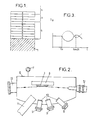
- the superconductive material according to the invention is in the form of a multilayer film deposited on a perfectly polished substrate 1, preferably a single crystal of strontium titanate (SrTiO 3 ) or magnesium oxide (MgO), or the like.
- the film which is deposited on the substrate 1 is consisting of superimposed monomolecular layers to others.
- electric charge tanks R which in the example shown are each made up of three successive layers 2, 3, 2, and superconducting cells S, which consist of a number of superconductive layers 4 separated two by two by intermediate layers 5, n being equal to 4 in the example represented.
- the multilayer film deposited on the substrate 1 preferably has several superconductive cells S and several charge tanks R superimposed alternately.
- the film contains several superconductive cells S in its thickness, which is the most general, the number n of superconductive layers 4 contained in a superconducting cell can possibly be different from one superconducting cell S to another.
- the film comprises at least one cell for which n is greater than or equal to 4, and of preference n is greater than or equal to 4 for all S cells
- n is at least equal to 6.
- the superconductive layers 4 consist of a copper oxide of chemical formula CuO 2
- the intermediate layers 5 are of chemical formula Ca 1-x M x , x being a real number greater than 0 and less or equal to 0.2.
- M is a monovalent, divalent or trivalent element having an ionic radius close to that of the Ca 2+ ion, preferably bismuth.
- the calcium-based intermediate layers 5 are free of strontium, unlike the interlayer based on calcium in superconductive materials known.
- the intermediate layers 5 can optionally be incomplete, i.e. with gaps.
- each reservoir of charges R is constituted by two layers 2 constituted of a calcium oxide, separated by a layer 3 consisting at least one metal oxide, the metal of this oxide can be in particular bismuth, mercury, thalium or copper.
- the number of layers 2 of each tank R could be greater than 2, for example of the order of 10, the layers 2 of calcium oxide then being separated two two by three layers of metal oxide.
- the number n of superconductive layers of each superconducting cell S was equal to 8
- x was non-zero but less than 0.1
- the intermediate layer 3 of the charge tank R was a bismuth oxide.
- MBE epitaxy by molecular jet
- the heating support 8 heats the substrate 1 to a temperature below 600 ° C, and preferably at a temperature between 300 and 600 ° C, in particular between 300 and 550 ° C and for example between 300 and 500 ° C.
- the vacuum chamber 6 has several Knudsen 9, each cell 9 conventionally comprising a charge of an element to be evaporated, heating means to evaporate this element in the vacuum chamber, and an opening directed to the vacuum chamber, which opening can be closed by a cover 10.
- the element evaporated condenses on the walls it meets, and particular on substrate 1.
- the term "evaporate" means that atoms or groups of atoms of the element to be deposited leave the charge contained in the Knudsen cell under the effect of an energy supply, then travel a certain distance in the vacuum chamber before depositing on the substrate 1.
- the device comprises three cells 9, allowing to evaporate respectively copper, calcium, and bismuth or another metal.
- each Knudsen cell 9 is adjusted so that the flux of atoms arriving on the substrate 1 or on a layer already deposited on this substrate, and coming from the various Knudsen cells 9 operating at an instant given, or between 10 12 and 10 15 atoms / cm 2 .s, in particular between 10 12 and 10 14 atoms / cm 2 .s and preferably close to 10 13 atoms / cm 2 .s, which corresponds substantially to the one layer in 100 seconds.
- the flow of atoms in question must generally be between a nominal value below which you cannot form a monoatomic layer, and a value maximum beyond which we must form aggregates of three-dimensional atoms that prevent the formation of a strictly monoatomic layer. These values minimum and maximum are determined experimentally for each material to be deposited.
- the device includes a source of oxygen.
- atomic 11 which can be for example the OPS source (Plasma Source Oxygen) sold by RIBER (France).
- the molecular oxygen source 11 creates in the vicinity of the substrate 1 a local atomic oxygen pressure of between 10 -6 and 10 Pa, for example between 10 -4 and 10 -3 Pa .
- the atomic oxygen source used was producing pressure local molecular oxygen substantially equal to 10 times the local atomic oxygen pressure.
- the device includes a diffraction system by high energy electron reflection (RHEED), this system comprising an electron gun 12, capable of accelerating an electron beam under an energy which can be for example 35 kev, associated with a fluorescent screen 13.
- RHEED high energy electron reflection
- the cover (s) 10 of Knudsen 9 cells corresponding to the elements to be deposited in said layer are open and the others remain closed.
- the cells are continuously heated, only the covers 10 allowing the deposit to be interrupted.
- the cover 10 of the Knudsen cell 9 containing calcium is opened.
- the cover 10 of the Knudsen cell 9 containing bismuth is also open.
- the heating powers of the two Knudsen cells containing calcium and bismuth are adjusted beforehand so that the total flux of calcium and bismuth atoms arriving on the last layer deposited on the substrate 1 is between 10 12 and 10 15 and preferably between 10 12 and 10 14 atoms / cm 2 .s, and to respect the desired proportion between bismuth and calcium.
- the atomic oxygen source 11 is in all case in operation.
- the cover 10 of the Knudsen cell 9 containing calcium is open.
- the cover 10 of the Knudsen cell 9 containing bismuth is open.
- screen 13 is monitored.
- This monitoring firstly detects any possible formation of three-dimensional aggregates, which could take place despite the precautions taken. A such aggregate formation is detected by the appearance of points on the screen. In this case, the production of the film superconductor is stopped and the started film is brought to scum.
- the screen 13 normally shows a network of parallel light lines which we will call here "diffraction lines", and whose specular light intensity I is measured over time, as shown in FIG. 3.
- the intensity I can first pass through a maximum, then through a minimum at t 0 + ⁇ t (dotted curve).
- the covers 10 of the Knudsen cells in operation for the production of this layer are closed at time t 0 + ⁇ t, and the source of atomic oxygen is also stopped at this time.
- vacuum chamber 6 After completion of the complete superconductive film, this came out of vacuum chamber 6, then preferably heated for a few minutes, for example at 100 ° C, under an atmosphere of molecular oxygen or another oxidizing atmosphere.
Landscapes
- Engineering & Computer Science (AREA)
- Chemical & Material Sciences (AREA)
- Ceramic Engineering (AREA)
- Manufacturing & Machinery (AREA)
- Superconductor Devices And Manufacturing Methods Thereof (AREA)
- Superconductors And Manufacturing Methods Therefor (AREA)
- Inorganic Compounds Of Heavy Metals (AREA)
- Containers, Films, And Cooling For Superconductive Devices (AREA)
Abstract
Description
- l'élément M est Bi ;
- le réservoir de charges électriques est constitué par au moins deux couches composées d'un oxyde de calcium, séparées par au moins une couche composée d'au moins un oxyde métallique ;
- l'oxyde métallique est un oxyde d'un métal choisi dans le groupe comprenant : Bi, Hg, Tl et Cu ;
- l'oxyde métallique est un oxyde de bismuth ;
- l'oxyde métallique est un oxyde de cuivre ;
- n est au moins égal à 6 et avantageusement au moins égal à 8 ;
- plusieurs cellules supraconductrices sont empilées en alternance avec des réservoirs de charges électriques.
- la figure 1 est une vue schématique en coupe représentant un matériau supraconducteur selon un mode de réalisation préféré de l'invention,
- la figure 2 est une vue schématique d'un appareillage permettant de fabriquer le matériau selon l'invention, et
- la figure 3 est une vue représentant l'évolution au cours du temps de l'intensité d'une raie de diffraction électronique RHEED pendant le dépôt d'une couche monomoléculaire.
- les jets moléculaires sont obtenus non plus par des cellules de Knudsen, mais par chauffage d'un matériau par un canon à électrons, ou par ablation laser,
- le support 8 n'est pas chauffant, et seule la surface du substrat ou de la dernière couche déposée est chauffée, par exemple par un faisceau laser ou autre.
Claims (12)
- Matériau supraconducteur sous forme de film constitué de couches monomoléculaires (2,3,4,5) superposées les unes aux autres sur un substrat (1), comportant au moins un premier ensemble (R) de couches qui constitue un réservoir de charges électriques et au moins un deuxième ensemble (S) de couches qui forme une cellule supraconductrice et qui est constitué par un nombre entier n au moins égal à 4 de couches supraconductrices (4) composées d'oxyde de cuivre de forme CuO2, séparées les unes des autres par des couches intercalaires (5), le réservoir de charges (R) et la cellule supraconductrice (S) étant contigus dans l'empilage de couches, caractérisé en ce que les couches intercalaires ont la formule chimique Ca1-xMx et sont exemptes de strontium, x étant un nombre réel plus grand que 0 et au plus égal à 0,2, M étant un élément substitué ayant un rayon ionique voisin de celui de l'ion Ca2+, les couches intercalaires étant complètes ou comportant des lacunes.
- Matériau selon la revendication 1, dans lequel l'élément M est Bi.
- Matériau selon l'une quelconque des revendications 1 et 2, dans lequel le réservoir de charges électriques est constitué par au moins deux couches (2) composées d'un oxyde de calcium, séparées par au moins une couche (3) composée d'au moins un oxyde métallique.
- Matériau selon la revendication 3, dans lequel l'oxyde métallique est un oxyde d'un métal choisi dans le groupe comprenant : Bi, Hg, Tl, et Cu.
- Matériau selon la revendication 4, dans lequel l'oxyde métallique est un oxyde de bismuth.
- Matériau selon la revendication 4, dans lequel l'oxyde métallique est un oxyde de cuivre.
- Matériau selon l'une quelconque des revendications précédentes, dans lequel n est au moins égal à 6.
- Matériau selon l'une quelconque des revendications précédentes, dans lequel n est au moins égal à 8.
- Matériau selon l'une quelconque des revendications précédentes, comportant plusieurs cellules supraconductrices (S) qui sont empilées en alternance avec des réservoirs de charges électriques (R).
- Composant électronique comprenant un matériau selon l'une quelconque des revendications précédentes, ledit composant étant choisi dans le groupe comprenant les interconnexions, les transistors rapides et les composants hyperfréquence.
- Composant électronique comprenant un matériau selon l'une quelconque des revendication 1 à 9, ledit composant comportant des jonctions Josephson.
- Composant électronique selon la revendication 11, choisi dans le groupe comprenant les dispositifs supraconducteurs à interférence quantique, et les dispositifs de commutation ou de mémoire rapide pour l'électronique digitale.
Applications Claiming Priority (3)
| Application Number | Priority Date | Filing Date | Title |
|---|---|---|---|
| FR9313510A FR2712429B1 (fr) | 1993-11-12 | 1993-11-12 | Materiau supraconducteur constitue de couches monomoleculaires superposees |
| FR9313510 | 1993-11-12 | ||
| PCT/FR1994/001320 WO1995013628A1 (fr) | 1993-11-12 | 1994-11-10 | Materiau multicouches et dispositif comprenant ce materiau |
Publications (2)
| Publication Number | Publication Date |
|---|---|
| EP0728369A1 EP0728369A1 (fr) | 1996-08-28 |
| EP0728369B1 true EP0728369B1 (fr) | 1998-07-22 |
Family
ID=9452789
Family Applications (1)
| Application Number | Title | Priority Date | Filing Date |
|---|---|---|---|
| EP95901480A Expired - Lifetime EP0728369B1 (fr) | 1993-11-12 | 1994-11-10 | Materiau multicouches et dispositif comprenant ce materiau |
Country Status (10)
| Country | Link |
|---|---|
| US (1) | US5916697A (fr) |
| EP (1) | EP0728369B1 (fr) |
| JP (1) | JPH09509917A (fr) |
| KR (1) | KR960706199A (fr) |
| CN (1) | CN1134761A (fr) |
| CA (1) | CA2176221A1 (fr) |
| DE (1) | DE69411942T2 (fr) |
| FR (1) | FR2712429B1 (fr) |
| RU (1) | RU2131157C1 (fr) |
| WO (1) | WO1995013628A1 (fr) |
Families Citing this family (13)
| Publication number | Priority date | Publication date | Assignee | Title |
|---|---|---|---|---|
| JP3157667B2 (ja) * | 1993-12-24 | 2001-04-16 | 財団法人国際超電導産業技術研究センター | 酸化物超電導体およびその製造方法 |
| FR2755300B1 (fr) * | 1996-10-31 | 1999-01-08 | Wintici | Materiau multicouches conducteur de l'electricite, et procede de traitement d'un tel materiau |
| FR2780554A1 (fr) * | 1998-06-26 | 1999-12-31 | Wintici | Materiau conducteur de l'electricite, et procede de traitement d'un tel materiau |
| JP2001229511A (ja) | 2000-02-10 | 2001-08-24 | Fujitsu Ltd | 磁気抵抗効果膜、磁気抵抗効果型ヘッド、情報再生装置、および磁気抵抗効果膜製造方法 |
| RU2004133958A (ru) * | 2004-11-23 | 2006-05-10 | Брон Цой (RU) | Пучковый микроэлектронный элемент |
| RU2005101944A (ru) * | 2005-01-28 | 2006-07-10 | Брон Цой (RU) | Пучковый микроэлектронный модуль или прибор |
| US7572741B2 (en) * | 2005-09-16 | 2009-08-11 | Cree, Inc. | Methods of fabricating oxide layers on silicon carbide layers utilizing atomic oxygen |
| US20080236869A1 (en) * | 2007-03-30 | 2008-10-02 | General Electric Company | Low resistivity joints for joining wires and methods for making the same |
| RU2336585C1 (ru) | 2007-07-10 | 2008-10-20 | Броня Цой | Проводник электрического тока и способ его изготовления |
| RU2471705C1 (ru) * | 2011-06-16 | 2013-01-10 | Федеральное государственное бюджетное учреждение "Национальный исследовательский центр "Курчатовский институт" | Способ осаждения мономолекулярных пленок фторфуллерена c60f18 на подложку, устройство ввода подложки в вакуум и устройство для испарения фторфуллерена c60f18 |
| RU2660806C1 (ru) * | 2017-04-24 | 2018-07-10 | Федеральное государственное бюджетное учреждение науки Институт металлургии и материаловедения им. А.А. Байкова Российской академии наук (ИМЕТ РАН) | Способ повышения критической температуры сверхпроводящего перехода в поверхностном слое высокотемпературного сверхпроводника |
| RU2709823C1 (ru) * | 2019-01-22 | 2019-12-23 | Броня Цой | Пучковый материал и способы его изготовления |
| RU2709824C1 (ru) * | 2019-01-22 | 2019-12-23 | Броня Цой | Пучковый проводник электрического тока и способ его изготовления |
Family Cites Families (7)
| Publication number | Priority date | Publication date | Assignee | Title |
|---|---|---|---|---|
| DE3854828T2 (de) * | 1987-08-24 | 1996-08-22 | Sumitomo Electric Industries | Verfahren zur Herstellung einer dünnen Schicht aus zusammengesetztem supraleitendem Oxyd |
| FR2626715B1 (fr) * | 1988-02-02 | 1990-05-18 | Thomson Csf | Dispositif en couches minces de materiau supraconducteur et procede de realisation |
| DE3808447C2 (de) * | 1988-03-14 | 1995-09-28 | Siemens Ag | Hochtemperatur-Supraleiter des Systems Bi-Sr (Ca)-CuO¶x¶ |
| SU1575858A1 (ru) * | 1988-10-10 | 1995-09-20 | А.С. Тагер | Сверхпроводниковый туннельный диод |
| US5264413A (en) * | 1990-03-07 | 1993-11-23 | Ivan Bozovic | Bi-Sr-Ca-Cu-O compounds and methods |
| JPH07108765B2 (ja) * | 1990-04-13 | 1995-11-22 | 東京工業大学長 | 分子線エピタキシー法による酸化物超伝導体薄膜の製造方法 |
| JPH04292419A (ja) * | 1991-03-18 | 1992-10-16 | Fujitsu Ltd | 酸化物超伝導体薄膜の形成方法 |
-
1993
- 1993-11-12 FR FR9313510A patent/FR2712429B1/fr not_active Expired - Fee Related
-
1994
- 1994-11-10 DE DE69411942T patent/DE69411942T2/de not_active Expired - Fee Related
- 1994-11-10 CA CA002176221A patent/CA2176221A1/fr not_active Abandoned
- 1994-11-10 RU RU96112120A patent/RU2131157C1/ru active
- 1994-11-10 WO PCT/FR1994/001320 patent/WO1995013628A1/fr not_active Ceased
- 1994-11-10 JP JP7513471A patent/JPH09509917A/ja not_active Ceased
- 1994-11-10 CN CN94194116A patent/CN1134761A/zh active Pending
- 1994-11-10 EP EP95901480A patent/EP0728369B1/fr not_active Expired - Lifetime
- 1994-11-10 KR KR1019960702471A patent/KR960706199A/ko not_active Withdrawn
- 1994-11-10 US US08/640,812 patent/US5916697A/en not_active Expired - Fee Related
Non-Patent Citations (1)
| Title |
|---|
| J.Appl.Phys., Vol.70, No.8, 15 October 1991, pages 4371 à 4377; Y.Nakayama et al.: "Superconductivity of Bi2Sr2Can-1CunOy (n=2,3,4 and 5) thin films prepared in situ by molecular-beam epitaxy technique" * |
Also Published As
| Publication number | Publication date |
|---|---|
| WO1995013628A1 (fr) | 1995-05-18 |
| EP0728369A1 (fr) | 1996-08-28 |
| CA2176221A1 (fr) | 1995-05-18 |
| DE69411942D1 (de) | 1998-08-27 |
| FR2712429B1 (fr) | 1996-01-26 |
| FR2712429A1 (fr) | 1995-05-19 |
| JPH09509917A (ja) | 1997-10-07 |
| CN1134761A (zh) | 1996-10-30 |
| RU2131157C1 (ru) | 1999-05-27 |
| KR960706199A (ko) | 1996-11-08 |
| US5916697A (en) | 1999-06-29 |
| DE69411942T2 (de) | 1999-03-25 |
Similar Documents
| Publication | Publication Date | Title |
|---|---|---|
| EP0728230B1 (fr) | Procede de depot de couches monomoleculaires | |
| FR2712429A1 (fr) | Matériau supraconducteur constitué de couches monomoléculaires superposées. | |
| EP2210276B1 (fr) | Procédé de fabrication d'une électrode en oxyde de molybdène | |
| US5470668A (en) | Metal oxide films on metal | |
| FR2613535A1 (fr) | Reacteur permettant de faire deposer une couche sur un substrat mobile pour la fabrication d'un dispositif semiconducteur | |
| FR2524709A1 (fr) | Dispositif a semi-conducteur et procede pour sa fabrication | |
| FR2604298A1 (fr) | Procede de realisation d'une prise de contact electrique sur un substrat en hgcdte de conductivite p et application a la fabrication d'une diode n/p | |
| EP0229574B1 (fr) | Detecteur photovoltaique en HgCdTe a heterojonction et son procédé de fabrication | |
| EP1099259A1 (fr) | Materiau conducteur de l'electricite, et procede de traitement d'un tel materiau | |
| FR2626409A1 (fr) | Dispositif en materiau supraconducteur et procede de realisation | |
| CA2117411C (fr) | Structure en couches comportant une couche mince isolante et une couche mince d'oxyde supraconducteur | |
| US5438037A (en) | Method for depositing another thin film on an oxide thin film having perovskite crystal structure | |
| US6524643B1 (en) | Method for preparing layered structure including oxide superconductor thin film | |
| FR2755300A1 (fr) | Materiau multicouches conducteur de l'electricite, et procede de traitement d'un tel materiau | |
| EP0669660B1 (fr) | Procédé de tapissage ou de remplissage par dépÔt en phase gazeuse d'une structure en relief et application de ce procédé pour la fabrication d'éléments semi-conducteurs | |
| EP0643400B1 (fr) | Procédé de fabrication d'supraconducteur à couche mince | |
| FR2463512A1 (fr) | Perfectionnements aux dispositifs a jonctions tunnel et aux procedes de fabrication de telles jonctions | |
| Tazoh et al. | Low resistance ohmic contacts to high-T/sub c/superconducting thin films | |
| JP2902053B2 (ja) | 酸化物超電導体・半導体接合形成方法 | |
| WO2025109103A1 (fr) | Structure photovoltaïque tandem de type pin à base de pérovskite comportant une couche tampon en alo x | |
| EP3405974A1 (fr) | Procede de fabrication d'une interconnexion comprenant un via s' etendant au travers d'un substrat | |
| JPH05170448A (ja) | セラミックス薄膜の製造方法 | |
| FR2687012A1 (fr) | Dispositif josephson et son procede de fabrication. | |
| Vispute et al. | Process parameters optimization for laser deposition of high T c superconducting thin films on Si and other substrate materials | |
| JPH06338638A (ja) | 薄膜酸化物超伝導体及びその製造方法 |
Legal Events
| Date | Code | Title | Description |
|---|---|---|---|
| PUAI | Public reference made under article 153(3) epc to a published international application that has entered the european phase |
Free format text: ORIGINAL CODE: 0009012 |
|
| 17P | Request for examination filed |
Effective date: 19960517 |
|
| AK | Designated contracting states |
Kind code of ref document: A1 Designated state(s): BE CH DE FR GB IT LI NL SE |
|
| 17Q | First examination report despatched |
Effective date: 19970506 |
|
| GRAG | Despatch of communication of intention to grant |
Free format text: ORIGINAL CODE: EPIDOS AGRA |
|
| GRAG | Despatch of communication of intention to grant |
Free format text: ORIGINAL CODE: EPIDOS AGRA |
|
| GRAH | Despatch of communication of intention to grant a patent |
Free format text: ORIGINAL CODE: EPIDOS IGRA |
|
| GRAH | Despatch of communication of intention to grant a patent |
Free format text: ORIGINAL CODE: EPIDOS IGRA |
|
| GRAA | (expected) grant |
Free format text: ORIGINAL CODE: 0009210 |
|
| AK | Designated contracting states |
Kind code of ref document: B1 Designated state(s): BE CH DE FR GB IT LI NL SE |
|
| PG25 | Lapsed in a contracting state [announced via postgrant information from national office to epo] |
Ref country code: IT Free format text: LAPSE BECAUSE OF FAILURE TO SUBMIT A TRANSLATION OF THE DESCRIPTION OR TO PAY THE FEE WITHIN THE PRE;WARNING: LAPSES OF ITALIAN PATENTS WITH EFFECTIVE DATE BEFORE 2007 MAY HAVE OCCURRED AT ANY TIME BEFORE 2007. THE CORRECT EFFECTIVE DATE MAY BE DIFFERENT FROM THE ONE RECORDED.SCRIBED TIME-LIMIT Effective date: 19980722 |
|
| REG | Reference to a national code |
Ref country code: CH Ref legal event code: NV Representative=s name: ANDRE ROLAND Ref country code: CH Ref legal event code: EP |
|
| GBT | Gb: translation of ep patent filed (gb section 77(6)(a)/1977) |
Effective date: 19980723 |
|
| REF | Corresponds to: |
Ref document number: 69411942 Country of ref document: DE Date of ref document: 19980827 |
|
| PG25 | Lapsed in a contracting state [announced via postgrant information from national office to epo] |
Ref country code: SE Free format text: LAPSE BECAUSE OF FAILURE TO SUBMIT A TRANSLATION OF THE DESCRIPTION OR TO PAY THE FEE WITHIN THE PRESCRIBED TIME-LIMIT Effective date: 19981022 |
|
| PG25 | Lapsed in a contracting state [announced via postgrant information from national office to epo] |
Ref country code: GB Free format text: LAPSE BECAUSE OF NON-PAYMENT OF DUE FEES Effective date: 19981110 |
|
| PG25 | Lapsed in a contracting state [announced via postgrant information from national office to epo] |
Ref country code: LI Free format text: LAPSE BECAUSE OF NON-PAYMENT OF DUE FEES Effective date: 19981130 Ref country code: CH Free format text: LAPSE BECAUSE OF NON-PAYMENT OF DUE FEES Effective date: 19981130 Ref country code: BE Free format text: LAPSE BECAUSE OF NON-PAYMENT OF DUE FEES Effective date: 19981130 |
|
| PGFP | Annual fee paid to national office [announced via postgrant information from national office to epo] |
Ref country code: FR Payment date: 19990429 Year of fee payment: 5 |
|
| PLBE | No opposition filed within time limit |
Free format text: ORIGINAL CODE: 0009261 |
|
| STAA | Information on the status of an ep patent application or granted ep patent |
Free format text: STATUS: NO OPPOSITION FILED WITHIN TIME LIMIT |
|
| BERE | Be: lapsed |
Owner name: LAGUES MICHEL Effective date: 19981130 Owner name: UFINNOVA Effective date: 19981130 Owner name: LEWINER JACQUES Effective date: 19981130 |
|
| PG25 | Lapsed in a contracting state [announced via postgrant information from national office to epo] |
Ref country code: NL Free format text: LAPSE BECAUSE OF NON-PAYMENT OF DUE FEES Effective date: 19990601 |
|
| GBPC | Gb: european patent ceased through non-payment of renewal fee |
Effective date: 19981110 |
|
| 26N | No opposition filed | ||
| REG | Reference to a national code |
Ref country code: CH Ref legal event code: PL |
|
| NLV4 | Nl: lapsed or anulled due to non-payment of the annual fee |
Effective date: 19990601 |
|
| PG25 | Lapsed in a contracting state [announced via postgrant information from national office to epo] |
Ref country code: DE Free format text: LAPSE BECAUSE OF NON-PAYMENT OF DUE FEES Effective date: 19990901 |
|
| PG25 | Lapsed in a contracting state [announced via postgrant information from national office to epo] |
Ref country code: FR Free format text: LAPSE BECAUSE OF NON-PAYMENT OF DUE FEES Effective date: 20000731 |
|
| REG | Reference to a national code |
Ref country code: FR Ref legal event code: ST |