EP0726470A2 - Elektrooptische Spannungsmessvorrichtung - Google Patents
Elektrooptische Spannungsmessvorrichtung Download PDFInfo
- Publication number
- EP0726470A2 EP0726470A2 EP96300809A EP96300809A EP0726470A2 EP 0726470 A2 EP0726470 A2 EP 0726470A2 EP 96300809 A EP96300809 A EP 96300809A EP 96300809 A EP96300809 A EP 96300809A EP 0726470 A2 EP0726470 A2 EP 0726470A2
- Authority
- EP
- European Patent Office
- Prior art keywords
- frequency
- signal
- light beam
- output
- receiving
- Prior art date
- Legal status (The legal status is an assumption and is not a legal conclusion. Google has not performed a legal analysis and makes no representation as to the accuracy of the status listed.)
- Withdrawn
Links
Images


Classifications
-
- G—PHYSICS
- G01—MEASURING; TESTING
- G01R—MEASURING ELECTRIC VARIABLES; MEASURING MAGNETIC VARIABLES
- G01R31/00—Arrangements for testing electric properties; Arrangements for locating electric faults; Arrangements for electrical testing characterised by what is being tested not provided for elsewhere
- G01R31/28—Testing of electronic circuits, e.g. by signal tracer
- G01R31/302—Contactless testing
- G01R31/308—Contactless testing using non-ionising electromagnetic radiation, e.g. optical radiation
- G01R31/311—Contactless testing using non-ionising electromagnetic radiation, e.g. optical radiation of integrated circuits
Definitions
- the present invention relates to an electro-optic voltage measurement apparatus for measuring a voltage of a sample to be measured.
- E-O probes electro-optic conversion probes
- electro-optic material having an electro-optic effect and do not adversely affect the operation of the integrated circuit, e.g., do not cause an electrical short circuit during measurement
- conventional voltage measurement apparatuses having E-O probes there are apparatuses using a pulse light beam having a short pulse width as a probe light beam.
- PBS polarization beam splitter
- the photodetection unit 850 comprises 1 a photodetector 851 for converting the received light beam to an electrical signal according to the intensity of the light beam, which can respond to a change in light beam of a frequency ⁇ f though it cannot respond to a change in light beam of the frequency f 0 , and 2 an amplifier 852 for amplifying the electrical signal output from the photodetector 851 and outputting the signal as the photodetection signal.
- the 1st comparative apparatus measures a voltage of the device 890 in the following manner.
- Figs. 7A to 7D are views for explaining the operation of the 1st comparative apparatus.
- Fig. 7A to 7D are timing charts of signals at the respective positions.
- Fig. 7E is a graph showing the detection frequency band width.
- This pulse light beam is linearly polarized by the PBS 841, optically biased by the wave plate 842, focused by the objective lens 843, and input to the E-O probe 844.
- the polarized state of the light beam passing through the E-O probe 844 changes accordingly.
- the pulse light beam incident on the E-O probe 844 is reflected by the bottom surface of the E-O probe 844 and input to the PBS 841 again through the objective lens 843 and the wave plate 842. Only a component of the polarization direction perpendicular to the polarization direction of the light beam previously output from the PBS 841 is reflected.
- the light beam input to the PBS 841 again is optically biased by the wave plate 842 twice, as compared to the light beam previously output from the PBS.
- the intensity of the light beam input to the photodetection unit 850 changes in accordance with the polarized state changed through the E-O probe 844.
- the light beam passing through the wave plate 842 twice is optically biased by ⁇ /4 in the polarization direction. Therefore, if no voltage is generated at the target measurement portion, the 1/2 light beam reflected by the E-O probe 844 is input to the photodetection unit 850.
- the repetition frequency f 0 + ⁇ f of the probe light beam differs from the fundamental frequency f 0 of the voltage signal generated at the target measurement portion.
- the measurement device 860 receives the detection signal of the beat signal output from the photodetection unit 850, subtracts a DC component, and displays the measurement result on the display unit 870.
- a relatively low frequency lower than 1 kHz is normally applied as the beat frequency ⁇ f, i.e., the measurement frequency.
- ⁇ f the beat frequency
- 1/f noise is large, so no high signal-to-noise ratio (S/N ratio) can be obtained.
- Fig. 8 is a block diagram showing the arrangement of the 2nd comparative apparatus. As shown in Fig.
- the 2nd comparative apparatus operates as that of 1st comparative apparatus to perform measurement while increasing the measurement frequency close to the modulation frequency f M by using a polarization modulation method. More specifically, a light beam output from the pulse light source 910 generates a component of a frequency f 1 + f M through the optical modulator 922. An optical signal having a component of a frequency
- Fig. 9 is a graph for explaining reduction of 1/f noise in measurement by the 2nd comparative apparatus. As shown in Fig. 9, in the 2nd comparative apparatus, an optical signal is measured while reducing 1/f noise almost to shot noise.
- the comparative voltage measurement apparatus using an E-O probe has the above arrangement on an assumption that a short pulse source is present as a light source for generating a probe light beam.
- a normal pulse light source can hardly generate a satisfactory short pulse light beam without tails, whereby more accurate measurement is required.
- the voltage measurement apparatus can accurately measure a voltage of a sample.
- a voltage measurement apparatus characterized in that the apparatus is brought close to or into contact with a target measurement portion of an object to detect a voltage of the target measurement portion (sample to be measured), and comprises: (a) a light source for emitting a continuous emission light beam (CW light beam), (b) a polarizer for receiving the light beam emitted from the light source, selecting a component of a first polarization direction, and outputting the component as a probe light beam, (c) a first optical system for guiding the probe light beam output from the polarizer to the target measurement portion, (d) an electro-optic conversion probe (E-O probe) having a member which is arranged at a position in contact with or close to the target measurement portion and consists of an electro-optic material having an electro-optic effect, the member having a reflection-processed bottom surface on the target measurement portion side, (e) a drive unit for driving the sample at a first frequency (f 0 ) and outputting a signal of
- CW light beam continuous emission
- the drive unit may comprise 1 a drive device for outputting a drive signal for driving the sample to be measured at the first frequency and outputting a trigger signal having the first frequency, 2 a frequency multiplier for receiving the trigger signal output from the drive device, receiving notification of the first number output from the processing unit, and generating a signal of the second frequency obtained by multiplying the first frequency by the first number, 3 an oscillator for generating the signal of the third frequency, and 4 a mixer for receiving the signal output from the frequency multiplier and the signal output from the oscillator to generate the signal of the fourth frequency corresponding to a sum of a value of the second frequency and a value of the third frequency.
- the optical modulator is preferably an electro-optic optical modulator using the electro-optic effect.
- An electroabsorption type optical modulator or an acoustooptic optical modulator may be used.
- the selection unit may comprise 1 a wave plate for receiving the modulated light beam output from the optical modulator, adjusting the phase, and outputting the light beam, and 2 an analyzer for receiving the light beam through the wave plate and selecting and outputting the component of the second polarization direction.
- a two-dimensional photodetector can be preferably used.
- the synchronous detection unit may comprise 1 a filter for receiving the photodetection signal output from the photodetector and selecting the component of the third frequency, and 2 a synchronous detector for receiving the signal output from the filter and the signal of the third frequency output from the drive unit and detecting the signal output from the filter in synchronism with the signal of the third frequency output from the drive unit.
- the synchronous detection signals may be 1 an amplitude detection signal representing an amplitude of the component of the third frequency of the photodetection signal output from the photodetector, and 2 a phase detection signal representing a phase difference between the component of the third frequency of the photodetection signal output from the photodetector and the signal of the third frequency output from the drive unit.
- the processing unit may notify the drive unit of the first number while sequentially changing the first number by one, acquire the amplitude detection signal and the phase detection signal at the time of notification of the first number every time the first number is notified, and calculate a time waveform of a voltage signal generated at the target measurement portion of the sample by the drive signal in accordance with Fourier transform upon completion of acquisition.
- the drive unit supplies a drive signal of the frequency f 0 to the sample (e.g., an IC chip or an liquid crystal display panel) and supplies a modulation signal of a frequency N ⁇ f 0 + ⁇ f to the optical modulator.
- the sum frequency N ⁇ f 0 + ⁇ f will be described below, though a difference frequency N ⁇ f 0 - ⁇ f may also be used.
- a continuous emission light beam is emitted from the light source and incident on the E-O probe sequentially through the polarizer and the first optical system.
- a periodical voltage waveform is generated at the target measurement portion near the arrangement position of the E-O probe at the fundamental period 1/f 0 .
- 0, 1,.7) This photodetection signal is input to the synchronous detection unit, and the component of the frequency ⁇ f is heterodyne-detected.
- the synchronous detection signal is acquired and stored as data corresponding to each designated number N. Acquisition and storing are continued until the designated number N for allowing the value of the synchronous detection signal to be regarded as almost zero is reached.
- the arithmetic unit Upon completion of acquisition and storing, the arithmetic unit reproduces the waveform of the voltage signal generated at the target measurement portion by calculation of Fourier transform on the basis of the stored data and displays the waveform.
- the heterodyne detection method of the apparatus of the present invention substantially differs from that of the 1st comparative apparatus. More specifically, in the heterodyne detection method of the 1st comparative apparatus, the detection band width must be set in a wide range up to n ⁇ f. However, in the apparatus of the present invention, only the component of ⁇ f is measured so that a very narrow band width can be set.
- the upper limit frequency of the modulation signal input to the optical modulator must be raised to increase the designated number N and enable measurement of a term of higher order.
- measurement in a band of 10 GHz or more is enabled. If the frequency characteristic of the optical modulator is not flat, a correction value is obtained by measuring a standard sample in advance, and the amplitude of a modulation signal to be applied to the optical modulator is adjusted.
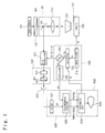
- Fig. 1 is a block diagram showing the arrangement of a voltage measurement apparatus according to the first embodiment of the present invention.
- Figs. 2A to 2H are charts for explaining the operation of the voltage measurement apparatus according to the first embodiment of the present invention.
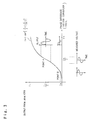
- Fig. 3 is a graph for explaining an optical bias.
- Fig. 4 is a block diagram showing the arrangement of a voltage measurement apparatus according to the second embodiment of the present invention.
- Fig. 5 is a block diagram showing the arrangement of a modification of the voltage measurement apparatus according to the second embodiment of the present invention.
- Fig. 6 is a block diagram showing the arrangement of the 1st comparative apparatus.
- Figs. 7A to 7E are views for explaining the operation of the 1st comparative apparatus.
- Fig. 8 is a block diagram showing the arrangement of the 2nd comparative apparatus.
- Fig. 9 is a graph for explaining the operation of the 2nd comparative apparatus.
- Fig. 1 is a block diagram showing the arrangement of a voltage measurement apparatus according to the first embodiment of the present invention.
- the apparatus of this embodiment comprises (a) a light source 110 for generating a continuous emission light beam, (b) a polarizer 120 for receiving the light beam output from the light source 110, selecting a component of the first polarization direction (X direction in Fig.
- an optical system 140 for focusing the probe light beam output from the polarizer 120
- an E-O probe 200 which is arranged at a position almost matching the focus position of the optical system 140, and has a member consisting of an electro-optic material having an electro-optic effect and a reflection-processed bottom surface on a target measurement portion 710 side
- a drive unit 300 for driving a sample 700 to be measured e.g., a device such as an IC chip or a liquid crystal display panel
- a frequency f 0 e.g., a device such as an IC chip or a liquid crystal display panel
- a photodetector 510 for receiving the light beam output from the electro-optic optical modulator 410 and outputting a photodetection signal corresponding to the intensity of the received light beam
- a synchronous detection unit 520 for receiving the photodetection signal output from the photodetector 510, selecting the component of the frequency ⁇ f, at the same time receiving the signal of the frequency ⁇ f output from the drive unit 300, synchronously detecting the selected photodetection signal in synchronism with the signal of the frequency ⁇ f output from the drive unit 300, and outputting 1 an amplitude detection signal representing the amplitude of the component of the frequency ⁇ f of the photodetection signal output from the photodetector 510, and 2 a phase detection signal representing the phase difference between the signal of the component of the frequency ⁇ f of the photodetection signal output from the photodetector 510 and the signal of the frequency ⁇ f output from the drive unit, and (j) a processing unit
- the optical system 140 has 1 a half mirror 141 for transmitting and outputting part of the probe light beam output from the polarizer 120 and reflecting and outputting part of the light beam reflected by the E-O probe 200, which is input in a direction opposite to the transmission output direction of the probe light beam, toward the electro-optic optical modulator 410, and 2 a focusing lens 142 for focusing the probe light beam transmitted through the half mirror 141.
- the drive unit 300 has 1 a drive device 310 for outputting a drive signal for driving the sample 700 at the frequency f 0 , and outputting a trigger signal having the frequency f 0 , 2 a frequency multiplier 320 for receiving the trigger signal output from the drive device 310, and receiving the notification of the designated number N output from the processing unit 600 to generate a signal of the frequency N ⁇ f 0 obtained by multiplying the designated number N by the frequency f 0 , 3 an oscillator 330 for generating the signal of a frequency ⁇ f 0 , and 4 a mixer 340 for receiving the signal output from the frequency multiplier 320 and the signal output from the oscillator 330, and generating a signal of a frequency N ⁇ f 0 + ⁇ f corresponding to the sum of the frequency N ⁇ f 0 and the frequency ⁇ f.
- the selection unit 420 has 1 a wave plate 421 for receiving the modulated light beam output from the electro-optic optical modulator 410, adjusting the phase, and outputting the light beam, and 2 an analyzer 422 for receiving the light beam through the wave plate 421 and selecting and outputting the polarized light component of the Y direction.
- the synchronous detection unit 520 has 1 a filter 521 for receiving the photodetection signal output from the photodetector 510 and selecting the component of the frequency ⁇ f, and 2 a synchronous detector 522 for receiving the signal output from the filter 521 and the signal of the frequency ⁇ f output from the drive unit 300, detecting the signal output from the filter 521 in synchronism with the signal of the frequency ⁇ f output from the drive unit 300, and outputting i) an amplitude detection signal representing the amplitude of the component of the frequency ⁇ f of the photodetection signal output from the photodetector 510, and ii) a phase detection signal representing the phase difference between the signal of the component of the frequency ⁇ f of the photodetection signal output from the photodetector 510 and the signal of the frequency ⁇ f output from the drive unit.
- a narrow band width detector such as a network analyzer, a spectrum analyzer, and a lock-in amplifier can be preferably employed.
- the apparatus of this embodiment measures a voltage signal waveform at the target measurement position 710 of the sample 700 in the following manner.
- Figs. 2A to 2H are charts showing the operation of the apparatus of this embodiment.
- the drive unit 300 supplies a drive signal of the frequency f 0 to the sample 700 and supplies a modulation signal of the frequency N ⁇ f 0 + ⁇ f to the electro-optic optical modulator 410.
- a continuous light beam is emitted from the light source 110 and incident on the E-O probe 200 through the polarizer 120 and the first optical system 140.
- a periodical voltage waveform is generated at the target measurement portion near the arrangement position of the E-O probe 200 at a fundamental period 1/f 0 .
- Fig. 3 is a graph for explaining the optical bias applied by the wave plate.
- a 1/4 wave plate is used to set the optical bias to a point A in Fig. 3. With this setting, the maximum output change can be obtained with respect to the output from the analyzer 422. In this case, however, a DC output as large as I 1 /2 is also output together with the modulation output, and shot noise is generated due to this DC output.
- the wave plate 421 may be selected to optimize the optical bias, thereby obtaining a satisfactory S/N ratio.
- 0, 1,.8) This photodetection signal is input to the synchronous detection unit 520, and the component of the frequency ⁇ f is heterodyne-detected.
- the synchronous detection signal is acquired and stored as data corresponding to each designated number N. Acquisition and storing are continued until the designated number N for allowing the value of the synchronous detection signal to be regarded as almost zero is reached, or until the limit frequency for the modulation capability of the electro-optic optical modulator is reached.
- the arithmetic unit 610 of the processing unit 600 Upon completion of acquisition and storing, the arithmetic unit 610 of the processing unit 600 reproduces the waveform of the voltage signal generated at the target measurement portion by calculation of Fourier transform on the basis of the stored data and displays the reproduction result on a display unit 620.
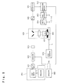
- Fig. 4 is a block diagram showing the arrangement of a voltage measurement apparatus according to the second embodiment of the present invention.
- the apparatus of this embodiment measures the two-dimensional voltage distribution of a target measurement portion.
- the apparatus of this embodiment differs from that of the first embodiment in that a collimator lens 111 and a collimator lens 143 are arranged between a light source 110 and a polarizer 120 and between a focusing lens 142 and an E-O probe 200, respectively, to form an imaging optical system, an imaging system 450 consisting of a lens 451 and a lens 452 is arranged after an analyzer 422, and a two-dimensional photodetector 550 is employed as a photodetector.
- a processing unit a processing unit 650 having an arithmetic unit 651 is employed.
- a high-speed read CCD image sensor capable of performing a high-speed read operation is used.
- a general two-dimensional photodetector such as a photodiode array, an imaging tube, a normal CCD image sensor, or a linear array sensor can also be used.
- a light beam emitted from the light source 110 is collimated and incident on the E-O probe 200, and reflected.
- the two-dimensional image of the reflecting portion is formed, input to the two-dimensional photodetector 550, and converted to a two-dimensional photodetection signal.
- the processing unit 650 acquires and stores a synchronous detection signal at each measurement point, and reproduces the voltage waveform at each measurement point upon completion of acquisition and storing.
- an electro-optic optical modulator 410 must perform modulation throughout an area larger than that in the first embodiment.
- this apparatus can be easily realized because only the uniformity is required.
- the modulation area can be reduced, as in the first embodiment.
- a continuous emission light beam is employed, and after the continuous light beam is influenced by the voltage generated in the sample, modulation and heterodyne detection are performed. Therefore, an accurate voltage measurement apparatus which has a wide frequency band width and needs no short-pulse light source can be realized.
Landscapes
- Engineering & Computer Science (AREA)
- Physics & Mathematics (AREA)
- Electromagnetism (AREA)
- Microelectronics & Electronic Packaging (AREA)
- Health & Medical Sciences (AREA)
- Computer Vision & Pattern Recognition (AREA)
- Computer Hardware Design (AREA)
- Toxicology (AREA)
- General Engineering & Computer Science (AREA)
- General Physics & Mathematics (AREA)
- Measurement Of Current Or Voltage (AREA)
- Tests Of Electronic Circuits (AREA)
- Testing Or Measuring Of Semiconductors Or The Like (AREA)
- Measuring Instrument Details And Bridges, And Automatic Balancing Devices (AREA)
- Investigating Or Analysing Materials By Optical Means (AREA)
Applications Claiming Priority (2)
| Application Number | Priority Date | Filing Date | Title |
|---|---|---|---|
| JP19252/95 | 1995-02-07 | ||
| JP01925295A JP3500215B2 (ja) | 1995-02-07 | 1995-02-07 | 電圧測定装置 |
Publications (2)
| Publication Number | Publication Date |
|---|---|
| EP0726470A2 true EP0726470A2 (de) | 1996-08-14 |
| EP0726470A3 EP0726470A3 (de) | 1997-02-26 |
Family
ID=11994239
Family Applications (1)
| Application Number | Title | Priority Date | Filing Date |
|---|---|---|---|
| EP96300809A Withdrawn EP0726470A3 (de) | 1995-02-07 | 1996-02-07 | Elektrooptische Spannungsmessvorrichtung |
Country Status (3)
| Country | Link |
|---|---|
| US (1) | US5625296A (de) |
| EP (1) | EP0726470A3 (de) |
| JP (1) | JP3500215B2 (de) |
Families Citing this family (3)
| Publication number | Priority date | Publication date | Assignee | Title |
|---|---|---|---|---|
| US6269337B1 (en) * | 1998-07-24 | 2001-07-31 | At&T Corp | Method and apparatus to provide enhanced directory assistance information in a communication network |
| WO2014119676A1 (ja) | 2013-02-01 | 2014-08-07 | 浜松ホトニクス株式会社 | 半導体デバイス検査装置及び半導体デバイス検査方法 |
| JP6283501B2 (ja) * | 2013-11-12 | 2018-02-21 | 浜松ホトニクス株式会社 | 周波数解析装置及び周波数解析方法 |
Citations (4)
| Publication number | Priority date | Publication date | Assignee | Title |
|---|---|---|---|---|
| EP0299432A2 (de) * | 1987-07-13 | 1989-01-18 | Hamamatsu Photonics K.K. | Anordnung eines Spannungsdetektors |
| EP0410234A2 (de) * | 1989-07-22 | 1991-01-30 | Asea Brown Boveri Aktiengesellschaft | Verfahren zur Messung eines elektrischen Feldes oder einer elektrischen Spannung und Einrichtung zur Durchführung des Verfahrens |
| EP0506358A2 (de) * | 1991-03-26 | 1992-09-30 | Hamamatsu Photonics K.K. | Optischer Spannungsdetektor |
| EP0581556A2 (de) * | 1992-07-28 | 1994-02-02 | Hewlett-Packard Company | Berührungslose Test-Sonde und Vorrichtung zur berührungslosen Spannungsmessung |
Family Cites Families (7)
| Publication number | Priority date | Publication date | Assignee | Title |
|---|---|---|---|---|
| US4446425A (en) * | 1982-02-12 | 1984-05-01 | The University Of Rochester | Measurement of electrical signals with picosecond resolution |
| US4618819A (en) * | 1984-03-27 | 1986-10-21 | The University Of Rochester | Measurement of electrical signals with subpicosecond resolution |
| JP2651682B2 (ja) * | 1987-11-05 | 1997-09-10 | 浜松ホトニクス株式会社 | 電圧検出方法 |
| US5057771A (en) * | 1990-06-18 | 1991-10-15 | Tetronix, Inc. | Phase-locked timebase for electro-optic sampling |
| JP3015903B2 (ja) * | 1990-10-23 | 2000-03-06 | 日本電信電話株式会社 | 集積回路の回路試験装置および回路試験方法 |
| US5412330A (en) * | 1993-06-16 | 1995-05-02 | Tektronix, Inc. | Optical module for an optically based measurement system |
| JP3352239B2 (ja) * | 1994-08-19 | 2002-12-03 | 浜松ホトニクス株式会社 | 電圧測定装置 |
-
1995
- 1995-02-07 JP JP01925295A patent/JP3500215B2/ja not_active Expired - Fee Related
-
1996
- 1996-02-06 US US08/597,226 patent/US5625296A/en not_active Expired - Fee Related
- 1996-02-07 EP EP96300809A patent/EP0726470A3/de not_active Withdrawn
Patent Citations (4)
| Publication number | Priority date | Publication date | Assignee | Title |
|---|---|---|---|---|
| EP0299432A2 (de) * | 1987-07-13 | 1989-01-18 | Hamamatsu Photonics K.K. | Anordnung eines Spannungsdetektors |
| EP0410234A2 (de) * | 1989-07-22 | 1991-01-30 | Asea Brown Boveri Aktiengesellschaft | Verfahren zur Messung eines elektrischen Feldes oder einer elektrischen Spannung und Einrichtung zur Durchführung des Verfahrens |
| EP0506358A2 (de) * | 1991-03-26 | 1992-09-30 | Hamamatsu Photonics K.K. | Optischer Spannungsdetektor |
| EP0581556A2 (de) * | 1992-07-28 | 1994-02-02 | Hewlett-Packard Company | Berührungslose Test-Sonde und Vorrichtung zur berührungslosen Spannungsmessung |
Also Published As
| Publication number | Publication date |
|---|---|
| JP3500215B2 (ja) | 2004-02-23 |
| US5625296A (en) | 1997-04-29 |
| JPH08211131A (ja) | 1996-08-20 |
| EP0726470A3 (de) | 1997-02-26 |
Similar Documents
| Publication | Publication Date | Title |
|---|---|---|
| US5767688A (en) | Electro-optic voltage measurement apparatus | |
| JP3364333B2 (ja) | 減衰特性測定装置 | |
| US5905577A (en) | Dual-laser voltage probing of IC's | |
| US6876441B2 (en) | Optical sensor for distance measurement | |
| US5179565A (en) | Low noise pulsed light source utilizing laser diode and voltage detector device utilizing same low noise pulsed light source | |
| EP0197196A1 (de) | Elektro-elektronenoptisches Oszilloskop zur Zeitauflösung elektrischer Wellenzüge im Picosekundenbereich | |
| US5579103A (en) | Optical radar ranger with modulation of image sensor sensitivity | |
| JP2004527765A5 (de) | ||
| US5625296A (en) | Electro-optic voltage measurement apparatus | |
| US5847570A (en) | Low jitter trigger circuit for electro-optic probing apparatus | |
| US5666062A (en) | Voltage measuring using electro-optic material's change in refractive index | |
| JP3352543B2 (ja) | 電圧測定装置 | |
| JP2847289B2 (ja) | 距離形状測定装置 | |
| JP3352244B2 (ja) | 電圧測定装置 | |
| JP3165873B2 (ja) | 電気信号測定方法および装置 | |
| EP0506358A2 (de) | Optischer Spannungsdetektor | |
| US7218402B1 (en) | Wavefront sensor using hybrid optical/electronic heterodyne techniques | |
| JP3549813B2 (ja) | 高周波電磁波検出システム及び高周波電磁波検出方法 | |
| JPH0522216B2 (de) | ||
| JPH04121673A (ja) | 光サンプリング装置 | |
| EP0307936B1 (de) | Vielkanalspannungsdetektor | |
| Musch et al. | A multiple target high precision laser range measurement system based on the FMCW concept | |
| JP5219023B2 (ja) | 電界、電圧または磁界用測定プローブ | |
| JPH036465A (ja) | レーザ光を用いた非接触型電圧測定装置 |
Legal Events
| Date | Code | Title | Description |
|---|---|---|---|
| PUAI | Public reference made under article 153(3) epc to a published international application that has entered the european phase |
Free format text: ORIGINAL CODE: 0009012 |
|
| AK | Designated contracting states |
Kind code of ref document: A2 Designated state(s): DE FR GB |
|
| PUAL | Search report despatched |
Free format text: ORIGINAL CODE: 0009013 |
|
| AK | Designated contracting states |
Kind code of ref document: A3 Designated state(s): DE FR GB |
|
| 17P | Request for examination filed |
Effective date: 19970822 |
|
| 17Q | First examination report despatched |
Effective date: 20010405 |
|
| STAA | Information on the status of an ep patent application or granted ep patent |
Free format text: STATUS: THE APPLICATION IS DEEMED TO BE WITHDRAWN |
|
| 18D | Application deemed to be withdrawn |
Effective date: 20010816 |