EP0725535A2 - Solid-state image pickup device - Google Patents
Solid-state image pickup device Download PDFInfo
- Publication number
- EP0725535A2 EP0725535A2 EP96300696A EP96300696A EP0725535A2 EP 0725535 A2 EP0725535 A2 EP 0725535A2 EP 96300696 A EP96300696 A EP 96300696A EP 96300696 A EP96300696 A EP 96300696A EP 0725535 A2 EP0725535 A2 EP 0725535A2
- Authority
- EP
- European Patent Office
- Prior art keywords
- output
- signals
- pixels
- image pickup
- photoelectric conversion
- Prior art date
- Legal status (The legal status is an assumption and is not a legal conclusion. Google has not performed a legal analysis and makes no representation as to the accuracy of the status listed.)
- Granted
Links
- 239000000872 buffer Substances 0.000 claims abstract description 55
- 238000006243 chemical reaction Methods 0.000 claims abstract description 45
- 238000012546 transfer Methods 0.000 claims description 49
- 238000009825 accumulation Methods 0.000 claims description 48
- 238000000034 method Methods 0.000 claims description 29
- 230000008569 process Effects 0.000 claims description 27
- 230000008878 coupling Effects 0.000 claims description 17
- 238000010168 coupling process Methods 0.000 claims description 17
- 238000005859 coupling reaction Methods 0.000 claims description 17
- 238000007781 pre-processing Methods 0.000 claims description 14
- 238000012545 processing Methods 0.000 claims description 6
- 238000012935 Averaging Methods 0.000 claims description 4
- 230000003287 optical effect Effects 0.000 claims 3
- 230000035508 accumulation Effects 0.000 description 41
- 238000010586 diagram Methods 0.000 description 17
- 230000000694 effects Effects 0.000 description 13
- 238000001514 detection method Methods 0.000 description 8
- 244000045947 parasite Species 0.000 description 7
- 238000007667 floating Methods 0.000 description 5
- 230000035945 sensitivity Effects 0.000 description 5
- 230000003321 amplification Effects 0.000 description 4
- 230000006872 improvement Effects 0.000 description 4
- 230000001678 irradiating effect Effects 0.000 description 4
- 238000003199 nucleic acid amplification method Methods 0.000 description 4
- 230000004044 response Effects 0.000 description 4
- 230000000717 retained effect Effects 0.000 description 4
- 230000003139 buffering effect Effects 0.000 description 3
- 238000004364 calculation method Methods 0.000 description 2
- 239000000969 carrier Substances 0.000 description 2
- 230000004048 modification Effects 0.000 description 2
- 238000012986 modification Methods 0.000 description 2
- 230000009467 reduction Effects 0.000 description 2
- 230000015572 biosynthetic process Effects 0.000 description 1
- 239000003990 capacitor Substances 0.000 description 1
- 230000007423 decrease Effects 0.000 description 1
- 230000001419 dependent effect Effects 0.000 description 1
- 238000011161 development Methods 0.000 description 1
- 230000018109 developmental process Effects 0.000 description 1
- 230000008030 elimination Effects 0.000 description 1
- 238000003379 elimination reaction Methods 0.000 description 1
- 238000005516 engineering process Methods 0.000 description 1
- 238000004519 manufacturing process Methods 0.000 description 1
- 230000006798 recombination Effects 0.000 description 1
- 238000005215 recombination Methods 0.000 description 1
- 238000009877 rendering Methods 0.000 description 1
- 239000004065 semiconductor Substances 0.000 description 1
- 230000004304 visual acuity Effects 0.000 description 1
Images


Classifications
-
- H—ELECTRICITY
- H04—ELECTRIC COMMUNICATION TECHNIQUE
- H04N—PICTORIAL COMMUNICATION, e.g. TELEVISION
- H04N25/00—Circuitry of solid-state image sensors [SSIS]; Control thereof
-
- H—ELECTRICITY
- H04—ELECTRIC COMMUNICATION TECHNIQUE
- H04N—PICTORIAL COMMUNICATION, e.g. TELEVISION
- H04N25/00—Circuitry of solid-state image sensors [SSIS]; Control thereof
- H04N25/70—SSIS architectures; Circuits associated therewith
- H04N25/701—Line sensors
-
- H—ELECTRICITY
- H04—ELECTRIC COMMUNICATION TECHNIQUE
- H04N—PICTORIAL COMMUNICATION, e.g. TELEVISION
- H04N25/00—Circuitry of solid-state image sensors [SSIS]; Control thereof
- H04N25/70—SSIS architectures; Circuits associated therewith
- H04N25/76—Addressed sensors, e.g. MOS or CMOS sensors
-
- H—ELECTRICITY
- H04—ELECTRIC COMMUNICATION TECHNIQUE
- H04N—PICTORIAL COMMUNICATION, e.g. TELEVISION
- H04N25/00—Circuitry of solid-state image sensors [SSIS]; Control thereof
- H04N25/70—SSIS architectures; Circuits associated therewith
- H04N25/76—Addressed sensors, e.g. MOS or CMOS sensors
- H04N25/767—Horizontal readout lines, multiplexers or registers
Definitions
- the present invention relates to a solid-state image pickup device.
- the solid-state image pickup device represented by the CCD has shown significant improvement in performance and has been applied in various products such as facsimile and scanner.
- there are emerging stronger requirements for the solid-state image pickup device not only for a higher performance such as a higher sensitivity or a higher resolving power, but also for drivability with a lower voltage.
- products drivable with a 5 V power source there have appeared products drivable with a 5 V power source and developments are being made to achieve drivability with a lower voltage.
- Fig. 1 is an equivalent circuit diagram of a unit pixel, which is composed of an NPN bipolar phototransistor 14, a pixel separating-resetting PMOS transistor 11, a base potential control capacitor 13, a three-value pulse supply terminal PR, and a bias reset supply terminal VBR.
- Fig. 2 shows a solid-state image pickup device consisting of a one-dimensional array of four bipolar photoelectric converting elements explained above, while a three-value pulse from a three-pulse terminal 1 is in the LOW level state, a reset pulse is supplied from a reset terminal 2 to render the PMOS transistors 11 conductive, whereby the NPN transistors 14 are reset.
- the gate-source voltage VGS of the PMOS transistors 11-1 to 11-4 becomes lower than the threshold value Vth of the transistors, whereby these transistors are rendered non-conductive and a first resetting operation is completed.
- the reset terminal 33 when the reset terminal 33 is shifted to the high level state, the NMOS transistors 22 are rendered conductive and the emitters of the NPN transistors 14 are reset. Subsequently the three-value pulse terminal 1 is shifted to the high level state, whereby the bases of the NPN transistors 14 are shifted to the floating state through the control capacitances 13, and, when the three-value terminal 1 is shifted to the middle level, there is initiated the accumulation of the photon charges by photoelectric conversion.
- a transfer terminal 32 and the three-value pulse terminal 1 are shifted to the high level state, whereby the NMOS transistors 23 are rendered conductive, and the charges accumulated in the bases are transferred to transfer capacitances 24 by the application of a high-level pulse to the reset terminal 3.
- a reset pulse is applied to the reset terminal 27 whereby the remaining charge on the output line 42 is dissipated to the ground through an NMOS transistor 26.
- the image of a line can be released through the above-explained operations, and the function as an area sensor can be achieved by repeating the above-explained operations in combination with a movement of the sensor.
- the signals of the different pixels are once read into the transfer capacitances C24-1 to C24-4 and are then serially transferred to the output terminal by the function of the scanning circuit.
- the capacitance CH is composed of the drain capacitance and the gate overlapping capacitance of the scanning transistors 25-1 to 25-4 and the resetting transistor 26, the input capacitance of the output amplifier and the parasite capacitance of the output wiring, and is heavily dependent on the number of pixels and the manufacturing process. It is in the order of several picofarads in case of several hundred pixels.
- CT is composed of the capacitances of the MOS device and of junctions, and is designed in the order of several picofarads in the actual integrated circuit.
- the image taking will not be required if the brightness of the image is low and does not reach the sensitivity of the pixels, but, if the image has a certain level of brightness, it is often required to obtain details of such lighted area.
- the image detection with a line sensor under such condition requires the scanning operation over the entire pixels, thus requiring a long time for the scanning operation with a large power consumption, and, if such brightness appears instantaneously, it is difficult to detect such instantaneous bright area.
- the time for one cycle is principally used for pixel resetting, signal read-out and serial signal transfer, and the significant part is usually used for the serial transfer.
- This time becomes longer with the increase in the number of pixels, and, in case of an area sensor with plural lines, most of the cycle time is occupied by the signal transfer time. Consequently, in the application for a detector for detecting the presence or absence of an image at a high speed, it is an important issue how to reduce this time.
- the present inventors have disclosed, in the Japanese Patent Laid-open Application No. 6-268920, that this signal transfer time can be reduced by releasing a signal averaged over plural pixels.
- the signal averaging is easy in the horizontal direction of the area sensor, it can normally be made for 2 to 4 pixels in the vertical direction, as a larger averaging leads to an increase in the chip size. Consequently an inexpensive high-speed detector has been extremely difficult to realize with an area sensor.
- An object of the present invention is to provide a solid-state image pickup device provided with an array of plural blocks each of which is composed of two or more pixels, wherein the outputs of said block are connected in common, respectively through amplifier means.
- Another object of the present invention is to provide a solid-state image pickup device capable, for resolving the above-mentioned drawbacks, of outputting both an output signal obtained by pre-processing of the signals of the pixels and an output from each pixel, wherein the above-mentioned pre-processed output signal is output through output means for the signal of each pixel.
- Fig. 3 in which there are shown unit pixels 80 of a photoelectric converting element, pixel buffer means 81 for buffering pixel signals, function circuits 82 such as clamping circuits, and block buffer means 83 for buffering block signals.
- Signals from the pixels 80 are supplied respectively through the pixel buffers 81 and are wire-connected among every three pixels to provide block signals, which are subjected to a suitable signal processing in the function circuits 82 and wire-connected, after passing the block buffers 83, for all the blocks, whereby a signal representing all the blocks is output from an output terminal 84.
- the block buffer means 83 With all the above-mentioned operations are conducted collectively for all the pixels or all the blocks, there is only required an extremely short process time with a reduced power consumption. Also by constituting the block buffer means 83 with bipolar transistors and connecting the emitters thereof in common for all the blocks, the maximum value of the signals of all the blocks can be read out, without loss to the output terminal 84.
- the image read-out in the block form but a higher function of the solid-state image pickup device can be achieved, by reading out the signals of the pixels constituting the blocks as in the conventional solid-state image pickup device. More specifically, the image pickup device is featured by first photoelectric conversion means for reading out photoelectrically converted charge of each pixel and second photoelectric conversion means for reading out photoelectrically converted charge of each block consisting of plural pixels, wherein the outputs of the above-mentioned photoelectric conversion means are connected, through maximum output means, to a common line.
- This configuration will be explained in more details in the following embodiments.
- Fig. 4 illustrates a first embodiment of the present invention, composed of a one-dimensional array of four bipolar photoelectric conversion elements as employed in Fig. 1.
- the NPN transistor 14 serving as the bipolar photoelectric conversion element, the base control capacitance 13 and the resetting PMOS transistor 11 correspond to the pixel 80.
- the emitter of the NPN transistor 14 corresponds to the pixel buffer 81, while the resetting NMOS transistor 12, the transfer NMOS transistor 15 and the transfer capacitance 16 correspond to the function circuit 82, and the NPN transistor 17 and the constant current source 18 correspond to the block buffer 82.
- a block is constituted by the NPN transistors 14-1 and 14-2, while another block is constituted by the NPN transistors 14-3 and 14-4.
- a low level pulse is applied to the three-value pulse terminal 1 to render the PMOS transistors 11-1 to 11-4 conductive, whereby the base areas of the photoelectric conversion elements are reset to a voltage given to the reset terminal 2 (first resetting).
- the pulse to the three-value pulse terminal 1 is shifted to the middle level to shift the gate-source voltage VGS of the PMOS transistors 11-1 to 11-4 to a value not exceeding the transistor threshold voltage Vth, whereby the PMOS transistors are rendered non-conductive and the first resetting operation is completed.
- a high level pulse is applied to the reset pulse terminal 3 to render the NMOS transistors 12-1, 12-2 conductive, whereby the emitters of the pixel NPN transistors 14 are reset to a reset voltage (which is the ground in the illustrated configuration).
- a high level pulse is applied to the three-value pulse terminal 1 to elevate the base potential of the NPN transistors 14 by the capacitative coupling through the base control capacitances 13-1 to 13-4 to generate a forward bias between the bases and the emitters, while the PMOS transistors 11-1 to 11-4 are maintained in the non-conductive state.
- the NPN transistors 14 effect an emitter follower operation whereby the holes on the base areas in the floating state effect recombination and the base potentials are reset (second resetting).
- the pulse to the three-value pulse terminal 1 is lowered to the middle level, whereby the base potentials of the pixels are shifted to the negative side to generate an inverse bias between the bases and the emitters. At this point there is initiated the accumulation of the photoelectrically converted charges in the bases.
- a high level pulse is applied to the transfer terminal 4 to render the NMOS transistors 15-1, 15-2 conductive, whereby the emitters of the NPN transistors 14 of all the pixels are connected to the capacitances 16-1, 16-2 and are at the same time reset to the ground level through the NMOS transistors 12-1, 12-2.
- the pulse to the reset pulse terminal 3 is shifted to the low level to render the NMOS transistors 12-1, 12-2 non-conductive.
- a high level pulse is applied to the three-value pulse terminal 1 to shift the base potentials of all the pixels to the positive side through the capacitances 13-1 to 13-4, whereby a forward bias state is generated between the bases and emitters of the NPN transistors 14-1 to 14-4 of all the pixels.
- the maximum voltages of the signals of the pixels 1, 2 and the pixels 3, 4 are respectively read out into the transfer capacitances 16-1, 16-2.
- the transfer capacitances 16-1, 16-2 are respectively connected to the bases of the NPN transistors 17 of which emitters are connected in common to the output line 2, the maximum voltage of the transfer capacitances 16-1, 16-2 is supplied to the output line 2.
- V0 CT ⁇ hFE ⁇ V1/(CT ⁇ hFE + CH) since the collector current Ic of a transistor is hFE times of the base current Ib. Since hFE of the NPN transistors 17 is usually equal to or higher than 100, the parasite capacitance CH becomes negligible, and the signal readout can be achieved with a gain almost equal to 1.
- the pulse to the transfer terminal 4 is shifted to the low level state to terminate the readout operation, whereupon the transfer capacitances 16-1, 16-2 are maintained in the floating state and the output voltage becomes gradually lower.
- the rate of decline of the output voltage is represented by: IS/(hFE ⁇ CB) wherein IS is the current of a constant current source 18 provided in the output stage, and CB is the base capacitance of the NPN transistors 17-1, 17-2, so that the output period can be made longer by selecting a small constant current IS.
- the foregoing first embodiment employs NPN transistors for the block buffer means, but there may also be employed PNP transistors.
- the bases are connected to the function circuits while the emitters are connected in common to a power source through a constant current source, and the collectors are grounded, and the output is obtained from the commonly connected emitters.
- the minimum potential of the blocks is output.
- inverting the polarity of the foregoing embodiment for example by employing a PNP transistor and an NMOS transistor for each pixel, the charge of a pixel having the minimum charge among all the pixels is output.
- Such configuration for detecting the minimum pixel charge is effective for instantaneous detection of a dark area, generated instantaneously in an extremely bright field.
- the configuration of the present invention can be advantageously utilized as a detector, as it enables high-speed readout of the pixel block signals without loss.
- Figs. 6 and 7 illustrate a second embodiment of the present invention, wherein components equivalent to those in Fig. 4 are represented by same numbers and will not be explained further.
- the present embodiment is an improvement on the first embodiment, and is capable of both the block signal readout of the first embodiment and the readout of the signals of all the pixels.
- the photoelectric conversion element employed in the present embodiment is composed, as shown in Fig. 6, of an NPN transistor 21 with two emitters, a PMOS transistor 11 and capacitance means 13, wherein one of the two emitters is connected with those of other photoelectric conversion elements to constitute a pixel block, thereby outputting the maximum voltage among the pixels constituting the block. And another emitter is connected with a readout circuit as explained in conventional configuration. So that, it is a combination of the conventional configuration shown in Fig. 2 and the first embodiment shown in Fig. 4.
- a low level pulse is applied to the three-value pulse terminal 1 to effect first resetting of the pixels, and, at a time T1, a middle level pulse is applied to the three-value pulse terminal 1 to render the PMOS transistors 11 non-conductive.
- high level pulses are applied to the reset terminal 3 and the terminal 33 to reset the two emitters of the NPN transistor 21 of each pixel to a reset potential (ground in the illustrated configuration).
- a high level pulse is applied to the three-value pulse terminal 1 to effect second resetting through the NMOS transistors 12, 22.
- the pulse to the three-value pulse terminal 1 is lowered to the middle level to terminate the resetting operation and to initiate the accumulation of the photoelectrically converted charges in the bases of the NPN transistors 21.
- a high level pulse is applied to the three-value pulse terminal 1 to transfer the signals of the pixels respectively to the capacitances 24-1 to 24-4 and the highest voltages of the pixels 1, 2 and of the pixels 3, 4 respectively to the capacitances 16-1, 16-2 whereby the highest voltage of the capacitances 16-1, 16-2 is supplied to the output line 2.
- the pulses at the transfer terminals 32, 4 are shifted to the low level whereby the readout operation is terminated.
- the pulse to the three-value pulse terminal 1 is shifted down to the low level, and, at a time T10, a high level pulse is applied to the reset terminal 27 to reset the output line 42.
- a start pulse 30 and scanning pulses 31 are supplied to the scanning circuit 29 respectively at times T11 and T12 whereby the signals of the pixels are time-sequentially read out to the output terminal 28, in synchronization with clock signals.
- the signal of the blocks is read before the readout of the signal of each pixel, but the following drive is also possible for example in the application for a detector.
- the operations of the device can be significantly simplified by at first reading the block signal, then discriminating whether the block signal is larger (or smaller) than a predetermined value, and, if larger (or smaller), reading the signals of every pixels, but, if smaller (or larger), terminating the each signal readout from the pixels because the signal level of the pixels is too low. In this manner it is possible to reduce the process time and to significantly reduce the power consumption.
- Fig. 9 shows a third embodiment of the present invention, wherein components equivalent to those in Fig. 4 are represented by same numbers and will not be explained further.
- the present embodiment is provided, serially to the vertical output lines, with capacitance means 38-1 to 38-4 and capacitance means 36-1, 36-2 to effect clamping operations for the signals, thereby eliminating FPN (fixed pattern noise) and random noises, and also eliminating external light components other than the reflected light, in case of irradiating an object with light from a light source such as an LED and taking the reflected light.
- FPN fixed pattern noise
- an output corresponding to the dark signal can be obtained by selecting an extremely short accumulation time for the first accumulation, so that FPN (fixed pattern noise), which is a drawback of the amplifying solid-state image pickup device, can be eliminated by obtaining the difference between the above-mentioned output and the second output. Also by selecting a same accumulation time for the first and second accumulations and irradiating the object with the light from the light source such as an LED during the second accumulation time, the reflected image of the object can be precisely read out even in a bright indoor situation, and such ability is suitable particularly for a detector.
- FPN fixed pattern noise
- the block signals and the individual pixel signals are also output through the clamping circuits, but such clamping circuits may naturally be dispensed with.
- Fig. 11 shows a fourth embodiment of the present invention, wherein components equivalent to those in Fig. 4 are represented by same numbers and will not be explained further.
- the present embodiment provides an area sensor consisting of a two-dimensional array of the photoelectric conversion elements.
- each block is composed of two pixels in the vertical direction and two pixels in the horizontal direction, and the outputs of the blocks are transferred to transfer capacitances 24-1 to 24-4, while the pixel signals are driven by the output of a vertical shift register.
- the present embodiment providing a larger image pickup area than in the third embodiment, can achieve more precise detecting operation.
- a vertical scanning shift register 43 in response to a start pulse 50 and vertical scanning pulses 51, a vertical scanning shift register 43 sends horizontal scanning pulses in succession to horizontal lines, thereby controlling switches 44-1 to 44-4 including inverters.
- the three-value pulse entered from the three-value pulse terminal 1 is turned on and off by the switches 44 to at first activate the pixels of the 1st and 2nd horizontal scanning lines, composed of the NPN transistors 21-11 to 21-14 and 21-21 to 21-24, whereby the signals of these pixels are transferred to the transfer capacitances 24-1 to 24-4 and are output in succession to the output terminal 28 through the output line 42.
- the charges obtained from the NPN transistors 21-11, 21-12, 21-21 and 21-22 are transferred to a coupling capacitance 36-2 while those obtained from the NPN transistors 21-13, 21-14, 21-23 and 21-24 are transferred to a coupling capacitance 36-4 and then transferred to transfer capacitances 16-2, 16-4, whereby a voltage corresponding to the maximum charge in the blocks are obtained at the output terminal 5.
- each block is composed of 2 ⁇ 2 pixels, but there may employed a larger number of pixels for constituting a block.
- a larger number of pixels improves the S/N ratio of the output at the output terminal 5 and enables image readout at a higher speed, thereby enabling image pickup with a higher precision, in combination with the readout of the pixel signals.
- the signal of each block is detected with a peak signal, obtained from NPN transistors, but it is also possible to detect a bottom signal with PNP transistors, and both may be employed in combination for achieving finer detection.
- the 1st to 4th embodiments have the following technological advantages.
- Enabling high-speed readout of the pixel block signal without loss are advantageously applicable to detectors. It is also possible to significantly simplify the operation, in certain applications such as for detector, to at first read out the block signal, then to discriminate whether such block signal is larger (or smaller) than a predetermined value, and, if it is larger (or smaller), to read out the pixel signals in succession, but, if it is smaller (or larger), to terminate the signal readout as the level of the pixel signals is too low. In this manner it is rendered possible to reduce the process time and the power consumption.
- the utilization of the block signal there can be obtained an output corresponding to a dark area by selecting a very short first accumulation time, and the FPN (fixed pattern noise), which is a drawback of the amplifying solid-state image pickup device, can be eliminated by obtaining the difference between the above-mentioned output and the second output. Also by selecting a same accumulation time for the first and second accumulating operations and irradiating the object with the light from a light source such as an LED in the course of the second accumulating time, the reflected image of the object can be read out in highly precise manner even in a bright indoor situation. Such function can be advantageously utilized particularly in a detector.
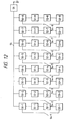
- a 5th embodiment wherein shown are unit pixels 51-1 to 51-8; transfer means 50-1 to 50-8 for retaining the pixel signals of the unit pixels 51-1 to 51-8 in accumulating capacitances and then serially outputting the pixel signals to an output line 55; pre-process means 52-1 to 52-8 connected to the unit pixels 51-1 to 51-8 for effecting a pre-process; buffer means 53-1 to 53-8 for buffering the signals from the pro-process means; and switching means 54-1 to 54-8 connecting the transfer means 50-1 to 50-8 with the buffer means 53-1 to 53-8.
- the buffer means 53-1 to 53-8 may be dispensed with if unnecessary.
- the signals of the unit pixels 51-1 to 51-8 are transferred to the transfer means 50-1 to 50-8 for retaining the signal of each pixel, and are output to a terminal 57 through an output line 55 and an output circuit 56. Also they are subjected to a suitable pre-processing in the pre-process means 52-1 to 52-8, then transferred to the transfer means 50-1 to 50-8 through the buffer means 53-1 to 53-8, and released to the terminal 57. Naturally the unprocessed signals and the pre-processed signals have to be released in different periods. It is also possible to form the unprocessed signals and the pre-processed signals into blocks in the transfer means 50-1 to 50-8 and to output these signals by serial transfer after mixing thereof.
- the transfer means 50-1 to 50-8 can be realized, for example, by the accumulating capacitances 24-1 to 24-4, the switch means 25-1 to 25-4 and the scanning circuit 29 shown in Fig. 2, and the pre-process circuit can be composed of an FPN (fixed pattern noise) elimination circuit utilizing a clamping circuit to be explained later.
- FPN fixed pattern noise
- the signals pro-processed in the pre-process means 52-1 to 52-8 are buffered by the buffer means 53-1 to 53-8, and plural columns are formed into a block, of which signal is transferred to retain/transfer means.
- This configuration allows to reduce the amount of pixel signals and to significantly reduce the cycle time, and the retain/transfer circuits and the output circuit can be used in common for the unprocessed signals, so that a major increase in the chip size is not required.
- Fig. 14 shows a 6th embodiment of the present invention, employing four bipolar photoelectric conversion elements shown in Fig. 1, arranged in a linear array.
- components equivalent to those in Fig. 2 are represented by same numbers.
- the present embodiment is provided, as explained in the foregoing embodiment shown in Fig. 12, with pre-processing means composed of coupling capacitances 105-1 to 105-4 and NMOS transistors 106-1 to 106-4; buffer means composed of buffer capacitances 107-1 to 107-4 and NMOS transistors 109-1 to 109-4; and switch means composed of NMOS transistors 116-1 to 116-4.
- a low level pulse is supplied to a terminal 201 to render the PMOS transistors 101-1 to 101-4 conductive whereby the base areas of the photoelectric conversion elements are reset to a voltage given to a terminal 202 (first resetting). Then the pulse to the terminal 201 is shifted to the middle level to reduce the gate-source voltage VGS of the PMOS transistors 101-1 to 101-4 to a value not exceeding the threshold value Vth thereof, whereby these PMOS transistors are rendered non-conductive and the first resetting operation is completed.
- a high level pulse is applied to a terminal 206 to render the NMOS transistors 110-1 to 110-4 conductive, whereby the emitter of the NPN transistors of the pixels is reset to a reset potential (ground in the illustrated configuration).
- a high level pulse is applied to the terminal 201 to elevate the base potential of the NPN transistors by the capacitative coupling through the capacitances 102-1 to 102-4 thereby generating a forward bias between the bases and the emitters, while the PMOS transistors 101-1 to 101-4 are retained in the non-conductive state, whereby the NPN transistors 103-1 to 103-4 effect an emitter follower operation.
- the holes on the base areas in the floating state effect photorecombination and the base potential is reset (second resetting operation).
- the pulse to the terminal 201 is shifted down to the middle level to shift the base potentials of the pixels to the negative side, whereby an inverse bias state is generated between the bases and the emitters and an accumulating operation is thereby initiated (first accumulating operation).
- the pulse to the terminal 206 is shifted down to the low level state to render the NMOS transistors 110-1 to 110-4 non-conductive, whereby the emitters of the pixel transistors 103-1 to 103-4 and the capacitances 112-1 to 112-4 are shifted to a floating state.
- a high level pulse is applied to a terminal 201 to shift the base potentials of the pixels to the positive side through the capacitances 102-1 to 102-4, thereby generating a forward bias between the bases and emitters of the NPN transistors 103-1 to 103-4 of the pixels. Consequently the signals obtained by photoelectric conversion in the respective pixels and accumulated in the base areas are respectively transferred to the accumulation capacitances 112-1 to 112-4 and the coupling capacitances 105-1 to 105-4.
- the pulse to the terminal 205 is shifted down to render the NMOS transistors 109-1 to 109-4 non-conductive.
- the pulse to the terminal 201 is shifted down to turn off the NPN transistors 103-1 to 103-4 through the capacitances 102-1 to 102-4 whereby the readout operation is terminated.
- a high level pulse is applied to the terminal 206 to reset the accumulation capacitances 112-1 to 112-4 again, and, at a time T17, a high level pulse is applied to a terminal 213 to render the NMOS transistors 116-1 to 116-4 conductive, whereby the signals in the buffer capacitances 107-1 to 107-4 are transferred to the accumulation capacitances 112-1 to 112-4.
- the terminals 204, 207 are shifted to the low level state to turn off the NMOS transistors 106-1 to 106-4 and 111-1 to 111-4, whereby the NMOS transistors 116-1 to 116-4 are rendered non-conductive.
- a scanning circuit 130 is activated with the resetting of an output line 140, thereby serially transferring the signals of the accumulation capacitances 112-1 to 112-4 to an output terminal 211, and the operations of a series are thus completed. It is also possible to eliminate the FPN (fixed pattern noise) in these operations, by selecting a very short first accumulation time to obtain a signal corresponding to the dark area, and calculating the difference of the above-mentioned signal and the signal obtained in the second accumulation.
- FPN fixed pattern noise
- the unprocessed signals may also be obtained according to a timing chart shown in Fig. 16.
- the terminal 213 is always maintained at the low level state, whereby the NMOS transistors 115-1 to 115-4 are always in the non-conductive state. Consequently the calculation in the clamping circuits does not at all affect the accumulation capacitances 112-1 to 112-4, so that, in the readout operation, the pixel signals are directly read out to the accumulation capacitances 112-1 to 112-4 as in the conventional configuration, and they are not reset but are serially output by the scanning circuit 130.
- Such direct readout of the sensor signals is effective for improving the detecting sensitivity, for example in case of detecting an object of relatively low luminance, as in an indoor situation, since the clamping process reduces the output as represented by the equation (4).
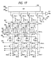
- the pre-processing circuit is composed of a difference calculating circuit utilizing a clamping circuit, but it is also possible, as shown in Fig. 17, to effect signal averaging among the adjacent pixels as the pre-processing, by providing retaining capacitances 118-1 to 118-8, grouped by two and connected respectively to the vertical output lines through switch means 117-1 to 117-4, also providing switch means for connecting the retaining capacitances between the adjacent pixels and connecting the outputs of these switch means to the emitters of the NPN transistors 103-1 to 103-4 through transfer switches 116-1 to 116-4.
- the pre-processing circuit may be composed of a calculation circuit utilizing an operational amplifier.
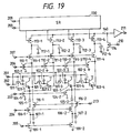
- Fig. 19 shows a 7th embodiment of the present invention, wherein components equivalent to those in Figs. 1 to 18 are represented by same numbers and will not be explained further.
- the photoelectric conversion element employed in the present embodiment is similar to that shown in Fig. 6.
- One of the two emitters is connected in common among the pixels constituting a pixel block, whereby the maximum voltage of the pixels constituting the block is accumulated in either of the buffer capacitances 107-1, 107-2. Such maximum voltages are transferred to the accumulation capacitances 112-1, 112-3 and output from the terminal 211 through the function of the scanning circuit 130.
- the driving method of the present embodiment is similar to that explained in Fig. 15 or 16, whereby the terminal 203 is driven simultaneously with the terminal 206 to effect resetting and accumulation. Consequently, the output of each block representing the highest output level within the block, is read out, and the detecting operation is executed by this output in the ordinary state. It is also possible, based on the result of such detecting operation, to read out the signals of every pixels if necessary. As there is obtained the output of the pixel of highest output level among the plural pixels within the block, there can be achieved an improvement in the detecting precision and a significant reduction in the amount of signals, leading to a reduced cycle time and a reduction in the power consumption.
- Fig. 20 shows an 8th embodiment of the present invention, wherein components equivalent to those in Figs. 1 to 19 are represented by same numbers and will not be explained further.
- the present embodiment corresponding to an improvement on the 7th embodiment, is provided the buffer capacitances 107-1, 107-2 at the output of the clamping circuits, with NPN transistors 108-1, 108-2 of which emitters are connected in common and further connected to a constant current source 115 and an output terminal 212.
- the maximum value of the signals transferred to the buffer capacitances 107-1, 107-2 is immediately output to the terminal 212 without the function of the scanning circuit 130, so that the cycle time and the power consumption can be further reduced in comparison with the 7th embodiment.
- the NPN transistors employed in the present embodiment there may be employed PNP transistors in emitter follower circuits to provide the minimum value of the block signals at the terminal 212. Consequently the present embodiment can achieve a function of detecting whether the signal is higher (or lower) than a predetermined level and then reading out the signals of the blocks or pixels based on the result of such detection according to the need so that the photoelectrically converted output can be obtained, matching the intention of photoelectric conversion.
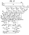
- the buffer capacitances 107-1, 107-2 are reset to the ground potential by the NMOS transistors 109-1 and 109-2, but it is more effective for reading out small output voltages, as shown in Fig. 21, by providing a reset power source terminal 231 in order to generate a sufficient forward bias voltage between the bases and the emitters of the NPN transistors 108-1, 108-2.
- the signals of the buffer capacitances 107-1, 107-2 are read out by the emitter follower circuits utilizing the constant current source 115, so that the signal voltage of the buffer capacitance declines, during a readout time TR, by: ⁇ (IO/ ⁇ ) ⁇ TR ⁇ /CB wherein ⁇ is the current amplification factor of the NPN transistors 108-1, 108-2, I0 is the current of the constant current source 115, and CB is the capacity of the buffer capacitance.
- ⁇ is the current amplification factor of the NPN transistors 108-1, 108-2
- I0 is the current of the constant current source 115
- CB is the capacity of the buffer capacitance.
- Such loss in the signal voltage can be reduced to: ⁇ (IO/ ⁇ 2 ) ⁇ TR ⁇ /CB by employing Darlington emitter follower circuits as shown in Fig. 22, and can be brought to practically zero, by selecting a current amplification factor ⁇ of ca. 1000, an I0 of several
- Fig. 23 shows a 9th embodiment of the present invention, wherein components equivalent to those in Figs. 1 to 22 are represented by same numbers and will not be explained further.
- the buffer capacitances 107-1 to 107-4 and the accumulation capacitances 112-1 to 112-4 are connected through the switches 116-1 to 116-4, so that the transfer gain, represented by: C T /(C T + C T2 + C S2 ) is in the order of 0.3 to 0.4, wherein:
- the buffer capacitances 107-1, 107-2 are provided with emitter follower circuits utilizing NPN transistors 108-1, 108-2 and the outputs thereof are connected to the accumulation capacitances 112-1, 112-3 through the switches 116-1, 116-2. Consequently, as regardless of the capacity of the parasite capacitance C S2 the signals can be transferred to the accumulation capacitances 112-1 to 112-4 almost without loss. Such configuration is effective in case the signals from the sensors are small.
- Fig. 24 shows a 10th embodiment of the present invention, wherein components equivalent to those in Figs. 1 to 23 are represented by same numbers and will not be explained further.
- the present embodiment corresponds to a combination of the 8th and 9th embodiments, wherein the emitters of the NPN transistors 108-1, 108-2 of the 9th embodiment are connected by an NMOS transistor 117 to provide the maximum block output from the terminal 212.
- the carriers of the buffer capacitance 107-2 can be immediately obtained as the maximum block output, and the carriers of the buffer capacitance 108-1 can also be obtained by the subsequent application of a high level pulse to the terminal 214. In this manner the block outputs can be read out without loss.
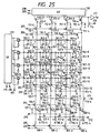
- Fig. 25 shows an 11th embodiment of the present invention, wherein components equivalent to those in Figs. 1 to 24 are represented by same numbers and will not be explained further.
- the present embodiment corresponding to a modification of the 10th embodiment, provides a two-dimensional array of the photoelectric conversion elements, wherein a block is formed by two pixels in the vertical direction and two pixels in the horizontal direction.
- Fig. 25 shows a 4 ⁇ 4 area sensor with 2 ⁇ 2 blocks, of which outputs are transferred through clamping circuits to the capacitances 107-1 to 107-4, while the pixel signals are transferred to the accumulation capacitances 112-1 to 112-4 driven by a vertical shift register 131.
- Time-sequential three-level pulses are applied from a terminal 101 to control the timing of resetting and accumulation of the pixels.
- the vertical shift register 131 receiving clock signals and timing signals from terminals 215, 216, releases pulses signals in succession, thereby scanning the pixels by turning on and off the switches.
- the photocarrier output signals accumulated in the bases of the NPN transistors 103-1 to 103-16, each having two emitters and constituting the pixels are transferred to the accumulation capacitances 112-1 to 112-4 and also, in a blockwise operation, to the buffer capacitances 107-1 to 107-4 through the coupling capacitances 105-1 to 105-4.
- the accumulation capacitances 112-1 to 112-4 are reset and the maximum block charges in the buffer capacitances 107-1 to 107-4 are transferred through the switch means 116-1 to 116-4 and output in succession from the terminal 211.
- the present embodiment can provide a wider image pickup area than in the 10th embodiment, by the addition of the photoelectric conversion pixels and the vertical scanning circuit, thereby enabling more precise detection with a higher sensitivity. Also the average value of the vertical pixels can be obtained without additional cycle time, by forming each vertical column of the present embodiment into a block and accumulating the average of the pixel signals in a buffer capacitance.
- the block signals are detected by the peak signals utilizing the NPN transistors 108-1, 108-2, but there may also be employed PNP transistors for detecting bottom signals. Also these two configurations may both be employed for achieving finer detection, according to the purpose of the photoelectric conversion device.
- the device of the present invention capable of releasing both an output signal obtained by pre-processing of the pixel signals and output signals of every pixels, can reduce the serial transfer time by such pre-processed signal output, in addition to the signal output in the conventional scanning operation. Also the presence or absence of the image can be speedily detected, without extension of the cycle time by the addition of the signal transfer time, even in case with a large number of pixels or in case of an area sensor with plural rows and columns.
- the fixed pattern noise can be effectively eliminated by the clamping circuits constituting the pre-processing circuits.
- the block formation of plural columns allows to reduce the amount of pixel signals and the cycle time, and the retain/transfer circuits and the output circuit can be used in common for the unprocessed signals.
- a high-speed and inexpensive solid-state image pickup device of a low power consumption without a major increase in the chip size.
Landscapes
- Engineering & Computer Science (AREA)
- Multimedia (AREA)
- Signal Processing (AREA)
- Transforming Light Signals Into Electric Signals (AREA)
- Solid State Image Pick-Up Elements (AREA)
Abstract
Description
- The present invention relates to a solid-state image pickup device.
- With the recent remarkable progress in the semiconductor technology, the solid-state image pickup device represented by the CCD has shown significant improvement in performance and has been applied in various products such as facsimile and scanner. In such trend, there are emerging stronger requirements for the solid-state image pickup device, not only for a higher performance such as a higher sensitivity or a higher resolving power, but also for drivability with a lower voltage. As a result, in the field of CCD, there have appeared products drivable with a 5 V power source and developments are being made to achieve drivability with a lower voltage.
- Also with a higher sensitivity, there is expected the application for a photodetector capable of detecting very weak light that has not been detectable and effecting signal processing on thus detected light.
- Also as a highly advanced ability of the solid-state image pickup device, there is required an ability to detect whether a certain light is present, and, upon detection of the light, to provide a detailed image output of the portion of such light.
- An example of the conventional bipolar solid-state image pickup device is shown in Figs. 1 and 2. Fig. 1 is an equivalent circuit diagram of a unit pixel, which is composed of an NPN
bipolar phototransistor 14, a pixel separating-resettingPMOS transistor 11, a basepotential control capacitor 13, a three-value pulse supply terminal PR, and a bias reset supply terminal VBR. - Fig. 2 shows a solid-state image pickup device consisting of a one-dimensional array of four bipolar photoelectric converting elements explained above, while a three-value pulse from a three-
pulse terminal 1 is in the LOW level state, a reset pulse is supplied from areset terminal 2 to render thePMOS transistors 11 conductive, whereby theNPN transistors 14 are reset. When the three-value pulse from the three-value pulse terminal 1 is shifted to the MIDDLE level state, the gate-source voltage VGS of the PMOS transistors 11-1 to 11-4 becomes lower than the threshold value Vth of the transistors, whereby these transistors are rendered non-conductive and a first resetting operation is completed. - Then, when the
reset terminal 33 is shifted to the high level state, the NMOS transistors 22 are rendered conductive and the emitters of theNPN transistors 14 are reset. Subsequently the three-value pulse terminal 1 is shifted to the high level state, whereby the bases of theNPN transistors 14 are shifted to the floating state through thecontrol capacitances 13, and, when the three-value terminal 1 is shifted to the middle level, there is initiated the accumulation of the photon charges by photoelectric conversion. Subsequently, after the lapse of a predetermined time, atransfer terminal 32 and the three-value pulse terminal 1 are shifted to the high level state, whereby the NMOS transistors 23 are rendered conductive, and the charges accumulated in the bases are transferred to transfer capacitances 24 by the application of a high-level pulse to thereset terminal 3. Then ahorizontal shift register 29, receiving astart pulse 30 and scanningpulses 31, releases scanning signals for rendering scanningNMOS transistors 25 conductive in succession, whereby the charges of the accumulating capacitances 24 are in succession transferred to anoutput line 42 and released to anoutput terminal 28 after amplification in anamplifier 41. After each signal output from the accumulating capacitance 24, a reset pulse is applied to thereset terminal 27 whereby the remaining charge on theoutput line 42 is dissipated to the ground through anNMOS transistor 26. The image of a line can be released through the above-explained operations, and the function as an area sensor can be achieved by repeating the above-explained operations in combination with a movement of the sensor. - As explained in the foregoing, the signals of the different pixels are once read into the transfer capacitances C24-1 to C24-4 and are then serially transferred to the output terminal by the function of the scanning circuit. The gain GT and the output voltage VO at the transferring operation are represented by:


- CT: capacity of transfer capacitances C24-1 to C24-4;
- CH: parasite capacitance including the capacity of the output line; and
- Vi: signal voltage retained in the transfer capacitances C24-1 to C24-4.
- The capacitance CH is composed of the drain capacitance and the gate overlapping capacitance of the scanning transistors 25-1 to 25-4 and the resetting
transistor 26, the input capacitance of the output amplifier and the parasite capacitance of the output wiring, and is heavily dependent on the number of pixels and the manufacturing process. It is in the order of several picofarads in case of several hundred pixels. On the other hand, CT is composed of the capacitances of the MOS device and of junctions, and is designed in the order of several picofarads in the actual integrated circuit. - Consequently the above-mentioned transfer gain is usually in the order of 0.3 to 0.4, and a larger gain leads to an increased cost because of an increased chip size. Consequently a gain of several times is applied in the subsequent stages if a larger signal value is required, but a sufficient gain is difficult to obtain in a low-voltage drive because of the limited input/output dynamic range.
- Also the image taking will not be required if the brightness of the image is low and does not reach the sensitivity of the pixels, but, if the image has a certain level of brightness, it is often required to obtain details of such lighted area. The image detection with a line sensor under such condition requires the scanning operation over the entire pixels, thus requiring a long time for the scanning operation with a large power consumption, and, if such brightness appears instantaneously, it is difficult to detect such instantaneous bright area.
- Also in the configuration shown in Fig. 2, the time for one cycle is principally used for pixel resetting, signal read-out and serial signal transfer, and the significant part is usually used for the serial transfer. This time becomes longer with the increase in the number of pixels, and, in case of an area sensor with plural lines, most of the cycle time is occupied by the signal transfer time. Consequently, in the application for a detector for detecting the presence or absence of an image at a high speed, it is an important issue how to reduce this time.
- The present inventors have disclosed, in the Japanese Patent Laid-open Application No. 6-268920, that this signal transfer time can be reduced by releasing a signal averaged over plural pixels. However, in the above-mentioned invention, though the signal averaging is easy in the horizontal direction of the area sensor, it can normally be made for 2 to 4 pixels in the vertical direction, as a larger averaging leads to an increase in the chip size. Consequently an inexpensive high-speed detector has been extremely difficult to realize with an area sensor.
- An object of the present invention is to provide a solid-state image pickup device provided with an array of plural blocks each of which is composed of two or more pixels, wherein the outputs of said block are connected in common, respectively through amplifier means.
- Another object of the present invention is to provide a solid-state image pickup device capable, for resolving the above-mentioned drawbacks, of outputting both an output signal obtained by pre-processing of the signals of the pixels and an output from each pixel, wherein the above-mentioned pre-processed output signal is output through output means for the signal of each pixel.
- Still other objects of the present invention, and the features thereof, will become fully apparent from the following description which is to be taken in conjunction with the attached drawings.
-
- Fig. 1 is a circuit diagram of a conventional photo-electric converting element;
- Fig. 2 is a circuit diagram of a conventional solid-state image pickup device;
- Fig. 3 is a schematic block diagram of an embodiment of the present invention;
- Fig. 4 is a circuit diagram of an embodiment of the present invention;
- Fig. 5 is a timing chart of an embodiment of the present invention;
- Fig. 6 is a circuit diagram of a photoelectric converting element in an embodiment of the present invention;
- Fig. 7 is a circuit diagram of an embodiment of the present invention;
- Fig. 8 is a timing chart of an embodiment of the present invention;
- Fig. 9 is a circuit diagram of an embodiment of the present invention;
- Fig. 10 is a timing chart of an embodiment of the present invention;
- Fig. 11 is a circuit diagram of an embodiment of the present invention;
- Fig. 12 is a block diagram showing the working principle of the present invention;
- Fig. 13 is a block diagram showing another working principle of the present invention;
- Fig. 14 is a circuit diagram of an embodiment of the present invention;
- Fig. 15 is a timing chart showing the functions of the embodiments shown in Figs. 14, 17 and 18;
- Fig. 16 is a timing chart showing other functions of the embodiments shown in Figs. 14, 17 and 18;
- Fig. 17 is a circuit diagram of an embodiment of the present invention;
- Fig. 18 is a circuit diagram of an embodiment of the present invention;
- Fig. 19 is a circuit diagram of a block-structured embodiment of the present invention;
- Fig. 20 is a circuit diagram of another block-structure embodiment of the present invention; and
- Figs. 21 to 25 are circuit diagrams of still other block-structured embodiments of the present invention.
- Now the function of the present invention will be schematically explained with reference to Fig. 3, in which there are shown
unit pixels 80 of a photoelectric converting element, pixel buffer means 81 for buffering pixel signals,function circuits 82 such as clamping circuits, and block buffer means 83 for buffering block signals. Signals from thepixels 80 are supplied respectively through the pixel buffers 81 and are wire-connected among every three pixels to provide block signals, which are subjected to a suitable signal processing in thefunction circuits 82 and wire-connected, after passing the block buffers 83, for all the blocks, whereby a signal representing all the blocks is output from anoutput terminal 84. - As all the above-mentioned operations are conducted collectively for all the pixels or all the blocks, there is only required an extremely short process time with a reduced power consumption. Also by constituting the block buffer means 83 with bipolar transistors and connecting the emitters thereof in common for all the blocks, the maximum value of the signals of all the blocks can be read out, without loss to the
output terminal 84. - In the foregoing there has been explained the image read-out in the block form, but a higher function of the solid-state image pickup device can be achieved, by reading out the signals of the pixels constituting the blocks as in the conventional solid-state image pickup device. More specifically, the image pickup device is featured by first photoelectric conversion means for reading out photoelectrically converted charge of each pixel and second photoelectric conversion means for reading out photoelectrically converted charge of each block consisting of plural pixels, wherein the outputs of the above-mentioned photoelectric conversion means are connected, through maximum output means, to a common line. This configuration will be explained in more details in the following embodiments.
- Fig. 4 illustrates a first embodiment of the present invention, composed of a one-dimensional array of four bipolar photoelectric conversion elements as employed in Fig. 1. In comparison with the configuration shown in Fig. 3, the
NPN transistor 14 serving as the bipolar photoelectric conversion element, thebase control capacitance 13 and the resettingPMOS transistor 11 correspond to thepixel 80. Also the emitter of theNPN transistor 14 corresponds to thepixel buffer 81, while the resettingNMOS transistor 12, thetransfer NMOS transistor 15 and the transfer capacitance 16 correspond to thefunction circuit 82, and the NPN transistor 17 and the constantcurrent source 18 correspond to theblock buffer 82. Also a block is constituted by the NPN transistors 14-1 and 14-2, while another block is constituted by the NPN transistors 14-3 and 14-4. - Now the function of the present embodiment will be explained with reference to a timing chart shown in Fig. 5.
- At first, at a time T0, a low level pulse is applied to the three-
value pulse terminal 1 to render the PMOS transistors 11-1 to 11-4 conductive, whereby the base areas of the photoelectric conversion elements are reset to a voltage given to the reset terminal 2 (first resetting). Then, at a time T1, the pulse to the three-value pulse terminal 1 is shifted to the middle level to shift the gate-source voltage VGS of the PMOS transistors 11-1 to 11-4 to a value not exceeding the transistor threshold voltage Vth, whereby the PMOS transistors are rendered non-conductive and the first resetting operation is completed. - Then, at a time T2, a high level pulse is applied to the
reset pulse terminal 3 to render the NMOS transistors 12-1, 12-2 conductive, whereby the emitters of thepixel NPN transistors 14 are reset to a reset voltage (which is the ground in the illustrated configuration). Subsequently, at a time T3, a high level pulse is applied to the three-value pulse terminal 1 to elevate the base potential of theNPN transistors 14 by the capacitative coupling through the base control capacitances 13-1 to 13-4 to generate a forward bias between the bases and the emitters, while the PMOS transistors 11-1 to 11-4 are maintained in the non-conductive state. As a result theNPN transistors 14 effect an emitter follower operation whereby the holes on the base areas in the floating state effect recombination and the base potentials are reset (second resetting). - After this resetting, at a time T4, the pulse to the three-
value pulse terminal 1 is lowered to the middle level, whereby the base potentials of the pixels are shifted to the negative side to generate an inverse bias between the bases and the emitters. At this point there is initiated the accumulation of the photoelectrically converted charges in the bases. - Then, at a time T5 after a predetermined accumulation time, a high level pulse is applied to the
transfer terminal 4 to render the NMOS transistors 15-1, 15-2 conductive, whereby the emitters of theNPN transistors 14 of all the pixels are connected to the capacitances 16-1, 16-2 and are at the same time reset to the ground level through the NMOS transistors 12-1, 12-2. At a time T6, the pulse to thereset pulse terminal 3 is shifted to the low level to render the NMOS transistors 12-1, 12-2 non-conductive. Then, at a time T7, a high level pulse is applied to the three-value pulse terminal 1 to shift the base potentials of all the pixels to the positive side through the capacitances 13-1 to 13-4, whereby a forward bias state is generated between the bases and emitters of the NPN transistors 14-1 to 14-4 of all the pixels. Thus the maximum voltages of the signals of thepixels pixels output line 2, the maximum voltage of the transfer capacitances 16-1, 16-2 is supplied to theoutput line 2. With the capacity CT of the transfer capacitances 16-1, 16-2, the parasite capacity CH of theoutput line 2, the current amplification factor hFE of the NPN transistors and the output voltages V1, V2 (V1 > V2) of the blocks read in the transfer capacitances 16-1, 16-2, the voltage V0 obtained on theoutput line 2 is given by:
- Then, at a time T8, the pulse to the
transfer terminal 4 is shifted to the low level state to terminate the readout operation, whereupon the transfer capacitances 16-1, 16-2 are maintained in the floating state and the output voltage becomes gradually lower. - The rate of decline of the output voltage is represented by:

current source 18 provided in the output stage, and CB is the base capacitance of the NPN transistors 17-1, 17-2, so that the output period can be made longer by selecting a small constant current IS. - The foregoing first embodiment employs NPN transistors for the block buffer means, but there may also be employed PNP transistors. In such case the bases are connected to the function circuits while the emitters are connected in common to a power source through a constant current source, and the collectors are grounded, and the output is obtained from the commonly connected emitters. In this configuration, in contrast to the foregoing configuration, the minimum potential of the blocks is output. Also by inverting the polarity of the foregoing embodiment, for example by employing a PNP transistor and an NMOS transistor for each pixel, the charge of a pixel having the minimum charge among all the pixels is output. Such configuration for detecting the minimum pixel charge is effective for instantaneous detection of a dark area, generated instantaneously in an extremely bright field.
- As explained in the foregoing, the configuration of the present invention can be advantageously utilized as a detector, as it enables high-speed readout of the pixel block signals without loss.
- Figs. 6 and 7 illustrate a second embodiment of the present invention, wherein components equivalent to those in Fig. 4 are represented by same numbers and will not be explained further. The present embodiment is an improvement on the first embodiment, and is capable of both the block signal readout of the first embodiment and the readout of the signals of all the pixels. The photoelectric conversion element employed in the present embodiment is composed, as shown in Fig. 6, of an
NPN transistor 21 with two emitters, aPMOS transistor 11 and capacitance means 13, wherein one of the two emitters is connected with those of other photoelectric conversion elements to constitute a pixel block, thereby outputting the maximum voltage among the pixels constituting the block. And another emitter is connected with a readout circuit as explained in conventional configuration. So that, it is a combination of the conventional configuration shown in Fig. 2 and the first embodiment shown in Fig. 4. - The function of the present embodiment will be briefly explained with reference to a timing chart shown in Fig. 8.
- At first, at a time T0, a low level pulse is applied to the three-
value pulse terminal 1 to effect first resetting of the pixels, and, at a time T1, a middle level pulse is applied to the three-value pulse terminal 1 to render thePMOS transistors 11 non-conductive. Then, at a time T2, high level pulses are applied to thereset terminal 3 and the terminal 33 to reset the two emitters of theNPN transistor 21 of each pixel to a reset potential (ground in the illustrated configuration). At a subsequent time T3, a high level pulse is applied to the three-value pulse terminal 1 to effect second resetting through theNMOS transistors 12, 22. At a time T4, the pulse to the three-value pulse terminal 1 is lowered to the middle level to terminate the resetting operation and to initiate the accumulation of the photoelectrically converted charges in the bases of theNPN transistors 21. - Then, at a time T5 after a predetermined accumulation time, high level pulses are applied to the
transfer terminals NMOS transistors 12, 22. Then, at a time T7, a high level pulse is applied to the three-value pulse terminal 1 to transfer the signals of the pixels respectively to the capacitances 24-1 to 24-4 and the highest voltages of thepixels pixels output line 2. Subsequently, at a time T8, the pulses at thetransfer terminals - Then, at a time T9, the pulse to the three-
value pulse terminal 1 is shifted down to the low level, and, at a time T10, a high level pulse is applied to thereset terminal 27 to reset theoutput line 42. Then, astart pulse 30 andscanning pulses 31 are supplied to thescanning circuit 29 respectively at times T11 and T12 whereby the signals of the pixels are time-sequentially read out to theoutput terminal 28, in synchronization with clock signals. - In the present embodiment, the signal of the blocks is read before the readout of the signal of each pixel, but the following drive is also possible for example in the application for a detector. The operations of the device can be significantly simplified by at first reading the block signal, then discriminating whether the block signal is larger (or smaller) than a predetermined value, and, if larger (or smaller), reading the signals of every pixels, but, if smaller (or larger), terminating the each signal readout from the pixels because the signal level of the pixels is too low. In this manner it is possible to reduce the process time and to significantly reduce the power consumption.
- Fig. 9 shows a third embodiment of the present invention, wherein components equivalent to those in Fig. 4 are represented by same numbers and will not be explained further. In addition to the second embodiment, the present embodiment is provided, serially to the vertical output lines, with capacitance means 38-1 to 38-4 and capacitance means 36-1, 36-2 to effect clamping operations for the signals, thereby eliminating FPN (fixed pattern noise) and random noises, and also eliminating external light components other than the reflected light, in case of irradiating an object with light from a light source such as an LED and taking the reflected light. Such functions will be briefly explained in the following with reference to a timing chart shown in Fig. 10.
- At first, in a period from a time T0 to T7, there are executed first and second resetting of the pixels, a first accumulating operation and a signal readout operation. Then at the time T7 immediately before the end of the readout operation, pulses at the
reset terminals reset terminals output terminal 5, and, on the other hand, thescanning circuit 29 is driven after a time T19 to time-sequentially output the signals of every pixels from theoutput terminal 28. - As an output corresponding to the dark signal can be obtained by selecting an extremely short accumulation time for the first accumulation, so that FPN (fixed pattern noise), which is a drawback of the amplifying solid-state image pickup device, can be eliminated by obtaining the difference between the above-mentioned output and the second output. Also by selecting a same accumulation time for the first and second accumulations and irradiating the object with the light from the light source such as an LED during the second accumulation time, the reflected image of the object can be precisely read out even in a bright indoor situation, and such ability is suitable particularly for a detector.
- Also in the present embodiment, it is possible to reduce the signal readout time and the power consumption by detecting the pixel block signal and reading the individual pixel signals only when necessary, as already explained in the second embodiment. Also in the present embodiment, the block signals and the individual pixel signals are also output through the clamping circuits, but such clamping circuits may naturally be dispensed with.
- Fig. 11 shows a fourth embodiment of the present invention, wherein components equivalent to those in Fig. 4 are represented by same numbers and will not be explained further. In comparison with the third embodiment, the present embodiment provides an area sensor consisting of a two-dimensional array of the photoelectric conversion elements.
- In Fig. 11, each block is composed of two pixels in the vertical direction and two pixels in the horizontal direction, and the outputs of the blocks are transferred to transfer capacitances 24-1 to 24-4, while the pixel signals are driven by the output of a vertical shift register. The present embodiment, providing a larger image pickup area than in the third embodiment, can achieve more precise detecting operation.
- Referring to Fig. 11, in response to a
start pulse 50 andvertical scanning pulses 51, a verticalscanning shift register 43 sends horizontal scanning pulses in succession to horizontal lines, thereby controlling switches 44-1 to 44-4 including inverters. The three-value pulse entered from the three-value pulse terminal 1 is turned on and off by the switches 44 to at first activate the pixels of the 1st and 2nd horizontal scanning lines, composed of the NPN transistors 21-11 to 21-14 and 21-21 to 21-24, whereby the signals of these pixels are transferred to the transfer capacitances 24-1 to 24-4 and are output in succession to theoutput terminal 28 through theoutput line 42. On the other hand, in the block unit, the charges obtained from the NPN transistors 21-11, 21-12, 21-21 and 21-22 are transferred to a coupling capacitance 36-2 while those obtained from the NPN transistors 21-13, 21-14, 21-23 and 21-24 are transferred to a coupling capacitance 36-4 and then transferred to transfer capacitances 16-2, 16-4, whereby a voltage corresponding to the maximum charge in the blocks are obtained at theoutput terminal 5. - In the present embodiment, each block is composed of 2 × 2 pixels, but there may employed a larger number of pixels for constituting a block. In comparison with conventional readout of each pixel, a larger number of pixels improves the S/N ratio of the output at the
output terminal 5 and enables image readout at a higher speed, thereby enabling image pickup with a higher precision, in combination with the readout of the pixel signals. - In the foregoing embodiments, the signal of each block is detected with a peak signal, obtained from NPN transistors, but it is also possible to detect a bottom signal with PNP transistors, and both may be employed in combination for achieving finer detection.
- The foregoing embodiments have all been constructed with bipolar photoelectric conversion elements, but similar effects can be obtained also with XY-addressable photoelectric conversion elements such as CMD, AMI or FGA.
- As explained in the foregoing, the 1st to 4th embodiments have the following technological advantages.
- Enabling high-speed readout of the pixel block signal without loss, are advantageously applicable to detectors. It is also possible to significantly simplify the operation, in certain applications such as for detector, to at first read out the block signal, then to discriminate whether such block signal is larger (or smaller) than a predetermined value, and, if it is larger (or smaller), to read out the pixel signals in succession, but, if it is smaller (or larger), to terminate the signal readout as the level of the pixel signals is too low. In this manner it is rendered possible to reduce the process time and the power consumption. Also, in the utilization of the block signal, there can be obtained an output corresponding to a dark area by selecting a very short first accumulation time, and the FPN (fixed pattern noise), which is a drawback of the amplifying solid-state image pickup device, can be eliminated by obtaining the difference between the above-mentioned output and the second output. Also by selecting a same accumulation time for the first and second accumulating operations and irradiating the object with the light from a light source such as an LED in the course of the second accumulating time, the reflected image of the object can be read out in highly precise manner even in a bright indoor situation. Such function can be advantageously utilized particularly in a detector.
- In the following the function and effect of a 5th embodiment will be briefly explained with reference to Fig. 12, wherein shown are unit pixels 51-1 to 51-8; transfer means 50-1 to 50-8 for retaining the pixel signals of the unit pixels 51-1 to 51-8 in accumulating capacitances and then serially outputting the pixel signals to an
output line 55; pre-process means 52-1 to 52-8 connected to the unit pixels 51-1 to 51-8 for effecting a pre-process; buffer means 53-1 to 53-8 for buffering the signals from the pro-process means; and switching means 54-1 to 54-8 connecting the transfer means 50-1 to 50-8 with the buffer means 53-1 to 53-8. The buffer means 53-1 to 53-8 may be dispensed with if unnecessary. - In the present embodiment, the signals of the unit pixels 51-1 to 51-8 are transferred to the transfer means 50-1 to 50-8 for retaining the signal of each pixel, and are output to a terminal 57 through an
output line 55 and anoutput circuit 56. Also they are subjected to a suitable pre-processing in the pre-process means 52-1 to 52-8, then transferred to the transfer means 50-1 to 50-8 through the buffer means 53-1 to 53-8, and released to the terminal 57. Naturally the unprocessed signals and the pre-processed signals have to be released in different periods. It is also possible to form the unprocessed signals and the pre-processed signals into blocks in the transfer means 50-1 to 50-8 and to output these signals by serial transfer after mixing thereof. - The transfer means 50-1 to 50-8 can be realized, for example, by the accumulating capacitances 24-1 to 24-4, the switch means 25-1 to 25-4 and the
scanning circuit 29 shown in Fig. 2, and the pre-process circuit can be composed of an FPN (fixed pattern noise) elimination circuit utilizing a clamping circuit to be explained later. - Also in a configuration shown in Fig. 13, in which components same as those in Fig. 12 are represented by same numbers, the signals pro-processed in the pre-process means 52-1 to 52-8 are buffered by the buffer means 53-1 to 53-8, and plural columns are formed into a block, of which signal is transferred to retain/transfer means. This configuration allows to reduce the amount of pixel signals and to significantly reduce the cycle time, and the retain/transfer circuits and the output circuit can be used in common for the unprocessed signals, so that a major increase in the chip size is not required. It is therefore possible to provide a high-speed and inexpensive solid-state image pickup device of a low power consumption by normally reading out the block signal and effecting the detecting operation based on this block signal, and reading out the signals of every pixels only when necessary. Such function will be explained in detail in the following embodiment.
- Fig. 14 shows a 6th embodiment of the present invention, employing four bipolar photoelectric conversion elements shown in Fig. 1, arranged in a linear array. In Fig. 14, components equivalent to those in Fig. 2 are represented by same numbers. In addition, the present embodiment is provided, as explained in the foregoing embodiment shown in Fig. 12, with pre-processing means composed of coupling capacitances 105-1 to 105-4 and NMOS transistors 106-1 to 106-4; buffer means composed of buffer capacitances 107-1 to 107-4 and NMOS transistors 109-1 to 109-4; and switch means composed of NMOS transistors 116-1 to 116-4.
- In the following, the function of the present embodiment will be explained with reference to a timing chart shown in Fig. 15. At first high level pulses are supplied to
terminals - At a time T0, a low level pulse is supplied to a terminal 201 to render the PMOS transistors 101-1 to 101-4 conductive whereby the base areas of the photoelectric conversion elements are reset to a voltage given to a terminal 202 (first resetting). Then the pulse to the terminal 201 is shifted to the middle level to reduce the gate-source voltage VGS of the PMOS transistors 101-1 to 101-4 to a value not exceeding the threshold value Vth thereof, whereby these PMOS transistors are rendered non-conductive and the first resetting operation is completed.
- Then, at a time T1, a high level pulse is applied to a terminal 206 to render the NMOS transistors 110-1 to 110-4 conductive, whereby the emitter of the NPN transistors of the pixels is reset to a reset potential (ground in the illustrated configuration).
- Then, at a time T2, a high level pulse is applied to the terminal 201 to elevate the base potential of the NPN transistors by the capacitative coupling through the capacitances 102-1 to 102-4 thereby generating a forward bias between the bases and the emitters, while the PMOS transistors 101-1 to 101-4 are retained in the non-conductive state, whereby the NPN transistors 103-1 to 103-4 effect an emitter follower operation. As a result the holes on the base areas in the floating state effect photorecombination and the base potential is reset (second resetting operation).
- At a time T3 after this resetting operation, the pulse to the terminal 201 is shifted down to the middle level to shift the base potentials of the pixels to the negative side, whereby an inverse bias state is generated between the bases and the emitters and an accumulating operation is thereby initiated (first accumulating operation).
- At a time T4 after a predetermined accumulation time, the pulse to the terminal 206 is shifted down to the low level state to render the NMOS transistors 110-1 to 110-4 non-conductive, whereby the emitters of the pixel transistors 103-1 to 103-4 and the capacitances 112-1 to 112-4 are shifted to a floating state.
- Then, at a time T5, a high level pulse is applied to a terminal 201 to shift the base potentials of the pixels to the positive side through the capacitances 102-1 to 102-4, thereby generating a forward bias between the bases and emitters of the NPN transistors 103-1 to 103-4 of the pixels. Consequently the signals obtained by photoelectric conversion in the respective pixels and accumulated in the base areas are respectively transferred to the accumulation capacitances 112-1 to 112-4 and the coupling capacitances 105-1 to 105-4.
- Then, at a time T6 immediately before the completion of the readout operation, the pulse to the terminal 205 is shifted down to render the NMOS transistors 109-1 to 109-4 non-conductive.
- Subsequently, at a time T7, the pulse to the terminal 201 is shifted down to turn off the NPN transistors 103-1 to 103-4 through the capacitances 102-1 to 102-4 whereby the readout operation is terminated.
- Then, at a time T8, a high level pulse is again applied to the terminal 206 to reset the emitters of the pixel NPN transistors 103-1 to 103-4 to the reset potential (ground in the illustrated configuration), whereby the voltages of the buffer capacitances 107-1 to 107-4 are shifted to the negative side by the capacitative coupling of the coupling capacitances 105-1 to 105-4. There stands the following relationship between the signal VR transferred to the coupling capacitances 105-1 to 105-4 and the signal VR' after the above-mentioned negative shifting:

- CC: capacity of the coupling capacitances 105-1 to 105-4;
- CT: capacity of the buffer capacitances 107-1 to 107-4; and
- CS: parasite capacity including the gate capcitance of the NMOS transistors 106-1 to 106-4.
- Then, in a period from a time T9 to T14, there are conducted operations similar to those in the period from T0 to T4, except that the NMOS transistors 109-1 to 109-4 are turned off, whereby the photoelectric conversion elements are reset and the photocarriers are accumulated (second accumulating operation). Then, at a time T14, there is executed a signal readout operation to provide signal voltages, added to the voltages obtained according to the equation (4). As a result, difference signals between the photoelectric conversion signals obtained in the first accumulation time and those obtained in the second accumulation time are retained in the buffer capacitances 107-1 to 107-4.
- Then, at a time T16, a high level pulse is applied to the terminal 206 to reset the accumulation capacitances 112-1 to 112-4 again, and, at a time T17, a high level pulse is applied to a terminal 213 to render the NMOS transistors 116-1 to 116-4 conductive, whereby the signals in the buffer capacitances 107-1 to 107-4 are transferred to the accumulation capacitances 112-1 to 112-4.
- Then at a time T18, the
terminals - Then, starting from a time T19, a
scanning circuit 130 is activated with the resetting of anoutput line 140, thereby serially transferring the signals of the accumulation capacitances 112-1 to 112-4 to anoutput terminal 211, and the operations of a series are thus completed. It is also possible to eliminate the FPN (fixed pattern noise) in these operations, by selecting a very short first accumulation time to obtain a signal corresponding to the dark area, and calculating the difference of the above-mentioned signal and the signal obtained in the second accumulation. - Also by selecting a same accumulation time in the first and second accumulating operations and irradiating the object with the light from a light source such as an LED in the course of the second accumulation time, there can be eliminated the component of the external light even in an outdoor situation, whereby an exact object detection can be achieved.
- In the foregoing there has been explained the output of the pre-processed signals, but the unprocessed signals may also be obtained according to a timing chart shown in Fig. 16. The operations shown in Fig. 16, corresponding to a partial modification of those in Fig. 15, effect two accumulations while maintaining the terminal 213 at the low level state even at the time T17 to finally provide the signals obtained in the second accumulation, so that the period from T0 to T9 may be totally dispensed with.
- In Fig. 16, the terminal 213 is always maintained at the low level state, whereby the NMOS transistors 115-1 to 115-4 are always in the non-conductive state. Consequently the calculation in the clamping circuits does not at all affect the accumulation capacitances 112-1 to 112-4, so that, in the readout operation, the pixel signals are directly read out to the accumulation capacitances 112-1 to 112-4 as in the conventional configuration, and they are not reset but are serially output by the
scanning circuit 130. Such direct readout of the sensor signals is effective for improving the detecting sensitivity, for example in case of detecting an object of relatively low luminance, as in an indoor situation, since the clamping process reduces the output as represented by the equation (4). - In the configuration shown in Fig. 14, the pre-processing circuit is composed of a difference calculating circuit utilizing a clamping circuit, but it is also possible, as shown in Fig. 17, to effect signal averaging among the adjacent pixels as the pre-processing, by providing retaining capacitances 118-1 to 118-8, grouped by two and connected respectively to the vertical output lines through switch means 117-1 to 117-4, also providing switch means for connecting the retaining capacitances between the adjacent pixels and connecting the outputs of these switch means to the emitters of the NPN transistors 103-1 to 103-4 through transfer switches 116-1 to 116-4.
- It is also possible to serially read the signals of different accumulation periods, as shown in Fig. 18, into the capacitances 112-1 to 112-4 and 135-1 to 135-4. Specifically, at first, the signals of an accumulation period is read into the capacitances 112-1 to 112-4 and the signals of another accumulation period is read into the capacitances 135-1 to 135-4. After the signals retained in the capacitances 112-1 to 112-4 are serially read out to capacitances 112-1 to 112-4 and output to the
line 42 in the same manner. Also by arranging the pixels in a two-dimensional array in the present embodiment, it is rendered possible to retain the maximum signals of the pixels in the respective vertical columns in the capacitances 135-1 to 135-4 and to output these signals at a timing different from that of output of the pixel signals. - Also the pre-processing circuit may be composed of a calculation circuit utilizing an operational amplifier.
- Fig. 19 shows a 7th embodiment of the present invention, wherein components equivalent to those in Figs. 1 to 18 are represented by same numbers and will not be explained further. The photoelectric conversion element employed in the present embodiment is similar to that shown in Fig. 6. One of the two emitters is connected in common among the pixels constituting a pixel block, whereby the maximum voltage of the pixels constituting the block is accumulated in either of the buffer capacitances 107-1, 107-2. Such maximum voltages are transferred to the accumulation capacitances 112-1, 112-3 and output from the terminal 211 through the function of the
scanning circuit 130. - The driving method of the present embodiment is similar to that explained in Fig. 15 or 16, whereby the terminal 203 is driven simultaneously with the terminal 206 to effect resetting and accumulation.
Consequently, the output of each block representing the highest output level within the block, is read out, and the detecting operation is executed by this output in the ordinary state. It is also possible, based on the result of such detecting operation, to read out the signals of every pixels if necessary. As there is obtained the output of the pixel of highest output level among the plural pixels within the block, there can be achieved an improvement in the detecting precision and a significant reduction in the amount of signals, leading to a reduced cycle time and a reduction in the power consumption. - Fig. 20 shows an 8th embodiment of the present invention, wherein components equivalent to those in Figs. 1 to 19 are represented by same numbers and will not be explained further. The present embodiment, corresponding to an improvement on the 7th embodiment, is provided the buffer capacitances 107-1, 107-2 at the output of the clamping circuits, with NPN transistors 108-1, 108-2 of which emitters are connected in common and further connected to a constant
current source 115 and anoutput terminal 212. - In the present embodiment, after the clamping operation, the maximum value of the signals transferred to the buffer capacitances 107-1, 107-2 is immediately output to the terminal 212 without the function of the
scanning circuit 130, so that the cycle time and the power consumption can be further reduced in comparison with the 7th embodiment. Instead of the NPN transistors employed in the present embodiment, there may be employed PNP transistors in emitter follower circuits to provide the minimum value of the block signals at the terminal 212. Consequently the present embodiment can achieve a function of detecting whether the signal is higher (or lower) than a predetermined level and then reading out the signals of the blocks or pixels based on the result of such detection according to the need so that the photoelectrically converted output can be obtained, matching the intention of photoelectric conversion. - Also in Fig. 20, the buffer capacitances 107-1, 107-2 are reset to the ground potential by the NMOS transistors 109-1 and 109-2, but it is more effective for reading out small output voltages, as shown in Fig. 21, by providing a reset
power source terminal 231 in order to generate a sufficient forward bias voltage between the bases and the emitters of the NPN transistors 108-1, 108-2. - Also in the configuration shown in Fig. 20, the signals of the buffer capacitances 107-1, 107-2 are read out by the emitter follower circuits utilizing the constant
current source 115, so that the signal voltage of the buffer capacitance declines, during a readout time TR, by:current source 115, and CB is the capacity of the buffer capacitance. Such loss in the signal voltage can be reduced to:
- Fig. 23 shows a 9th embodiment of the present invention, wherein components equivalent to those in Figs. 1 to 22 are represented by same numbers and will not be explained further. In the 6th to 8th embodiments, the buffer capacitances 107-1 to 107-4 and the accumulation capacitances 112-1 to 112-4 are connected through the switches 116-1 to 116-4, so that the transfer gain, represented by:

- CT: capacity of the buffer capacitances 107-1 to 107-4;
- CT2: capacity of the accumulation capacitances 112-1 to 112-4;
- CS2: parasite capacity between the buffer capacitances 107-1 to 107-4 including the gate capacitances of the NMOS transistors 116-1 to 116-4 and the accumulation capacitances 112-1 to 112-4.
- In the present embodiment, the buffer capacitances 107-1, 107-2 are provided with emitter follower circuits utilizing NPN transistors 108-1, 108-2 and the outputs thereof are connected to the accumulation capacitances 112-1, 112-3 through the switches 116-1, 116-2. Consequently, as regardless of the capacity of the parasite capacitance CS2 the signals can be transferred to the accumulation capacitances 112-1 to 112-4 almost without loss. Such configuration is effective in case the signals from the sensors are small.
- Fig. 24 shows a 10th embodiment of the present invention, wherein components equivalent to those in Figs. 1 to 23 are represented by same numbers and will not be explained further. The present embodiment corresponds to a combination of the 8th and 9th embodiments, wherein the emitters of the NPN transistors 108-1, 108-2 of the 9th embodiment are connected by an
NMOS transistor 117 to provide the maximum block output from the terminal 212. As explained in the 8th embodiment, the carriers of the buffer capacitance 107-2 can be immediately obtained as the maximum block output, and the carriers of the buffer capacitance 108-1 can also be obtained by the subsequent application of a high level pulse to the terminal 214. In this manner the block outputs can be read out without loss. - Fig. 25 shows an 11th embodiment of the present invention, wherein components equivalent to those in Figs. 1 to 24 are represented by same numbers and will not be explained further. The present embodiment, corresponding to a modification of the 10th embodiment, provides a two-dimensional array of the photoelectric conversion elements, wherein a block is formed by two pixels in the vertical direction and two pixels in the horizontal direction. Fig. 25 shows a 4 × 4 area sensor with 2 × 2 blocks, of which outputs are transferred through clamping circuits to the capacitances 107-1 to 107-4, while the pixel signals are transferred to the accumulation capacitances 112-1 to 112-4 driven by a
vertical shift register 131. Time-sequential three-level pulses are applied from a terminal 101 to control the timing of resetting and accumulation of the pixels. Thevertical shift register 131, receiving clock signals and timing signals fromterminals - Thus, in response to a high level pulse to the terminal 206, the accumulation capacitances 112-1 to 112-4 are reset and the maximum block charges in the buffer capacitances 107-1 to 107-4 are transferred through the switch means 116-1 to 116-4 and output in succession from the terminal 211.
- Also in response to a pulse applied to the terminal 214, there can be obtained, from the terminal 212, an output corresponding to the maximum among all the 16 pixels.
- The present embodiment can provide a wider image pickup area than in the 10th embodiment, by the addition of the photoelectric conversion pixels and the vertical scanning circuit, thereby enabling more precise detection with a higher sensitivity. Also the average value of the vertical pixels can be obtained without additional cycle time, by forming each vertical column of the present embodiment into a block and accumulating the average of the pixel signals in a buffer capacitance.
- In the foregoing embodiment, the block signals are detected by the peak signals utilizing the NPN transistors 108-1, 108-2, but there may also be employed PNP transistors for detecting bottom signals. Also these two configurations may both be employed for achieving finer detection, according to the purpose of the photoelectric conversion device.
- Also the foregoing embodiments have been constructed with the bipolar photoelectric conversion elements, but similar effects can also be obtained with other photoelectric conversion elements such as CMOS, CMD, AMI or FGA.
- As explained in the foregoing, the device of the present invention, capable of releasing both an output signal obtained by pre-processing of the pixel signals and output signals of every pixels, can reduce the serial transfer time by such pre-processed signal output, in addition to the signal output in the conventional scanning operation. Also the presence or absence of the image can be speedily detected, without extension of the cycle time by the addition of the signal transfer time, even in case with a large number of pixels or in case of an area sensor with plural rows and columns.
- Also the fixed pattern noise can be effectively eliminated by the clamping circuits constituting the pre-processing circuits.
- Also the block formation of plural columns allows to reduce the amount of pixel signals and the cycle time, and the retain/transfer circuits and the output circuit can be used in common for the unprocessed signals. Thus there can be provided a high-speed and inexpensive solid-state image pickup device of a low power consumption without a major increase in the chip size.
Claims (35)
- A solid-state image pickup device provided with an array of plural blocks, each comprising at least two pixels, wherein the output signals of said blocks are connected in common respectively through block buffer means, thereby outputting the maximum or minimum value of said pixels.
- A solid-state image pickup device according to claim 1, wherein said block buffer means has an input at the base of a self-biased transistor and has an output in an emitter follower circuit.
- A solid-state image pickup device according to claim 1, wherein said block buffer means comprises an NPN transistor.
- A solid-state image pickup device according to claim 1, wherein said block buffer means comprises a PNP transistor.
- A solid-state image pickup device comprising first photoelectric conversion means for reading out the photoelectric conversion charge from each pixel and second photoelectric conversion means for reading out the photoelectric conversion charge from each block comprising a plurality of said pixels, wherein the outputs of said second photoelectric conversion means are connected to a common line through maximum output means.
- A solid-state image pickup device according to claim 5, wherein said maximum output means has, for each block, an input at the base of a transistor and an output of an emitter follower circuit.
- A solid-state image pickup device according to claim 5, wherein said pixel comprises a transistor having at least two emitters.
- A solid-state image pickup device provided with plural photoelectric conversion pixels for converting optical signals into electrical signals, and transfer means for outputting the electrical signals from said photoelectric conversion pixels, comprising:pre-process means for pre-processing the electrical signals from said photoelectric conversion pixels;buffer means for transferring the output of said pre-process means to a next stage; andswitch means for transferring the output of said buffer means to said transfer means.
- A solid-state image pickup device according to claim 8, wherein said pre-process means comprises a clamping circuit.
- A solid-state image pickup device according to claim 8, wherein said buffer means includes a buffer capacitance.
- A solid-state image pickup device according to claim 8, wherein said switch means is turned on after an electrical signal accumulated in said transfer means is dissipated.
- A solid-state image pickup device according to claim 8, wherein said switch means is turned on for a block of a plurality of said buffer means.
- A solid-state image pickup device provided with photoelectric conversion means including a photoelectric conversion element for converting an optical signal into an electrical signal, transfer means with an accumulation capacitance for transferring said electrical signal, and scanning means for outputting the charge of said accumulation capacitance to an output line, comprising:pre-process means provided with a coupling capacitance for temporarily storing said electrical signal;buffer means provided with a buffer capacitance for transferring the charge of said coupling capacitance; andswitch means for transferring the charge of said buffer capacitance to said accumulation capacitance.
- A solid-state image pickup device according to claim 13, wherein said photoelectric conversion element includes an NPN transistor having two emitters, one of which is connected to an end of said switch means and to said transfer means, while the other of which is connected to said process means.
- A solid-state image pickup device according to claim 13, further comprising buffer output means for outputting the charge of said buffer capacitance.
- A solid-state image pickup device according to claim 15, wherein said buffer output means is adapted to the charge of said buffer capacitance obtained in a block composed of plural photoelectric conversion pixels, in superposed manner for plural blocks.
- A signal processing device provided with a process circuit for effecting plural processes in parallel manner on a signal output from a signal source, wherein at least one of the outputs of said process circuit is time-sequentially output from a common output circuit.
- A signal processing device according to claim 17, wherein said signal source is a solid-state image pickup device.
- An image pickup method for a solid-state image pickup device provided with photoelectric conversion means including a photoelectric conversion element for converting an optical signal into an electrical signal, transfer means provided with an accumulation capacitance for transferring said electrical signal, and scanning means for outputting the charge of said accumulation capacitance to an output line, comprising steps of:accumulating the charge of said electrical signal temporarily in a coupling capacitance;transferring the charge of said coupling capacitance to a buffer capacitance;dissipating the charge of said accumulation capacitance; andtransferring the charge of said buffer capacitance to said accumulation capacitance.
- Photoelectric conversion apparatus comprising a plurality of blocks, each block comprising a plurality of pixels, and means to read from a block a signal derived from the outputs of the plurality of pixels in the block (e.g. the maximum of the outputs of the pixels of the block).
- Apparatus according to claim 20 comprising a common output line for a plurality of the blocks.
- Apparatus according to claim 21 comprising means to read a signal from the common output line derived from the outputs of the plurality of blocks (e.g. the maximum of the outputs of the blocks).
- Apparatus according to claim 20 or claim 21 comprising means to read respective signals from respective blocks in turn.
- Apparatus according to any one of claims 20 to 23 comprising means to read respective signals from individual pixels to an output.
- Apparatus according to claim 24 in which the signals from the blocks are read to a different output from the signals from individual pixels.
- Apparatus according to claim 24 in which the signals from the blocks are read to the same output as the signals from individual pixels.
- Photoelectric conversion apparatus comprising a plurality of pixels, pre-process means for pre-processing signals from the pixels, means to read signals from the pixels to the pre-process means, and means to read signals from the pixels for output.
- Apparatus according to claim 27 in which the signals read for output are combined with the signals read to the pre-process means to provide combined signals to an output.
- Apparatus according to claim 27 in which the signals read for output are output without pre-processing, and pre-processed signals are output from the pre-processing means.
- Apparatus according to claim 29 in which the pre-processed signals are output from a different output from the signals output without pre-processing.
- Apparatus according to claim 29 in which the pre-processed signals are output from the same output as the signals output without pre-processing.
- Apparatus according to any one of claims 27 to 31 in which the pre-process means pre-processes signals from individual pixels separately.
- Apparatus according to any one of claims 27 to 31 in which the pre-process means pre-processes signals from a plurality of pixels in combination.
- Apparatus according to any one of claims 27 to 33 in which the pre-process means performs subtraction processing on the signals.
- Apparatus according to any one of claims 27 to 33 in which the pre-process means performs averaging processing on the signals.
Applications Claiming Priority (4)
| Application Number | Priority Date | Filing Date | Title |
|---|---|---|---|
| JP7015342A JP3017036B2 (en) | 1995-02-01 | 1995-02-01 | Solid-state imaging device |
| JO1534295 | 1995-02-01 | ||
| JP7167407A JP2907268B2 (en) | 1995-07-03 | 1995-07-03 | Signal processing device, solid-state imaging device, and imaging method of the device |
| JO16740795 | 1995-07-03 |
Publications (3)
| Publication Number | Publication Date |
|---|---|
| EP0725535A2 true EP0725535A2 (en) | 1996-08-07 |
| EP0725535A3 EP0725535A3 (en) | 1997-11-19 |
| EP0725535B1 EP0725535B1 (en) | 2003-04-23 |
Family
ID=26351462
Family Applications (1)
| Application Number | Title | Priority Date | Filing Date |
|---|---|---|---|
| EP96300696A Expired - Lifetime EP0725535B1 (en) | 1995-02-01 | 1996-01-31 | Solid-state image pickup device and method of operating the same |
Country Status (3)
| Country | Link |
|---|---|
| US (1) | US6657664B2 (en) |
| EP (1) | EP0725535B1 (en) |
| DE (1) | DE69627559T2 (en) |
Cited By (2)
| Publication number | Priority date | Publication date | Assignee | Title |
|---|---|---|---|---|
| WO1999066709A2 (en) * | 1998-06-17 | 1999-12-23 | Foveon, Inc. | Reducing striped noise in cmos image sensors |
| EP0977427A3 (en) * | 1998-07-30 | 2007-05-02 | Canon Kabushiki Kaisha | Signal processing apparatus |
Families Citing this family (9)
| Publication number | Priority date | Publication date | Assignee | Title |
|---|---|---|---|---|
| JP4006075B2 (en) * | 1998-01-30 | 2007-11-14 | キヤノン株式会社 | CMOS sensor and imaging system |
| US6850278B1 (en) * | 1998-11-27 | 2005-02-01 | Canon Kabushiki Kaisha | Solid-state image pickup apparatus |
| US6693670B1 (en) * | 1999-07-29 | 2004-02-17 | Vision - Sciences, Inc. | Multi-photodetector unit cell |
| JP3710334B2 (en) * | 1999-08-04 | 2005-10-26 | キヤノン株式会社 | Imaging device |
| JP3658278B2 (en) * | 2000-05-16 | 2005-06-08 | キヤノン株式会社 | Solid-state imaging device and solid-state imaging system using the same |
| US7336309B2 (en) * | 2000-07-05 | 2008-02-26 | Vision-Sciences Inc. | Dynamic range compression method |
| JP4031706B2 (en) * | 2000-11-27 | 2008-01-09 | ビジョン−サイエンシズ・インコーポレイテッド | CMOS image sensor with programmable resolution |
| US7224388B2 (en) * | 2003-05-08 | 2007-05-29 | Micron Technology, Inc. | Wide dynamic range active pixel with knee response |
| JP5274420B2 (en) * | 2009-09-24 | 2013-08-28 | キヤノン株式会社 | Photoelectric conversion device and imaging system |
Citations (5)
| Publication number | Priority date | Publication date | Assignee | Title |
|---|---|---|---|---|
| EP0275217A2 (en) * | 1987-01-16 | 1988-07-20 | Canon Kabushiki Kaisha | Photoelectric converting apparatus |
| US5335008A (en) * | 1991-03-08 | 1994-08-02 | Sony Corporation | Imager which has a load transistor connected to each vertical signal line and wherein each load transistor comprises two field transistors connected in series |
| EP0616464A2 (en) * | 1993-03-15 | 1994-09-21 | Canon Kabushiki Kaisha | Signal processor |
| EP0627847A2 (en) * | 1993-05-28 | 1994-12-07 | Canon Kabushiki Kaisha | Photoelectric conversion device |
| EP0630152A2 (en) * | 1993-06-18 | 1994-12-21 | Canon Kabushiki Kaisha | Photo-electric converter |
Family Cites Families (10)
| Publication number | Priority date | Publication date | Assignee | Title |
|---|---|---|---|---|
| JPS56116374A (en) * | 1980-02-20 | 1981-09-12 | Sony Corp | Charge detection circuit |
| EP0272152B1 (en) * | 1986-12-18 | 1994-08-03 | Canon Kabushiki Kaisha | Signal reading out circuit |
| US5262870A (en) | 1989-02-10 | 1993-11-16 | Canon Kabushiki Kaisha | Image sensor in which reading and resetting are simultaneously performed |
| US5162912A (en) | 1989-04-10 | 1992-11-10 | Canon Kabushiki Kaisha | Photoelectric conversion apparatus eliminating noise in an output signal |
| DE69131368T2 (en) | 1990-04-23 | 1999-11-18 | Canon K.K., Tokio/Tokyo | Photoelectric conversion device |
| US5134489A (en) * | 1990-12-28 | 1992-07-28 | David Sarnoff Research Center, Inc. | X-Y addressable solid state imager for low noise operation |
| JPH04313268A (en) * | 1991-04-10 | 1992-11-05 | Sony Corp | Solid-state image pickup device |
| JP3437208B2 (en) | 1993-03-15 | 2003-08-18 | キヤノン株式会社 | Signal processing device |
| JP3287056B2 (en) * | 1993-03-24 | 2002-05-27 | ソニー株式会社 | Solid-state imaging device |
| US5452004A (en) * | 1993-06-17 | 1995-09-19 | Litton Systems, Inc. | Focal plane array imaging device with random access architecture |
-
1996
- 1996-01-31 EP EP96300696A patent/EP0725535B1/en not_active Expired - Lifetime
- 1996-01-31 DE DE69627559T patent/DE69627559T2/en not_active Expired - Fee Related
- 1996-02-01 US US08/595,173 patent/US6657664B2/en not_active Expired - Fee Related
Patent Citations (5)
| Publication number | Priority date | Publication date | Assignee | Title |
|---|---|---|---|---|
| EP0275217A2 (en) * | 1987-01-16 | 1988-07-20 | Canon Kabushiki Kaisha | Photoelectric converting apparatus |
| US5335008A (en) * | 1991-03-08 | 1994-08-02 | Sony Corporation | Imager which has a load transistor connected to each vertical signal line and wherein each load transistor comprises two field transistors connected in series |
| EP0616464A2 (en) * | 1993-03-15 | 1994-09-21 | Canon Kabushiki Kaisha | Signal processor |
| EP0627847A2 (en) * | 1993-05-28 | 1994-12-07 | Canon Kabushiki Kaisha | Photoelectric conversion device |
| EP0630152A2 (en) * | 1993-06-18 | 1994-12-21 | Canon Kabushiki Kaisha | Photo-electric converter |
Cited By (6)
| Publication number | Priority date | Publication date | Assignee | Title |
|---|---|---|---|---|
| WO1999066709A2 (en) * | 1998-06-17 | 1999-12-23 | Foveon, Inc. | Reducing striped noise in cmos image sensors |
| WO1999066709A3 (en) * | 1998-06-17 | 2000-02-03 | Foveon Inc | Reducing striped noise in cmos image sensors |
| EP1150494A2 (en) * | 1998-06-17 | 2001-10-31 | Foveon, Inc. | Reducing striped noise in CMOS image sensors |
| EP1150494A3 (en) * | 1998-06-17 | 2001-11-07 | Foveon, Inc. | Reducing striped noise in CMOS image sensors |
| EP0977427A3 (en) * | 1998-07-30 | 2007-05-02 | Canon Kabushiki Kaisha | Signal processing apparatus |
| EP2290951A3 (en) * | 1998-07-30 | 2015-05-20 | Canon Kabushiki Kaisha | Signal processing apparatus |
Also Published As
| Publication number | Publication date |
|---|---|
| EP0725535B1 (en) | 2003-04-23 |
| DE69627559D1 (en) | 2003-05-28 |
| DE69627559T2 (en) | 2004-01-08 |
| EP0725535A3 (en) | 1997-11-19 |
| US20030067549A1 (en) | 2003-04-10 |
| US6657664B2 (en) | 2003-12-02 |
Similar Documents
| Publication | Publication Date | Title |
|---|---|---|
| US5146339A (en) | Photoelectric converting apparatus employing Darlington transistor readout | |
| US5693932A (en) | Photoelectric converting apparatus with reduced electric power comsumption | |
| US4067046A (en) | Solid state imaging device | |
| EP0493455B1 (en) | I.c. sensor | |
| US5933188A (en) | Photoelectric conversion apparatus and method with reset | |
| US5172249A (en) | Photoelectric converting apparatus with improved switching to reduce sensor noises | |
| CN100407772C (en) | Solid state imaging apparatus and drive method thereof | |
| KR101080568B1 (en) | Solid-state imaging device and camera system | |
| EP0187047B1 (en) | Image sensor device | |
| EP0039177B1 (en) | A solid-state imaging device | |
| US4189749A (en) | Solid state image sensing device | |
| EP0168030B1 (en) | Contact type image sensor and driving method therefor | |
| KR100247167B1 (en) | Amplification type solid-state imaging device | |
| KR100817801B1 (en) | Solid-state image pickup device and camera system | |
| EP1098512A2 (en) | Pixel design for interlaced reading for high sensitivity CMOS image sensors | |
| KR101031982B1 (en) | Solid-state image pickup device and driving method therefor | |
| EP0725535A2 (en) | Solid-state image pickup device | |
| US4366503A (en) | Solid state image pick-up device and its charge transfer method | |
| US4413283A (en) | Solid-state imaging device | |
| EP0630152B1 (en) | Photo-electric converter | |
| US5146074A (en) | Solid state imaging device | |
| US6025935A (en) | Charge storage image scanner having equalizing pre-charge and reset improvements | |
| US20030011695A1 (en) | Method and apparatus for controlling power consumption in an active pixel sensor array | |
| JP3017036B2 (en) | Solid-state imaging device | |
| JP3548244B2 (en) | Photoelectric conversion device |
Legal Events
| Date | Code | Title | Description |
|---|---|---|---|
| PUAI | Public reference made under article 153(3) epc to a published international application that has entered the european phase |
Free format text: ORIGINAL CODE: 0009012 |
|
| AK | Designated contracting states |
Kind code of ref document: A2 Designated state(s): DE FR GB IT NL |
|
| PUAL | Search report despatched |
Free format text: ORIGINAL CODE: 0009013 |
|
| AK | Designated contracting states |
Kind code of ref document: A3 Designated state(s): DE FR GB IT NL |
|
| 17P | Request for examination filed |
Effective date: 19980402 |
|
| 17Q | First examination report despatched |
Effective date: 20000215 |
|
| GRAG | Despatch of communication of intention to grant |
Free format text: ORIGINAL CODE: EPIDOS AGRA |
|
| RTI1 | Title (correction) |
Free format text: SOLID-STATE IMAGE PICKUP DEVICE AND METHOD OF OPERATING THE SAME |
|
| GRAG | Despatch of communication of intention to grant |
Free format text: ORIGINAL CODE: EPIDOS AGRA |
|
| GRAG | Despatch of communication of intention to grant |
Free format text: ORIGINAL CODE: EPIDOS AGRA |
|
| GRAH | Despatch of communication of intention to grant a patent |
Free format text: ORIGINAL CODE: EPIDOS IGRA |
|
| GRAH | Despatch of communication of intention to grant a patent |
Free format text: ORIGINAL CODE: EPIDOS IGRA |
|
| GRAA | (expected) grant |
Free format text: ORIGINAL CODE: 0009210 |
|
| AK | Designated contracting states |
Designated state(s): DE FR GB IT NL |
|
| REG | Reference to a national code |
Ref country code: GB Ref legal event code: FG4D |
|
| REF | Corresponds to: |
Ref document number: 69627559 Country of ref document: DE Date of ref document: 20030528 Kind code of ref document: P |
|
| ET | Fr: translation filed | ||
| PLBE | No opposition filed within time limit |
Free format text: ORIGINAL CODE: 0009261 |
|
| STAA | Information on the status of an ep patent application or granted ep patent |
Free format text: STATUS: NO OPPOSITION FILED WITHIN TIME LIMIT |
|
| 26N | No opposition filed |
Effective date: 20040126 |
|
| PGFP | Annual fee paid to national office [announced via postgrant information from national office to epo] |
Ref country code: NL Payment date: 20060116 Year of fee payment: 11 |
|
| PGFP | Annual fee paid to national office [announced via postgrant information from national office to epo] |
Ref country code: GB Payment date: 20060117 Year of fee payment: 11 |
|
| PGFP | Annual fee paid to national office [announced via postgrant information from national office to epo] |
Ref country code: FR Payment date: 20060125 Year of fee payment: 11 |
|
| PGFP | Annual fee paid to national office [announced via postgrant information from national office to epo] |
Ref country code: IT Payment date: 20060131 Year of fee payment: 11 |
|
| PGFP | Annual fee paid to national office [announced via postgrant information from national office to epo] |
Ref country code: DE Payment date: 20060322 Year of fee payment: 11 |
|
| PG25 | Lapsed in a contracting state [announced via postgrant information from national office to epo] |
Ref country code: DE Free format text: LAPSE BECAUSE OF NON-PAYMENT OF DUE FEES Effective date: 20070801 |
|
| GBPC | Gb: european patent ceased through non-payment of renewal fee |
Effective date: 20070131 |
|
| NLV4 | Nl: lapsed or anulled due to non-payment of the annual fee |
Effective date: 20070801 |
|
| REG | Reference to a national code |
Ref country code: FR Ref legal event code: ST Effective date: 20070930 |
|
| PG25 | Lapsed in a contracting state [announced via postgrant information from national office to epo] |
Ref country code: GB Free format text: LAPSE BECAUSE OF NON-PAYMENT OF DUE FEES Effective date: 20070131 |
|
| PG25 | Lapsed in a contracting state [announced via postgrant information from national office to epo] |
Ref country code: NL Free format text: LAPSE BECAUSE OF NON-PAYMENT OF DUE FEES Effective date: 20070801 |
|
| PG25 | Lapsed in a contracting state [announced via postgrant information from national office to epo] |
Ref country code: FR Free format text: LAPSE BECAUSE OF NON-PAYMENT OF DUE FEES Effective date: 20070131 |
|
| PG25 | Lapsed in a contracting state [announced via postgrant information from national office to epo] |
Ref country code: IT Free format text: LAPSE BECAUSE OF NON-PAYMENT OF DUE FEES Effective date: 20070131 |