EP0187047B1 - Image sensor device - Google Patents
Image sensor device Download PDFInfo
- Publication number
- EP0187047B1 EP0187047B1 EP85309496A EP85309496A EP0187047B1 EP 0187047 B1 EP0187047 B1 EP 0187047B1 EP 85309496 A EP85309496 A EP 85309496A EP 85309496 A EP85309496 A EP 85309496A EP 0187047 B1 EP0187047 B1 EP 0187047B1
- Authority
- EP
- European Patent Office
- Prior art keywords
- photo
- transistor
- control
- control signal
- read
- Prior art date
- Legal status (The legal status is an assumption and is not a legal conclusion. Google has not performed a legal analysis and makes no representation as to the accuracy of the status listed.)
- Expired - Lifetime
Links
- 239000003990 capacitor Substances 0.000 claims description 65
- 238000009825 accumulation Methods 0.000 claims description 25
- 230000004044 response Effects 0.000 claims description 17
- 239000000969 carrier Substances 0.000 claims description 14
- 238000000034 method Methods 0.000 claims description 11
- 230000001419 dependent effect Effects 0.000 claims description 5
- 230000008569 process Effects 0.000 claims description 4
- 239000002800 charge carrier Substances 0.000 claims 14
- 238000010586 diagram Methods 0.000 description 17
- 230000004304 visual acuity Effects 0.000 description 15
- 230000003287 optical effect Effects 0.000 description 9
- 239000012535 impurity Substances 0.000 description 7
- 238000012546 transfer Methods 0.000 description 6
- 230000001066 destructive effect Effects 0.000 description 5
- 230000035945 sensitivity Effects 0.000 description 5
- 239000000758 substrate Substances 0.000 description 5
- VYPSYNLAJGMNEJ-UHFFFAOYSA-N Silicium dioxide Chemical compound O=[Si]=O VYPSYNLAJGMNEJ-UHFFFAOYSA-N 0.000 description 4
- 230000008859 change Effects 0.000 description 4
- 230000007423 decrease Effects 0.000 description 4
- 230000000694 effects Effects 0.000 description 4
- 239000004065 semiconductor Substances 0.000 description 4
- XUIMIQQOPSSXEZ-UHFFFAOYSA-N Silicon Chemical compound [Si] XUIMIQQOPSSXEZ-UHFFFAOYSA-N 0.000 description 3
- 229910052710 silicon Inorganic materials 0.000 description 3
- 239000010703 silicon Substances 0.000 description 3
- 230000001052 transient effect Effects 0.000 description 3
- 230000003321 amplification Effects 0.000 description 2
- 230000008901 benefit Effects 0.000 description 2
- 238000006243 chemical reaction Methods 0.000 description 2
- 230000000295 complement effect Effects 0.000 description 2
- 238000007599 discharging Methods 0.000 description 2
- 238000000407 epitaxy Methods 0.000 description 2
- 238000003199 nucleic acid amplification method Methods 0.000 description 2
- 238000012856 packing Methods 0.000 description 2
- 238000002161 passivation Methods 0.000 description 2
- 229910021420 polycrystalline silicon Inorganic materials 0.000 description 2
- 229920005591 polysilicon Polymers 0.000 description 2
- 230000006798 recombination Effects 0.000 description 2
- 238000005215 recombination Methods 0.000 description 2
- 229910052814 silicon oxide Inorganic materials 0.000 description 2
- OAICVXFJPJFONN-UHFFFAOYSA-N Phosphorus Chemical compound [P] OAICVXFJPJFONN-UHFFFAOYSA-N 0.000 description 1
- 229910052581 Si3N4 Inorganic materials 0.000 description 1
- 230000001133 acceleration Effects 0.000 description 1
- 230000004913 activation Effects 0.000 description 1
- XAGFODPZIPBFFR-UHFFFAOYSA-N aluminium Chemical compound [Al] XAGFODPZIPBFFR-UHFFFAOYSA-N 0.000 description 1
- 229910052782 aluminium Inorganic materials 0.000 description 1
- 229910052787 antimony Inorganic materials 0.000 description 1
- WATWJIUSRGPENY-UHFFFAOYSA-N antimony atom Chemical compound [Sb] WATWJIUSRGPENY-UHFFFAOYSA-N 0.000 description 1
- 229910052785 arsenic Inorganic materials 0.000 description 1
- RQNWIZPPADIBDY-UHFFFAOYSA-N arsenic atom Chemical compound [As] RQNWIZPPADIBDY-UHFFFAOYSA-N 0.000 description 1
- 238000005513 bias potential Methods 0.000 description 1
- 229910052681 coesite Inorganic materials 0.000 description 1
- 239000004020 conductor Substances 0.000 description 1
- 229910052906 cristobalite Inorganic materials 0.000 description 1
- 230000002950 deficient Effects 0.000 description 1
- 238000013461 design Methods 0.000 description 1
- 238000011161 development Methods 0.000 description 1
- 230000018109 developmental process Effects 0.000 description 1
- 238000009792 diffusion process Methods 0.000 description 1
- 230000005684 electric field Effects 0.000 description 1
- 230000008030 elimination Effects 0.000 description 1
- 238000003379 elimination reaction Methods 0.000 description 1
- 238000005286 illumination Methods 0.000 description 1
- 238000003384 imaging method Methods 0.000 description 1
- 230000006698 induction Effects 0.000 description 1
- 230000000977 initiatory effect Effects 0.000 description 1
- 238000009413 insulation Methods 0.000 description 1
- 239000012212 insulator Substances 0.000 description 1
- 230000010354 integration Effects 0.000 description 1
- 238000005468 ion implantation Methods 0.000 description 1
- 230000004048 modification Effects 0.000 description 1
- 238000012986 modification Methods 0.000 description 1
- 244000045947 parasite Species 0.000 description 1
- 230000002093 peripheral effect Effects 0.000 description 1
- 230000001443 photoexcitation Effects 0.000 description 1
- 238000012545 processing Methods 0.000 description 1
- 230000000717 retained effect Effects 0.000 description 1
- 229920006395 saturated elastomer Polymers 0.000 description 1
- 239000000377 silicon dioxide Substances 0.000 description 1
- 235000012239 silicon dioxide Nutrition 0.000 description 1
- 238000005549 size reduction Methods 0.000 description 1
- 239000007787 solid Substances 0.000 description 1
- 230000003068 static effect Effects 0.000 description 1
- 229910052682 stishovite Inorganic materials 0.000 description 1
- 229910052905 tridymite Inorganic materials 0.000 description 1
Images


Classifications
-
- H—ELECTRICITY
- H01—ELECTRIC ELEMENTS
- H01L—SEMICONDUCTOR DEVICES NOT COVERED BY CLASS H10
- H01L27/00—Devices consisting of a plurality of semiconductor or other solid-state components formed in or on a common substrate
- H01L27/14—Devices consisting of a plurality of semiconductor or other solid-state components formed in or on a common substrate including semiconductor components sensitive to infrared radiation, light, electromagnetic radiation of shorter wavelength or corpuscular radiation and specially adapted either for the conversion of the energy of such radiation into electrical energy or for the control of electrical energy by such radiation
- H01L27/144—Devices controlled by radiation
- H01L27/146—Imager structures
- H01L27/14681—Bipolar transistor imagers
-
- H—ELECTRICITY
- H04—ELECTRIC COMMUNICATION TECHNIQUE
- H04N—PICTORIAL COMMUNICATION, e.g. TELEVISION
- H04N25/00—Circuitry of solid-state image sensors [SSIS]; Control thereof
- H04N25/60—Noise processing, e.g. detecting, correcting, reducing or removing noise
- H04N25/62—Detection or reduction of noise due to excess charges produced by the exposure, e.g. smear, blooming, ghost image, crosstalk or leakage between pixels
- H04N25/621—Detection or reduction of noise due to excess charges produced by the exposure, e.g. smear, blooming, ghost image, crosstalk or leakage between pixels for the control of blooming
- H04N25/622—Detection or reduction of noise due to excess charges produced by the exposure, e.g. smear, blooming, ghost image, crosstalk or leakage between pixels for the control of blooming by controlling anti-blooming drains
-
- H—ELECTRICITY
- H04—ELECTRIC COMMUNICATION TECHNIQUE
- H04N—PICTORIAL COMMUNICATION, e.g. TELEVISION
- H04N25/00—Circuitry of solid-state image sensors [SSIS]; Control thereof
- H04N25/60—Noise processing, e.g. detecting, correcting, reducing or removing noise
- H04N25/62—Detection or reduction of noise due to excess charges produced by the exposure, e.g. smear, blooming, ghost image, crosstalk or leakage between pixels
- H04N25/625—Detection or reduction of noise due to excess charges produced by the exposure, e.g. smear, blooming, ghost image, crosstalk or leakage between pixels for the control of smear
-
- H—ELECTRICITY
- H04—ELECTRIC COMMUNICATION TECHNIQUE
- H04N—PICTORIAL COMMUNICATION, e.g. TELEVISION
- H04N25/00—Circuitry of solid-state image sensors [SSIS]; Control thereof
- H04N25/70—SSIS architectures; Circuits associated therewith
- H04N25/701—Line sensors
-
- H—ELECTRICITY
- H04—ELECTRIC COMMUNICATION TECHNIQUE
- H04N—PICTORIAL COMMUNICATION, e.g. TELEVISION
- H04N25/00—Circuitry of solid-state image sensors [SSIS]; Control thereof
- H04N25/70—SSIS architectures; Circuits associated therewith
- H04N25/76—Addressed sensors, e.g. MOS or CMOS sensors
Definitions
- the present invention relates to an image sensor device in which arranged one- or two-dimensionally are photoelectric converting elements (hereinafter called photosensor cells) each having a capacitor on the control electrode area of a semiconductor transistor.
- photosensor cells photoelectric converting elements
- the CCD image sensor device is based on a principle that potential wells are formed under MOS capacitor electrodes for accumulating electric charges generated by the entering light, and, in signal reading, said potential wells are moved in succession by pulses supplied to the electrodes thereby transferring the accumulated charges to an output amplifier.
- the MOS image sensor device is based on a principle that electric charges generated by the entering light are accumulated in photodiodes constituting a light-receiving area and each comprising a p-n junction, and, in signal reading, MOS switching transistors respectively connected to said photodiodes are turned on in succession to transfer the accumulated charges to an output amplifier.
- the CCD image sensor devices have drawbacks that (1) the MOS output amplifier formed on a same chip tends to generate, from the interface between silicon and a silicon oxide layer, l/f noises which are easily noticeable on the image. (2) the maximum charge that can be accumulated in a potential well is reduced and the dynamic range becomes smaller if the number of cells are increased with a higher density in order to achieve a higher resolving power, and (3) the sequential charge transfer is interrupted if only one cell is defective.
- the MOS image sensor devices have drawbacks that (1) a large drop in the signal voltage occurs at the signal reading since a wiring capacitance is connected to each photodiode, (2) a large wiring capacitance tends to generate random noises, and (3) noises of a fixed pattern are present because of fluctuation in the parasite capacitances of the MOS switching transistors.
- image taking under a low illumination becomes difficult, and a size reduction of the cells for achieving a higher density deteriorates the S/N ratio since the wiring capacitance is not significantly reduced while the accumulated charge becomes smaller.
- each cell is basically composed of a conventional MOS cell combined with an amplifying element such as a bipolar transistor or a SIT transistor.
- an amplifying element such as a bipolar transistor or a SIT transistor.
- a high-speed function is difficult to achieve because shift registers for reading the output signals become complicated. Besides, the S/N ratio becomes lower though the output impedance becomes higher.
- Fig. 1 is a circuit diagram of a conventional one-dimentional image sensor device containing an array of plural photosensor cells, in which electric charges are accumulated in capacitors electrically connected to control electrode areas.
- said photosensor cells 101 are linearly arranged, and output terminals thereof are connected, through MOS transistors 5 l - 5 n , to a common output line 20.
- Said common output line 20 is connected to an output terminal 22 through an output amplifier 21, and is also grounded through a line-refreshing MOS transistor 24.
- the gates of the MOS transistors 5 l - 5 n are respectively connected to terminals 7 l - 7 n of a logic circuit 19.
- the optical information signals of the photosensor cells 101 are serially released through the common output line 20 and the output amplifier 21 by serial activation of the MOS transistors 5 l - 5 n .
- the time required for signal reading from a photosensor cell 101 is proportional to the floating capacity of the common output line 20. Consequently, the total time required for signal reading rapidly increases with an increase in the number n of the photosensor cells 101.
- the high-speed signal reading operation becomes difficult to achieve, when the number n of the photosensor cells is increased in order to achieve a high resolving power.
- the accumulated charge has to be dissipated for refreshing, after the signal reading is completed. Since such refreshing operation has been conducted at a time for all the photosensor cells 101, so that, particularly in a two-dimensional image sensor device, the time from said refreshing operation to the start of signal reading is different for all photosensor cells 101, and for this reason it has been difficult to achieve a high-speed operation and a uniform photoelectric converting property.
- EP-A-0111346 discloses a one-dimensional linear imaging array in which each pixel is provided by an SIT.
- the control gate region of the SIT is capacitively coupled to a control electrode, and accumulates holes in response to light.
- a bias voltage is applied to the drain of the SIT and a read-out signal is applied to the control gate via the capacitively coupled control electrode, a drain current flows in accordance with the intensity of incident light.
- the drain current results in a signal at an output terminal.
- the potential of a shielding gate of each pixel is reset to a predetermined level.
- the shielding gate is provided to isolate adjacent pixels by a depletion layer.
- the present invention provides an image sensor device and a control circuit as set out in the independent claims attached hereto, optionally with the features set out in the dependent claims.
- An embodiment of the present invention seeks to provide an image sensor device which can easily provide a high output level, a high sensitivity, a low noise level and a high resolving power.
- An embodiment of the present invention seeks to provide an image sensor device capable of high-speed signal reading even when the number of the photosensor cells is increased.
- An embodiment of the present invention seeks to provide an image sensor device which is provided with a stable photoelectric converting property and provides a high output level, a resolving power and a high-speed signal reading operation.
- An embodiment of the present invention seeks to provide a solid-state image sensor device which allows to easily attain a high cell density and to obtain a wide dynamic range combined with significantly reduced blooming and smear.
- Fig. 2A is a cross-sectional view of a photosensor cell in a first embodiment of a line image sensor device of the present invention
- Fig. 2B is an equivalent circuit diagram of said photosensor cell.
- a silicon substrate 1 which is rendered n or n+ type by doping with an impurity such as phosphor (P), antimony (Sb) or arsenic (As)
- an impurity such as phosphor (P), antimony (Sb) or arsenic (As)
- photosensor cells each of which is electrically insulated from the neighboring ones by means of separating areas 2 composed of SiO2, Si3N4 or polysilicon.
- a passivation layer 13 composed for example of a PSG layer.
- each photosensor cell is as follows. On an n ⁇ -type area 3 of a low impurity concentration formed for example by epitaxy, a p-type area 4 is formed by doping with a p-type impurity, and, in a part of said p-type area 4 there is formed an n+-type area 5 by impurity diffusion or by ion implantation. Said p-type area 4 and n+-type area 5 respectively constitute the base and emitter of a bipolar transistor.
- n ⁇ -type area 3 there is formed an oxide layer 6, on which formed is a capacitor electrode 7 of a determined area. Said capacitor electrode 7 faces said p-type area 4 across an oxide layer 8, whereby the potential of the floating p-type area 4 can be controlled by pulse voltages applied to the capacitor electrode 7.
- an emitter electrode 8 connected to the n+-type area 5; an unrepresented wiring for releasing the signals to the exterior from said emitter electrode 8; an unrepresented wiring connected to the capacitor electrode 7; an n+-type area 11 of a high impurity concentration formed on the rear face of the substrate 1; and an electrode 12 for supplying a potential to the collector of the bipolar transistor.
- Light 13 irradiates the p-type area 4 constituting the base of the bipolar transistor, whereby a charge, composed of holes in this case, corresponding to the quantity of incident light, is accumulated in the p-type area 4 (accumulating operation).
- the accumulated holes shift the base potential to positive.
- a positive signal reading voltage Vr is applied to the capacitor electrode 7 to bias the p-type area 4 positively, whereby the p-type area 4 in which the holes are accumulated is biased in forward direction with respect to the n+-type area 5.
- a current by electrons flows from the n+-type area 5 to the n ⁇ -type area 3, so that the n+-type area 5 and the emitter electrode 8 in the floating state shows an increase in the potential.
- an electric signal corresponding to the amount of incident light can be obtained by reading said change in the potential of the emitter electrode 8 (signal reading operation).
- the charge accumulated in the p-type area 4 can be eliminated by grounding the emitter electrode 8 and applying a positive pulse of a positive voltage Vf to the capacitor electrode 7, whereby the p-type area 4 is biased in the forward direction with respect to the n+-type area 5 and the accumulated charge is dissipated (refreshing operation). Thereafter the above-mentioned steps of accumulation, readout and refreshing are repeated.
- the above-explained photosensor cell is based on a principle that the electric charge generated by the incident light is accumulated in the p-type area 4 constituting the base, and the current from the emitter 8 to the collector 12 is controlled by thus accumulated charge. Consequently the charge is read after an amplification by the amplifying function of each cell.
- This process provides a high output level, a high sensitivity and a low noise level and is promising for a higher resolving power in the future.
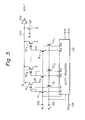
- Fig. 3 is a circuit diagram of a line image sensor constituting a first embodiment of the present invention.
- photosensor cells SCl - SCn of the structure shown in Fig. 1A have mutually connected collector electrodes 12.
- Capacitor electrodes 7 are connected, respectively through switching transistors Trl - Trn, to output terminals Srl - Srn for signal readout of a shift register 101, and further connected, respectively through switching transistors Tfl - Tfn, to output terminals Sfl - Sfn for refreshing of said shift register 101.
- the gates of the switching transistors Trl - Trn are commonly connected to a terminal 102, while those of the switching transistors Tfl - Tfn are commonly connected to a terminal 103.
- Said terminals 102 and 103 respectively receive two-phase clocks ⁇ 1 and ⁇ 2 to turn on and off said switching transistors in synchronization with said clock signals.
- the shift register 101 is connected with terminals 102, 103 and 104 to receive the above-mentioned clock signals ⁇ 1 and ⁇ 2 and to receive a start pulse PS from the terminal 104.
- the output terminals Srl - Srn of the shift register 101 in succession release signal reading pulses of a voltage Vr while the output terminals Sfl - Sfn release refreshing pulses of a voltage Vf as will be explained later.
- the emitter electrodes 8 of the photosensor cells SCl - SCn are commonly connected to a signal readout line 105, which is connected to an input terminal of an output amplifier 106 and is grounded through a switching transistor 107.
- Said switching transistor 107 is provided to dissipate the charge on the signal readout line, and receives, through the gate thereof, a clock signal ⁇ r determining the timing of charge dissipation.
- a start pulse PS is supplied to the shift register 101, and a clock signal ⁇ 1 is supplied to said shift register 101 and to the gate of the switching transistor Trl.
- the clock ⁇ 1 turns on the switching transistor Trl, and, in synchronization with said clock ⁇ 1 a signal readout pulse of a voltage Vr is released from the terminal Srl of the shift register 101.
- Said signal readout pulse is transmitted through the switching transistor Trl in the on-state and is supplied to the capacitor electrode 7 of the photosensor cell SCl.
- a signal readout operation as explained before whereby the emitter 8 of the photosensor cell SCl releases a signal representing optical information, which is supplied through the line 105 to the output terminal after amplification in the output amplifier 106.
- the switching transistor 107 Upon completion of signal readout from the photosensor cell SCl, the switching transistor 107 is turned on by the clock ⁇ r to ground the signal readout line 105, thus dissipating the charge accumulated in the wiring capacity. Simultaneously, in response to the clock ⁇ 2, the terminal Sfl of the shift register 101 releases a refreshing pulse of a voltage Vf, which is transmitted through the switching transistor Tfl turned on by said clock ⁇ 2 and supplied to the capacitor electrode 7. In this manner the charges accumulated in the photosensor cell SCl and in the signal readout line 105 are eliminated.
- the terminal Sr2 supplies a pulse of the voltage Vr to the capacitor electrode of the photosensor cell SC2, thus effecting the signal readout thereform.
- the photosensor cell SC2 is refreshed by a clock ⁇ 2, while the signal readout line 105 is refreshed by a clock ⁇ r.
- the optical information of all the photosensor cells SCl - SCn can be serially read by effecting the signal readout and refreshing for each photosensor cell in synchronization with the clocks ⁇ 1 and ⁇ 2. Since each photosensor cell is refreshed at the completion of the signal readout operation, the photosensor cells can collectively enter the accumulating operation when the signal readout and refreshing for the last cell SCn are completed. Thereafter the above-explained steps are repeated.
- Fig. 5A is a cross-sectional view of a photosensor cell constituting a second embodiment of the present invention
- Fig. 5B is an equivalent circuit diagram of said photosensor cell.
- the p-type area 4 is set at a determined potential by a MOS transistor to achieve complete refreshing.
- the refreshing MOS transistor is composed of main electrode areas consisting of a p-type area 4 and a p-type area 41 formed on an n ⁇ -type epitaxial layer 3, and the capacitor electrode 7 positioned across an oxide layer 6 serves as the gate.
- the MOS transistor is turned off when a positive voltage is supplied to the capacitor electrode 7 but is turned on to connect the electrode 42 with the p-type area 4 when a negative voltage exceeding a determined threshold value is supplied.
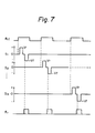
- Fig. 6 is a circuit diagram of an image sensor device constituting the second embodiment of the present invention.
- photosensor cells SCl - SCn are respectively provided with refreshing MOS transistors Tl - Tn.
- the capacitor electrodes 7 of the photosensor cells are connected, respectively through switching transistors Trfl - Trfn, to output terminals Sl - Sn of a shift register 201, and the gates of said transistors Trfl - Trfn are commonly connected to a terminal 202 for effecting on-off operations by clocks ⁇ rf .
- the shift register 201 releases a signal readout pulse of a positive voltage Vr and a succeeding refreshing pulse of a negative voltage -Vf, in succession, from the terminals Sl - Sn.
- Electrodes 42 of the photosensor cells SCl - SCn are commonly connected to a terminal 203, receiving a determined refreshing voltage Vrf.
- Other components same as those in the first embodiments are represented by same numbers and will not be explained further.
- the terminal Sl of the shift register 201 releases a signal readout pulse of a positive voltage Vr, which is supplied, through said switching transistor Trfl, to the capacitor electrode 7 of the photosensor cell SCl. Because of said positive voltage Vr the MOS transistor Tl remains turned off, and the photosensor cell SCl effects a signal readout operation explained above.
- the terminal Sl supplies a refreshing pulse of a negative voltage -Vf to the capacitor electrode 7 of said photosensor cell SCl to turn on the MOS transistor Tl, whereby the base area 4 releases the charge accumulated therein through the electrode 42 and is set at a determined potential Vrf.
- the switching transistor 107 is turned on to refresh the signal readout line 105.
- the present embodiment allows to arbitrarily select the potential of the base area 4 and to achieve complete refreshing by suitably selecting the refreshing voltage Vrf.
- MOS transistors Tl - Tn are formed in the photosensor cells, they may also be formed on the separating areas 2. It is also possible to form said separating area 2 with a semiconductor of the same conductive type as the base area 4 to achieve insulation by a p-n junction and to form a refreshing MOS transistor by maintaining said separating area at a potential Vrf.
- FIG. 8 there are shown phototransistors 801 l - 801 n ; capacitors 802 l - 802 n for respectively transmitting control signals to said phototransistors; sample-hold circuits 806 l - 806 n composed of MOS transistors 803 l - 803 n for on-off controlling the output signals from the emitters of the phototransistors 801 l - 801 n , capacitors 804 l - 804 n for accumulating said output signals, and MOS transistors 805 l - 805 n for controlling the readout of the output signals from said capacitors; a logic circuit 819 for controlling the on/off state of the MOS transistors 805 l - 805 n ; an amplifier 821 for output signal reading; a common output line; a MOS transistor 824 for dissipating the charge accumulated in the common output line 820; a positive voltage input terminal 818; a power supply input terminal 815; an output terminal 822;
- MOS transistors 803 l - 803 n , 805 l - 805 n and 824 are of n-channel type.
- the MOS transistors 803 l - 803 n are turned on by an H-level signal supplied to the control signal input terminal 816, while the MOS transistors 805 l - 805 n are turned on by H-level signals released from all the output terminals 807 l - 807 n of the logic circuit 819, and the MOS transistor 824 is turned on by an H-level signal entered from the input terminal 823, whereby all the emitters of the phototransistors 801 l - 801 n are grounded. Also a positive bias voltage is entered from the positive voltage input terminal 818 to positively bias all the collectors of the phototransistors 801 l - 801 n .
- the MOS transistors 803 l - 803 n are turned on by an H-level signal supplied to the control signal input terminal 816 while the MOS transistors 805 l - 805 n are turned off by L-level signals released from all the output terminals 807 l - 807 n of the logic circuit 819, whereby the emitters of the phototransistors 801 l -801 n are connected with the capacitors 804 l - 804 n . Also all the collectors of the phototransistors 801 l - 801 n are positively biased by a positive bias voltage supplied to the input terminal 818.
- a pulse of a positive voltage V RE is entered through the input terminal 817, whereby, in a photosensor cell irradiated by light, the base potential of the phototransistor becomes equal to a(V RE - V RF ) + ⁇ V B to obtain a collector current determined by the base current.
- the output voltage of the phototransistor representing the optical information, is held in the connected capacitor 804.
- the MOS transistors 803 l - 803 n are turned off by entering an L-level signal from the input terminal 816 and H-level signals are released in succession from the output terminals 807 l - 807 n of the logic circuit thereby turning on the MOS transistors 805 l - 805 n in succession.
- an H-level signal is entered through the input terminal 823 to turn on the MOS transistor 824, thereby discharging the capacitor after signal readout, and then the input terminal 823 is shifted again to the L-level to turn off the MOS transistor 824. In this manner the signal readout of a line can be achieved by effecting the signal readout operation from the sample hold circuits 806 l - 806 n to the output terminal 822 in succession.
- the time required for signal readout of a line is represented by t RE1 + n(t RE2 + t RE3 ) , wherein t RE1 represents a time required for signal readout from a phototransistor 801 i to the sample hold circuit 806 i , t RE2 is a time required for reading the voltage accumulated in the sample hold circuit 806 i through the output terminal 822, and t RE3 is a time required for discharging the capacitor 804 i of the sample hold circuit 806 i .
- Said readout time t RE2 from the capacitor 804 i to the output terminal 822 and said discharge time t RE3 are small because the MOS transistors 805 l - 805 n constituting the sample hold circuit 806 l - 806 n can be composed of high-speed switching MOS transistors.
- the phototransistors 801 l - 801 n have a certain amplifying function, but the emitter current is limited, if the photosensor cells are arranged at a high density, since the amount of carriers generated in the base area decreases due to a smaller size of the cell. Consequently the signal readout time t RE1 from the phototransistors is relatively large, compared to t RE2 and t RE3 .
- the readout time t RE1 from the phototransistors depends on the capacities of the capacitors 804 l -804 n , which in turn are determined by the floating capacity of the common output line 820.
- the signal readout time for a line is represented by n(t RE1 + t RE3 ) since the signal readout time from a photosensor cell 101 to the output terminal 22 is equal to the aforementioned time t RE1 for signal accumulating time in the capacitor 804 i , and the discharge time from the common output line 20 is likewise equal to t RE3 .
- t RE1 >> t RE3 .
- the MOS transistors 803 l - 803 n are turned by an H-level signal supplied to the input terminal 816, while the MOS transistors 805 l - 805 n are also turned by H-level signals released from all the output terminals 807 l -807 n of the logic circuit 819, and the MOS transistor 824 is also turned on by an H-level signal entered from the input terminal 823, whereby all the emitters of the phototransistors 801 l - 801 n are grounded.
- a positive bias voltage is entered from the positive voltage input terminal 818 to positively bias all the collectors of the phototransistors 801 l - 801 n .
- the refreshing operation is conducted by entering, in this state, a pulse of a positive voltage V RF through the control signal input terminal 817, whereby the base potential returns to the initial negative potential -aV RF .
- the function of the image line sensor is effected by repeating the above-explained steps of accumulation, readout and refreshing.
- the MOS transistors 803 l - 803 n , 805 l - 805 n and 824 are assumed to be of n-channel type, it is also possible to employ p-channel transistors or complementary transistors in which p-channel and n-channel transistors are combined.
- Fig. 9 is a circuit diagram of the fourth embodiment of the present invention, in which shown are phototransistors 901 ll - 901 mn and capacitors 902 ll - 902 mn for transmitting control signals to said phototransistors, both two-dimensionally arranged in n columns and m rows; and sample hold circuits 906 l -906 n composed of MOS transistors 903 l - 903 n for controlling the output signals from the emitters of the phototransistors 901 ll - 901 mn , capacitors 904 l -904 n connecting main electrodes of said MOS transistors 903 l - 903 n with a power input terminal 915, MOS transistors 909 l - 909 n of which gates are connected to the main electrodes of said MOS transistors 903 l - 903 n , MOS transistors 905 l - 905 n of which main electrodes are respectively connected to the MOS transistors 909 l - 9
- control signal input terminal 917 for supplying control signals to the photosensor cells; a control signal input terminal 916 for supplying control signals to the MOS transistors 903 l - 903 n ; a positive voltage input terminal 918; an output terminal 922; a control input terminal 926 for supplying control signals to the MOS transistors 910 l - 910 n ; and a power input terminal 927.
- the phototransistors 901 ll - 901 mn of the present invention achieve photoelectric conversion by a basic function consisting of an accumulation step, a signal readout step and a refreshing step.
- Fig. 9 it is assumed that all the MOS transistors are of n-channel type, that the positive voltage input terminal 918 and the power input terminal 925 receive positive voltages, and that the input terminals 915 and 927 are grounded.
- an H-level signal is supplied to the control input terminal 926 to turn on the MOS transistors 910 l - 910 n , thereby grounding all the emitters of the phototransistors 901 ll - 901 mn .
- a positive voltage is supplied to the input terminal 918 to positively bias all the collectors of said phototransistors, and a pulse of a positive voltage V RF is supplied from arbitrary one of the control signal input terminals 917 l - 917 n to bias the bases of the phototransistors 901 ll - 901 mn at a determined negative potential.
- V RF positive voltage
- the pulse for negatively biasing the bases of the phototransistors 901 ll - 901 mn may be given to a row or plural rows at a time.
- an H-level signal is supplied to the control signal input terminal 916 to turn on the MOS transistors 903 l - 903 n and an L-level signal is supplied to the control signal input terminal 926 to turn off the MOS transistors 910 l -910 n , whereby all the emitters of the phototransistors 901 ll - 901 mn are left open, and a positive bias voltage is supplied through the positive voltage input terminal 918 to positively bias all the collectors of the phototransistors 901 ll - 901 mn .
- pulses of a positive voltage V RE are supplied in an arbitrary or sequential order to the control signal input terminals 917 l - 907 m .
- the signal readout from the sample hold circuits 906 l - 906 n to the output terminal 922 is effected by supplying an L-level signal through the control input terminal 916 to turn off the MOS transistors 903 l - 903 n and releasing H-level signals in succession from the output terminals 907 l - 907 n of the logic circuit 919, thereby turning on the MOS transistors 905 l - 905 n in succession.
- the MOS transistor 905 l is turned on to apply the positive voltage at the terminal 925 to the MOS transistor 909 l . Consequently a current corresponding to the voltage applied to the gate is generated between the main electrodes of the MOS transistor 909 l , thus generating a voltage, across the resistor 908 l , corresponding to the accumulated voltage in the capacitor 904 l , and said voltage is released from the output terminal 922 as an optical information signal. Thereafter the voltages accumulated in the capacitors 904 l - 904 n are released in succession through the output terminal 922.
- the phototransistors 901 il - 901 in and the capacitors 904 l - 904 n are refreshed by entering an H-level signal to the control input terminal 916 to turn on the MOS transistors 903 l - 903 n and entering an H-level signal through the control input terminal 926 to turn on the MOS transistors 910 l - 910 n , whereby the capacitors 904 l - 904 n are discharged through the MOS transistors 903 l - 903 n and 910 l - 910 n .
- the phototransistors 901 il - 901 in are refreshed by applying a positive voltage to the input terminal 917 i .
- the phototransistors 901 il - 901 Upon completion of the refreshing operation explained above, the phototransistors 901 il - 901 in initiate the accumulating operation. Simultaneously the signal readout and refreshing are effected in the above-explained manner for the phototransistors 901 jl - 901 jn of a j-th row.
- optical information signals of each row are collectively held in the capacitors 904 l -904 n and then are serially released, it is possible to simultaneously effect the signal readout and refreshing of a row and the accumulation for other plural rows.
- the signal readout and refreshing need not necessarily be effected for each row but may be effected for plural rows at a time.
- the above-explained circuit of Fig. 9, constituting the fourth embodiment of the present invention is characterized by a fact that the refreshing and accumulation for different rows and the signal readout from the sample hold circuits can be simultaneously conducted. Consequently the photoelectric conversion can be achieved in a sequence in which the time from the refreshing to the signal readout is maintained constant in any row.
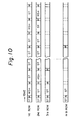
- Fig. 10 is a chart showing the operating sequence, for further clarifying the function of said fourth embodiment.
- R indicates the signal readout operation from the phototransistors to the sample hold circuits 906 l - 906 n ;
- RSH indicates a period of signal readout from the sample hold circuits 906 l - 906 n to the output terminal 922 and refreshing of the phototransistors;
- ST indicates the accumulating period;
- W indicates that the signal readout is conducted on certain phototransistors outside the row of said symbol W. More specifically, in the period W, the base of the phototransistor is maintained negative to effect the accumulating operation, but the emitter is shifted to a positive potential because the signal readout is conducted from the emitter of phototransistors of another row to the sample hold circuits.
- MOS transistors in the fourth embodiment shown in Fig. 9 are composed of N-channel MOS transistors, it is also possible to employ P-channel MOS transistors or complementary circuits in which N- and P-channel MOS transistors are combined. Also the cathode-follower amplifiers employed in the sample-hold circuits may be replaced by other amplifiers such as differential amplifiers.
- Figs. 11 and 12 illustrate the basic structure and function of a photosensor cell to be employed in the ensuing embodiments.
- Fig. 11A is a plan view of said photosensor cell
- Fig. 11B is a cross-sectional view thereof along a line A-A'
- Fig. 12 is an equivalent circuit thereof, wherein same components are always represented by same numbers.
- Fig. 11 there is shown an arrangement in rows and columns, but there may naturally be employed a staggered arrangement of pixels in order to improve the resolving power in the horizontal direction.
- Said photosensor cell is provided with a structure as explained in the following.
- a passivation layer 1102 there are provided, on an n-type silicon substrate 1102; a passivation layer 1102; an insulating oxide layer 1103 composed of silicon oxide; a separating area 1104 composed of an insulating layer or a polysilicon layer for electrically separating the neighboring photosensor cells; an n ⁇ -type area 1105 of a low impurity concentration formed for example by epitaxy; a p-type area 1106 formed thereon to constitute a base of a bipolar transistor; an n+-type area 1107 constituting an emitter of said bipolar transistor; a wiring 1108 composed of a conductive material such as aluminum for signal readout to the exterior; a capacitor electrode 1109 opposed to the p-type area 1106 across the insulator 1103 for applying pulses to said p-type area 1106 in the floating state; a wiring 1110 connected to said capacitor electrode 1109; an n+-type area 1111
- a capacitor C ox 1113 is composed, in a MOS structure, of the electrode 1109, insulating layer 1103 and p-type area 1106, while a bipolar transistor 1114 is composed of the n+-type area 1107 functioning as the emitter, p-type area 1106 functioning as the base and n ⁇ -type area 1105 and area 1101 functioning as the collector. Also as will be understood from these drawings, the p-type area 1106 is maintained in the float-state.
- the bipolar transistor 1114 is represented by a junction capacity Cbe 1115 of the base and emitter; a p-n junction diode Dbe 1116 between the base and emitter; a junction capacity Cbc 1117 between the base and collector; and a p-n junction diode Dbc 1118 between the base and collector.
- the basic function of said photosensor cell is composed, as already explained before, of a charge accumulation step in response to the incident light, a signal readout step and a refreshing step.
- the emitter is grounded through the wiring 1108, while the collector is positively biased through the wiring 1112.
- the base is in advance biased inversely to the emitter 1107.
- the potential Vp generated by the incident light remains almost constant even when the photosensor cell size is reduced to achieve a higher resolving power, since the amount of accumulated charge Q decreases with the decrease in the amount of light per cell while the junction capacity decreases proportional to the cell size.
- the photosensor cell of the present invention can have a very large effective light-receiving area, because of the very simple structure as shown in Fig. 11.
- the emitter and the wiring 1108 are maintained in the floating state, while the collector is maintained at a positive potential Vcc.
- the base potential is equal to -Vb + Vp, wherein -Vb is a negative bias potential of the base 1106 prior to light irradiation, and Vp is the accumulated voltage generated by said irradiation.
- a positive voltage Vr for signal reading is applied to the electrode 1109 through the wiring 1110.
- Said voltage is divided by the oxide layer capacity Cox 1113, base-emitter junction capacity Cbe 1115 and base-collector junction capacity Cbc 1117, so that the base potential is shifted to:
- the base potential is further biased in the forward direction, in comparison with the voltage Vp accumulated by the light irradiation. Consequently the electrons are injected from the emitter to the base, and reach the collector through acceleration by the drift electric field, because of the positive collector potential.
- the accumulated voltage Vp and the signal readout voltage are linearly proportional over a range in excess of 10,000 times, so that a high-speed signal readout is ensured if the readout time, in which the readout voltage Vr is applied to the capacitor electrode 1109, is selected longer than ca. 100 nsec.
- the wiring 1108 has a capacity of 4 pF while the junction capacity Cbe + Cbc is equal to 0.01 pF, with a ratio of ca. 300 times.
- the accumulated voltage Vp generated in the p-type area 1106 is not influenced, and an extremely speedy signal readout is rendered possible by the effect of the bias voltage Vbs. This is due to an effective contribution of the amplifying function of the photosensor cells. In comparison with such high output voltage, the fixed pattern noises and random noises resulting from the output capacity are relatively small, so that an extremely high S/N ratio can be obtained.
- Fig. 13B allows to know the signal readout time required by the readout voltage to reach a desired percentage of the accumulated voltage, at a given bias voltage Bvs. Consequently the chart shown in Fig. 13B allows to determine the required bias voltage Vbs, once the signal readout time and the linearity required for the overall design of the image sensor device are determined.
- Another advantage of the photosensor cell of the present invention is the possibility of non-destructive readout because the probability of recombination of electron and hole in the p-type area 1106 is quite low. This fact indicates the possibility of a new function in case said photosensor cells are constructed as an image sensor device.
- the p-type area 1106 can maintain the voltage Vp for an extremely long time, and the maximum holding time is rather limited by a dark current thermally generated in the depletion layer of the junction.
- the depletion layer is present in the n ⁇ -type area 1105 with a very low impurity concentration with a high crystallinity, so that few pairs of electrons and holes are thermally generated.
- the charge accumulated in the p-type area 1106 is not dissipated in the signal readout operation as already explained before. For this reason, in order to enter new optical information, the previously accumulated charge has to be dissipated in a refreshing operation. It is at the same time necessary to maintain the p-type area 1106 in the floating state at a determined negative potential.
- the refreshing operation is effected, just like the signal readout, by applying a positive voltage to the electrode 1109 through the wiring 1110. At the same time the emitter is grounded through the wiring 1108. The collector is grounded or maintained at a positive potential through the electrode 1112.
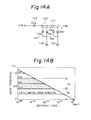
- Fig. 14A shows an equivalent circuit for refreshing operation, wherein the collector is grounded.
- a positive voltage Vrh is applied to the electrode 1109 in this state, a voltage: obtained by capacitative division through the oxide layer capacity Cox 1113, base-emitter junction capacity Cbe 1115 and base-collector junction capacity Cbc 1117, is instantaneously applied to the base 1122 as in the signal readout step. Said voltage forms a forward bias in the base-emitter junction diode Dbe 1116 and the base-collector junction diode Dbc 1118, thus generating currents therein, whereby the base potential is gradually lowered.
- Fig. 14B shows the result of calculation of change in the potential of floating base, as an example of time dependence of the base potential, wherein the abscissa indicates the refreshing time or the time after the application of the refreshing voltage Vrh to the electrode 1109, while the ordinate indicates the base potential, indicating various initial base potentials.
- the initial base potential is the potential of the floating base when the refreshing voltage Vrh is applied, and is determined by Vrh, Cox, Cbe, Cbe and the charge accumulated in the base.
- Fig. 14B indicates that the base potential is not determined by the initial potential but shows a linear change in logarithmic scale after the lapse of a determined time.
- the p-type area 1106 can be biased to a negative potential in two ways, by applying a positive voltage through the MOS capacitor Cox for a determined period and then removing said voltage. In one method, a negative charge is accumulated by the flow of positively charged holes from the p-type area 1106 to the n-type area 1101 in grounded state.
- the solid-state solid image sensor device employing the above-explained photosensor cells has a complete refreshing mode, in which the base potential of all the photosensor cells is brought to zero (requiring 10 seconds in the example shown in Fig. 14B), and a transient refreshing mode, in which a variable component resulting from the accumulated voltage Vp is dissipated though a certain base potential remains (requiring 10 ⁇ sec to 10 sec in the example shown in Fig. 14B.
- the complete refreshing mode or the transient refreshing mode is selected according to the purpose of use of the image sensor device.
- the photosensor cell explained above disclosed in the aforementioned European Patent Application Laid-open No. 0130276, is much simpler in structure than conventional photosensors thus providing an ample possibility for a higher resolving power in the future, and retains the advantages of a low noise level, a high output level, a wide dynamic range and a non-destructive signal readout resulting from the amplifying function.
- Fig. 15 is a circuit diagram of an embodiment of a solid-state image sensor device, composed of a one-dimensional array of the above-explained photosensor cells.
- Fig. 15 there are provided three photosensor cells 1530 of which collectors 1512 are commonly connected.
- Capacitor electrodes 1510 of said photosensor cells 1530 are connected to a horizontal line 1531 for supplying readout pulses and refreshing pulses.
- Said horizontal line 1531 is connected, through a buffer MOS transistor 1532, to a terminal 1533 for supplying refreshing pulses, and the gate of said buffer MOS transistor 1532 is connected to a terminal 1534.
- the horizontal line 1531 is connected, through a buffer MOS transistor 1535, to a terminal 1536 for supplying readout pulses, and the gate of said transistor is connected to a terminal 1537.
- Emitters 1508 of the photosensor cells 1530 are respectively connected to vertical lines 1538, 1538', 1538'' for signal readout for each column, and said vertical lines are connected, respectively through gate MOS transistors 1539, 1539', 1539'', to the input terminal of a P-type CCD register 1540.
- the gates of said gate MOS transistors 1539, 1539', 1539'' are connected to a terminal 1541 for generating pulses for controlling the vertical lines.
- the output terminal of the CCD register 1540 is connected to an output signal line 1542, which is grounded through a refreshing transistor 1543, whose gate is connected to a terminal 1544.
- Said output signal line 1542 is further connected to the gate of a signal amplifying transistor 1545, of which drain is connected to a load resistor 1546 and an output terminal 1547 for releasing the amplified output signals.
- the vertical lines 1538, 1538', 1538'' are grounded through refreshing MOS transistors 1548, 1548', 1548'', of which gates are commonly connected to a terminal 1549.
- the terminal 1549 is maintained at an H-level to turn on the MOS transistors 1548, 1548', 1548'' whereby the photosensor cells are grounded through the vertical lines 1538, 1538', 1538''.
- An H-level signal is also supplied to the terminal 1534 to turn on the refreshing MOS transistor 1532.
- a refreshing pulse supplied to the terminal 1533 is transmitted through the horizontal line 1531 to provide the bases of the photosensor cells with a voltage Vrh, whereby the refreshing operation is initiated to dissipate the accumulated charges according to the complete refreshing mode or the transient refreshing mode.
- the bases of the transistors of the photosensor cells are inversely biased with respect to the emitters, thus initiating a succeeding accumulation.
- all other pulses are maintained at an L-level state as will be understood from the drawing.
- the electrons of the electron-hole pairs generated by light irradiation can be rapidly dissipated into the collector since the substrate, or the collector of transistor, is maintained at a positive potential.
- the terminal 1549 is maintained at an H-level state as in the refreshing step to maintain the MOS transistors 1548, 1548', 1548'' in the conductive state, whereby the emitters of the photosensor cells are grounded through the vertical lines 1538, 1538', 1538''. If the base is saturated with holes under a strong light irradiation, or, if the base becomes biased in forward direction with respect to the grounded emitter potential, the holes flow through the vertical lines 1538, 1538', 1538'', so that the base potential no longer moves and is clipped in this state. Consequently the blooming phenomenon can be avoided by the grounding of the vertical lines, even though the emitters of vertically neighboring photosensor cells are commonly connected to the vertical lines 1538, 1538', 1538''.
- the signal readout period starts from a time t3, when the terminal 1549 is shifted to an L-level state, and terminal 1537 is shifted to an H-level state, thereby turning off the MOS transistors 1548, 1548', 1548'' and turning on the MOS transistor 1535.
- a readout pulse of a voltage Vr is supplied to the terminal 1536, whereby the signal readout from three photosensor cells connected to the horizontal line 1531 is effected through the MOS transistor 1535.
- an H-level signal is supplied to the terminal 1541 to turn on the MOS transistors 1539, 1539', 1539'', whereby the output signals of the photosensor cells are simultaneously supplied to the CCD registor 1540.
- Said output signals stored in the CCD register 1540 are transferred in succession, after the completion of the signal readout period, to the output signal line 1542, then amplified by the transistor 1545 and released through the output terminal 1547.
- a charge remains in the output signal lines 1542, due to a wiring capacity.
- an H-level signal is supplied to the terminal 1544 in synchronization with the transfer timing of the CCD register 1540, so that the output signals are transferred, in separated state, to the transistor 1545.
- the final amplifier can be made simpler in comparison with the MOS image sensor device since a high output voltage can be obtained by the amplifying function of each photosensor cell.
- the MOS transistor employed as the signal amplifier 1545 in the present embodiment can be naturally replaced by other amplifying means such as a bipolar transistor.
- an n-type CCD register may also be employed if the output charge from each photosensor cell is subtracted from a charge accumulated in advance in the register.
- the image sensor device of the present invention provides a higher output voltage, a higher sensitivity and a lower noise level, thus enabling to achieve a higher resolving power, in comparison with conventional MOS or CCD image sensor devices.
- the image sensor device of the present invention is capable of a high-speed signal readout operation even for an increased number of photosensor cells, thus providing a high-speed operation combined with a high resolving power, since the signals from plural photosensor cells are temporarily retained in holding means and then released sequentially.
- the photosensor cells can have a uniform accumulation time, thus ensuring a stable photoelectric converting characteristic, because each photosensor cell can be refreshed immediately after the signal readout operation. Also a high-speed operation is rendered possible because of the absence of idle time after the completion of signal readout as in the conventional structure.
- the image sensor device of the present invention can achieve a higher packing density because a pixel is composed of a single transistor, and still shows significantly reduced blooming and smear phenomena. It also provides a higher sensitivity and a wider dynamic range.
- the amplifying function of the photosensor cells themselves allows to obtain a high signal voltage without relying on the wiring capacity, to achieve a low noise level and facilitates the designing of peripheral circuits.
- the transfer of the output signals from the photosensor cells with a CCD register allows to achieve a higher packing density in comparison with the conventional structure involving complex shift registers, and easily achieves a transfer frequency in excess of 100 MHz required in high-speed signal processing.
Description
- The present invention relates to an image sensor device in which arranged one- or two-dimensionally are photoelectric converting elements (hereinafter called photosensor cells) each having a capacitor on the control electrode area of a semiconductor transistor.
- Recent developments on image sensor device have been principally conducted on CCD type and MOS type.
- The CCD image sensor device is based on a principle that potential wells are formed under MOS capacitor electrodes for accumulating electric charges generated by the entering light, and, in signal reading, said potential wells are moved in succession by pulses supplied to the electrodes thereby transferring the accumulated charges to an output amplifier. On the other hand, the MOS image sensor device is based on a principle that electric charges generated by the entering light are accumulated in photodiodes constituting a light-receiving area and each comprising a p-n junction, and, in signal reading, MOS switching transistors respectively connected to said photodiodes are turned on in succession to transfer the accumulated charges to an output amplifier.
- However such conventional image sensor devices have been associated with following drawbacks which will be a major obstacle in achieving a higher sensitivity and a higher resolving power in the future.
- More specifically, the CCD image sensor devices have drawbacks that (1) the MOS output amplifier formed on a same chip tends to generate, from the interface between silicon and a silicon oxide layer, l/f noises which are easily noticeable on the image. (2) the maximum charge that can be accumulated in a potential well is reduced and the dynamic range becomes smaller if the number of cells are increased with a higher density in order to achieve a higher resolving power, and (3) the sequential charge transfer is interrupted if only one cell is defective.
- On the other hand, the MOS image sensor devices have drawbacks that (1) a large drop in the signal voltage occurs at the signal reading since a wiring capacitance is connected to each photodiode, (2) a large wiring capacitance tends to generate random noises, and (3) noises of a fixed pattern are present because of fluctuation in the parasite capacitances of the MOS switching transistors. Thus, for example in a two-dimensional solid-state image sensor device, image taking under a low illumination becomes difficult, and a size reduction of the cells for achieving a higher density deteriorates the S/N ratio since the wiring capacitance is not significantly reduced while the accumulated charge becomes smaller.
- In this manner the CCD and MOS image sensor devices are associated with fundamental problems in achieving a higher resolving power. On the other hand, there has been proposed a new semiconductor image sensor device (European Patent Application published as EP-A-0132076 published after the present priority date) in which electric charges generated by the entering light are accumulated in control electrodes, for example bases of bipolar transistors or gates of static induction transistors (SIT) or MOS transistors, and the accumulated charges are amplified at signal reading by the amplifying function of the cells. This structure can provide a high output, a wide dynamic range, a low noise level and a non-destructive signal reading, thus leading to a possibility for a higher resolving power.
- However there is a certain limit in the resolving power since this structure, if employed in a two-dimensional image sensor device, is fundamentally based on x-y addressing, and each cell is basically composed of a conventional MOS cell combined with an amplifying element such as a bipolar transistor or a SIT transistor. Also in case a large number of cells are arranged for achieving a high resolving power, a high-speed function is difficult to achieve because shift registers for reading the output signals become complicated. Besides, the S/N ratio becomes lower though the output impedance becomes higher.
- Also a one-dimensional image sensor device is associated with certain drawbacks which will be explained in the following in relation to the accompanying drawings.
- Fig. 1 is a circuit diagram of a conventional one-dimentional image sensor device containing an array of plural photosensor cells, in which electric charges are accumulated in capacitors electrically connected to control electrode areas.
- Referring to Fig. 1, said
photosensor cells 101 are linearly arranged, and output terminals thereof are connected, through MOS transistors 5l - 5n, to acommon output line 20. Saidcommon output line 20 is connected to anoutput terminal 22 through anoutput amplifier 21, and is also grounded through a line-refreshingMOS transistor 24. The gates of the MOS transistors 5l - 5n are respectively connected to terminals 7l - 7n of alogic circuit 19. - In such conventional image sensor device, the optical information signals of the
photosensor cells 101 are serially released through thecommon output line 20 and theoutput amplifier 21 by serial activation of the MOS transistors 5l - 5n. - The time required for signal reading from a
photosensor cell 101 is proportional to the floating capacity of thecommon output line 20. Consequently, the total time required for signal reading rapidly increases with an increase in the number n of thephotosensor cells 101. - In this manner, in the conventional structure, the high-speed signal reading operation becomes difficult to achieve, when the number n of the photosensor cells is increased in order to achieve a high resolving power.
- Furthermore, in the above-explained
photosensor cell 101 in which the electric charge generated by photoexcitation is accumulated in the control electrode, the accumulated charge has to be dissipated for refreshing, after the signal reading is completed. Since such refreshing operation has been conducted at a time for all thephotosensor cells 101, so that, particularly in a two-dimensional image sensor device, the time from said refreshing operation to the start of signal reading is different for allphotosensor cells 101, and for this reason it has been difficult to achieve a high-speed operation and a uniform photoelectric converting property. - EP-A-0111346 discloses a one-dimensional linear imaging array in which each pixel is provided by an SIT. The control gate region of the SIT is capacitively coupled to a control electrode, and accumulates holes in response to light. When a bias voltage is applied to the drain of the SIT and a read-out signal is applied to the control gate via the capacitively coupled control electrode, a drain current flows in accordance with the intensity of incident light. The drain current results in a signal at an output terminal. After all the pixels in the array have been read, the potential of a shielding gate of each pixel is reset to a predetermined level. The shielding gate is provided to isolate adjacent pixels by a depletion layer.
- Two refresh methods are disclosed in EP-A-0111346. In the first, read-out is destructive and the photocarriers from the control gate are discharged to the source electrode during read-out. In the second, read-out is non-destructive, and after all the pixels have been read in turn they are refreshed simultaneously by applying a negative bias to the shielding gate, so that photocarriers are discharged from the control gate to the shielding gate through the highly resistive main body of the SIT.
- The present invention provides an image sensor device and a control circuit as set out in the independent claims attached hereto, optionally with the features set out in the dependent claims.
- An embodiment of the present invention seeks to provide an image sensor device which can easily provide a high output level, a high sensitivity, a low noise level and a high resolving power.
- An embodiment of the present invention seeks to provide an image sensor device capable of high-speed signal reading even when the number of the photosensor cells is increased.
- An embodiment of the present invention seeks to provide an image sensor device which is provided with a stable photoelectric converting property and provides a high output level, a resolving power and a high-speed signal reading operation.
- An embodiment of the present invention seeks to provide a solid-state image sensor device which allows to easily attain a high cell density and to obtain a wide dynamic range combined with significantly reduced blooming and smear.
-
- Fig. 1 is a circuit diagram of a conventional image sensor device;
- Fig. 2A is a cross-sectional view of a photosensor cell of a line sensor constituting an embodiment of the present invention, while Fig. 2B is an equivalent circuit diagram of said photosensor cell;
- Fig. 3 is a circuit diagram of a first embodiment of a line sensor of the present invention;
- Fig. 4 is a timing chart showing the function of said first embodiment;
- Fig. 5A is a cross-sectional view of a photosensor cell constituting a second embodiment of the present invention, while Fig. 5B is an equivalent circuit diagram of said photosensor cell;
- Fig. 6 is a circuit diagram of the second embodiment of the present invention;
- Fig. 7 is a timing chart showing the function of said second embodiment;
- Fig. 8 is a circuit diagram of a third embodiment of the image sensor device of the present invention;
- Fig. 9 is a circuit diagram of a fourth embodiment of the image sensor device of the present invention;
- Fig. 10 is a chart showing the function sequence of said fourth embodiment;
- Fig. 11A is a plan view of a photosensor cell of the present invention, while Fig. 11B is a cross-sectional view thereof along a line A-A';
- Fig. 12 is an equivalent circuit diagram of said photosensor cell;
- Fig. 13A is a chart showing the relation of the signal readout voltage to the accumulated voltage Vp for a bias voltage Vbs = 0.6 V; while Fig. 13B is a chart showing the relation of the signal reading time to said bias voltage Vbs;
- Fig. 14A is an equivalent circuit diagram of a photosensor cell at the refreshing operation, while Fig. 14B is a chart showing the change of base potential in relation to the refreshing time;
- Fig. 15 is a circuit diagram of a solid-state image sensor device composed of a linear array of the above-mentioned photosensor cells and constituting a fifth embodiment of the present invention; and
- Fig. 16 is a timing chart showing the function of said embodiment.
- Now the present invention will be clarified in detail by embodiments thereof shown in the accompanying drawings.
- Fig. 2A is a cross-sectional view of a photosensor cell in a first embodiment of a line image sensor device of the present invention, and Fig. 2B is an equivalent circuit diagram of said photosensor cell.
- Referring to Fig. 2A, on a
silicon substrate 1 which is rendered n or n+ type by doping with an impurity such as phosphor (P), antimony (Sb) or arsenic (As), there are formed an array of photosensor cells each of which is electrically insulated from the neighboring ones by means of separatingareas 2 composed of SiO₂, Si₃N₄ or polysilicon. On the photosensor cells there is formed apassivation layer 13 composed for example of a PSG layer. - The structure of each photosensor cell is as follows. On an n⁻-
type area 3 of a low impurity concentration formed for example by epitaxy, a p-type area 4 is formed by doping with a p-type impurity, and, in a part of said p-type area 4 there is formed an n⁺-type area 5 by impurity diffusion or by ion implantation. Said p-type area 4 and n⁺-type area 5 respectively constitute the base and emitter of a bipolar transistor. - Above said n⁻-
type area 3 there is formed anoxide layer 6, on which formed is acapacitor electrode 7 of a determined area. Saidcapacitor electrode 7 faces said p-type area 4 across anoxide layer 8, whereby the potential of the floating p-type area 4 can be controlled by pulse voltages applied to thecapacitor electrode 7. There are further provided anemitter electrode 8 connected to the n⁺-type area 5; an unrepresented wiring for releasing the signals to the exterior from saidemitter electrode 8; an unrepresented wiring connected to thecapacitor electrode 7; an n⁺-type area 11 of a high impurity concentration formed on the rear face of thesubstrate 1; and anelectrode 12 for supplying a potential to the collector of the bipolar transistor. - In the following there will be explained the basic function.
Light 13 irradiates the p-type area 4 constituting the base of the bipolar transistor, whereby a charge, composed of holes in this case, corresponding to the quantity of incident light, is accumulated in the p-type area 4 (accumulating operation). - The accumulated holes shift the base potential to positive. Then a positive signal reading voltage Vr is applied to the
capacitor electrode 7 to bias the p-type area 4 positively, whereby the p-type area 4 in which the holes are accumulated is biased in forward direction with respect to the n⁺-type area 5. Thus a current by electrons flows from the n⁺-type area 5 to the n⁻-type area 3, so that the n⁺-type area 5 and theemitter electrode 8 in the floating state shows an increase in the potential. Thus an electric signal corresponding to the amount of incident light can be obtained by reading said change in the potential of the emitter electrode 8 (signal reading operation). - The charge accumulated in the p-
type area 4 can be eliminated by grounding theemitter electrode 8 and applying a positive pulse of a positive voltage Vf to thecapacitor electrode 7, whereby the p-type area 4 is biased in the forward direction with respect to the n⁺-type area 5 and the accumulated charge is dissipated (refreshing operation). Thereafter the above-mentioned steps of accumulation, readout and refreshing are repeated. - In short, the above-explained photosensor cell is based on a principle that the electric charge generated by the incident light is accumulated in the p-
type area 4 constituting the base, and the current from theemitter 8 to thecollector 12 is controlled by thus accumulated charge. Consequently the charge is read after an amplification by the amplifying function of each cell. This process provides a high output level, a high sensitivity and a low noise level and is promising for a higher resolving power in the future. - Fig. 3 is a circuit diagram of a line image sensor constituting a first embodiment of the present invention. In Fig. 3, photosensor cells SCl - SCn of the structure shown in Fig. 1A have mutually connected
collector electrodes 12.Capacitor electrodes 7 are connected, respectively through switching transistors Trl - Trn, to output terminals Srl - Srn for signal readout of ashift register 101, and further connected, respectively through switching transistors Tfl - Tfn, to output terminals Sfl - Sfn for refreshing of saidshift register 101. - The gates of the switching transistors Trl - Trn are commonly connected to a terminal 102, while those of the switching transistors Tfl - Tfn are commonly connected to a terminal 103. Said
terminals - The
shift register 101 is connected withterminals shift register 101 in succession release signal reading pulses of a voltage Vr while the output terminals Sfl - Sfn release refreshing pulses of a voltage Vf as will be explained later. - The
emitter electrodes 8 of the photosensor cells SCl - SCn are commonly connected to asignal readout line 105, which is connected to an input terminal of anoutput amplifier 106 and is grounded through a switchingtransistor 107. Said switchingtransistor 107 is provided to dissipate the charge on the signal readout line, and receives, through the gate thereof, a clock signal ør determining the timing of charge dissipation. - In the following there will be given an explanation on the function of the above-explained embodiment, while making reference to a timing chart shown in Fig. 4.
- It is assumed that charges corresponding to the incident light are already stored in the
base areas 4 of the photosensor cells SCl - SCn through the accumulating step explained above. - At first a start pulse PS is supplied to the
shift register 101, and a clock signal ø1 is supplied to saidshift register 101 and to the gate of the switching transistor Trl. The clock ø1 turns on the switching transistor Trl, and, in synchronization with said clock ø1 a signal readout pulse of a voltage Vr is released from the terminal Srl of theshift register 101. Said signal readout pulse is transmitted through the switching transistor Trl in the on-state and is supplied to thecapacitor electrode 7 of the photosensor cell SCl. In response there is conducted a signal readout operation as explained before whereby theemitter 8 of the photosensor cell SCl releases a signal representing optical information, which is supplied through theline 105 to the output terminal after amplification in theoutput amplifier 106. - Upon completion of signal readout from the photosensor cell SCl, the switching
transistor 107 is turned on by the clock ør to ground thesignal readout line 105, thus dissipating the charge accumulated in the wiring capacity. Simultaneously, in response to the clock ø2, the terminal Sfl of theshift register 101 releases a refreshing pulse of a voltage Vf, which is transmitted through the switching transistor Tfl turned on by said clock ø2 and supplied to thecapacitor electrode 7. In this manner the charges accumulated in the photosensor cell SCl and in thesignal readout line 105 are eliminated. - Subsequently, in response to a clock ø1, the terminal Sr2 supplies a pulse of the voltage Vr to the capacitor electrode of the photosensor cell SC2, thus effecting the signal readout thereform. Upon completion of said signal readout, the photosensor cell SC2 is refreshed by a clock ø2, while the
signal readout line 105 is refreshed by a clock ør. - In this manner the optical information of all the photosensor cells SCl - SCn can be serially read by effecting the signal readout and refreshing for each photosensor cell in synchronization with the clocks ø1 and ø2. Since each photosensor cell is refreshed at the completion of the signal readout operation, the photosensor cells can collectively enter the accumulating operation when the signal readout and refreshing for the last cell SCn are completed. Thereafter the above-explained steps are repeated.
- Fig. 5A is a cross-sectional view of a photosensor cell constituting a second embodiment of the present invention, and Fig. 5B is an equivalent circuit diagram of said photosensor cell.
- In the present embodiment, at the elimination of the accumulated holes, the p-
type area 4 is set at a determined potential by a MOS transistor to achieve complete refreshing. As shown in Fig. 5A, the refreshing MOS transistor is composed of main electrode areas consisting of a p-type area 4 and a p-type area 41 formed on an n⁻-type epitaxial layer 3, and thecapacitor electrode 7 positioned across anoxide layer 6 serves as the gate. - Thus, in the present embodiment, the MOS transistor is turned off when a positive voltage is supplied to the
capacitor electrode 7 but is turned on to connect theelectrode 42 with the p-type area 4 when a negative voltage exceeding a determined threshold value is supplied. - Fig. 6 is a circuit diagram of an image sensor device constituting the second embodiment of the present invention. In Fig. 6, photosensor cells SCl - SCn are respectively provided with refreshing MOS transistors Tl - Tn. The
capacitor electrodes 7 of the photosensor cells are connected, respectively through switching transistors Trfl - Trfn, to output terminals Sl - Sn of ashift register 201, and the gates of said transistors Trfl - Trfn are commonly connected to a terminal 202 for effecting on-off operations by clocks ørf. - In synchronization with said clocks ørf, the
shift register 201 releases a signal readout pulse of a positive voltage Vr and a succeeding refreshing pulse of a negative voltage -Vf, in succession, from the terminals Sl - Sn. -
Electrodes 42 of the photosensor cells SCl - SCn are commonly connected to a terminal 203, receiving a determined refreshing voltage Vrf. Other components same as those in the first embodiments are represented by same numbers and will not be explained further. - In the following there will be given an explanation on the function of the above-explained second embodiment, while making reference to a timing chart shown in Fig. 7.
- When the switching transistor Trfl is turned on by a clock ørf, the terminal Sl of the
shift register 201 releases a signal readout pulse of a positive voltage Vr, which is supplied, through said switching transistor Trfl, to thecapacitor electrode 7 of the photosensor cell SCl. Because of said positive voltage Vr the MOS transistor Tl remains turned off, and the photosensor cell SCl effects a signal readout operation explained above. - Subsequently the terminal Sl supplies a refreshing pulse of a negative voltage -Vf to the
capacitor electrode 7 of said photosensor cell SCl to turn on the MOS transistor Tl, whereby thebase area 4 releases the charge accumulated therein through theelectrode 42 and is set at a determined potential Vrf. Simultaneously with said refreshing operation, the switchingtransistor 107 is turned on to refresh thesignal readout line 105. - The above-explained operations are effected in succession in the photosensor cells SCl - SCn and the optical information is serially released from the output terminal.
- The present embodiment allows to arbitrarily select the potential of the
base area 4 and to achieve complete refreshing by suitably selecting the refreshing voltage Vrf. - Though the MOS transistors Tl - Tn are formed in the photosensor cells, they may also be formed on the
separating areas 2. It is also possible to form said separatingarea 2 with a semiconductor of the same conductive type as thebase area 4 to achieve insulation by a p-n junction and to form a refreshing MOS transistor by maintaining said separating area at a potential Vrf. - In the following there will be explained a third embodiment of the present invention, employing the photosensor cells of a structure shown in Fig. 1A.
- In Fig. 8, there are shown phototransistors 801l - 801n; capacitors 802l - 802n for respectively transmitting control signals to said phototransistors; sample-hold circuits 806l - 806n composed of MOS transistors 803l - 803n for on-off controlling the output signals from the emitters of the phototransistors 801l - 801n, capacitors 804l - 804n for accumulating said output signals, and MOS transistors 805l - 805n for controlling the readout of the output signals from said capacitors; a
logic circuit 819 for controlling the on/off state of the MOS transistors 805l - 805n; anamplifier 821 for output signal reading; a common output line; aMOS transistor 824 for dissipating the charge accumulated in thecommon output line 820; a positive voltage input terminal 818; a powersupply input terminal 815; anoutput terminal 822; acontrol input terminal 823 for supplying a control signal to theMOS transistor 824; a controlsignal input terminal 816 for supplying control signals to the MOS transistors 803l - 803n; a controlsignal input terminal 817 for supplying control signals to the capacitors 802l - 802n; and output terminals 807l - 807n of the logic circuit. - In the following explained is the function of the third embodiment of the present invention. It is assumed that the MOS transistors 803l - 803n , 805l - 805n and 824 are of n-channel type.
- In the accumulation step, the MOS transistors 803l - 803n are turned on by an H-level signal supplied to the control
signal input terminal 816, while the MOS transistors 805l - 805n are turned on by H-level signals released from all the output terminals 807l - 807n of thelogic circuit 819, and theMOS transistor 824 is turned on by an H-level signal entered from theinput terminal 823, whereby all the emitters of the phototransistors 801l - 801n are grounded. Also a positive bias voltage is entered from the positive voltage input terminal 818 to positively bias all the collectors of the phototransistors 801l - 801n. - On the other hand, all the bases of said phototransistors 801l - 801n are biased at a negative potential -aVRF by a refreshing operation to be explained later. In this state the photosensor cells are irradiated with light to accumulate holes in the bases thereof. The voltage accumulated in the base is represented as ΔVB.
- In the signal readout operation, the MOS transistors 803l - 803n are turned on by an H-level signal supplied to the control
signal input terminal 816 while the MOS transistors 805l - 805n are turned off by L-level signals released from all the output terminals 807l - 807n of thelogic circuit 819, whereby the emitters of the phototransistors 801l -801n are connected with the capacitors 804l - 804n. Also all the collectors of the phototransistors 801l - 801n are positively biased by a positive bias voltage supplied to the input terminal 818. In this state a pulse of a positive voltage VRE is entered through theinput terminal 817, whereby, in a photosensor cell irradiated by light, the base potential of the phototransistor becomes equal to to obtain a collector current determined by the base current. Thus the output voltage of the phototransistor, representing the optical information, is held in the connected capacitor 804. On the other hand, in the photosensor cell not irradiated with light, the base voltage of the phototransistor is equal to a(


- For reading the voltages held in the capacitors 804l - 804n through the output terminal 832, the MOS transistors 803l - 803n are turned off by entering an L-level signal from the
input terminal 816 and H-level signals are released in succession from the output terminals 807l - 807n of the logic circuit thereby turning on the MOS transistors 805l - 805n in succession. At each readout of the accumulated voltage from theoutput terminal 822 through theamplifier 821, an H-level signal is entered through theinput terminal 823 to turn on theMOS transistor 824, thereby discharging the capacitor after signal readout, and then theinput terminal 823 is shifted again to the L-level to turn off theMOS transistor 824. In this manner the signal readout of a line can be achieved by effecting the signal readout operation from the sample hold circuits 806l - 806n to theoutput terminal 822 in succession. - The time required for signal readout of a line is represented by

output terminal 822, and tRE3 is a time required for discharging the capacitor 804i of the sample hold circuit 806i. Said readout time tRE2 from the capacitor 804i to theoutput terminal 822 and said discharge time tRE3 are small because the MOS transistors 805l - 805n constituting the sample hold circuit 806l - 806n can be composed of high-speed switching MOS transistors. On the other hand, the phototransistors 801l - 801n have a certain amplifying function, but the emitter current is limited, if the photosensor cells are arranged at a high density, since the amount of carriers generated in the base area decreases due to a smaller size of the cell. Consequently the signal readout time tRE1 from the phototransistors is relatively large, compared to tRE2 and tRE3. - The readout time tRE1 from the phototransistors depends on the capacities of the capacitors 804l -804n, which in turn are determined by the floating capacity of the
common output line 820. - In the following the signal readout time of a line of the present embodiment, when the capacities of the capacitors 804l - 804n are selected equal to the floating capacity of the
common output line 820, is compared with the signal readout time of a line in the conventional structure shown in Fig. 1. - In the conventional structure shown in Fig. 1, the signal readout time for a line is represented by n(tRE1 + tRE3) since the signal readout time from a
photosensor cell 101 to theoutput terminal 22 is equal to the aforementioned time tRE1 for signal accumulating time in the capacitor 804i, and the discharge time from thecommon output line 20 is likewise equal to tRE3. Similar to the aforementioned third embodiment, tRE1 >> tRE3. For example, in a line sensor with a large value of n, the comparison of signal readout times leads to a conclusion

- Then, in the refreshing step, the MOS transistors 803l - 803n are turned by an H-level signal supplied to the
input terminal 816, while the MOS transistors 805l - 805n are also turned by H-level signals released from all the output terminals 807l -807n of thelogic circuit 819, and theMOS transistor 824 is also turned on by an H-level signal entered from theinput terminal 823, whereby all the emitters of the phototransistors 801l - 801n are grounded. In addition a positive bias voltage is entered from the positive voltage input terminal 818 to positively bias all the collectors of the phototransistors 801l - 801n. The refreshing operation is conducted by entering, in this state, a pulse of a positive voltage VRF through the controlsignal input terminal 817, whereby the base potential returns to the initial negative potential -aVRF. - The function of the image line sensor is effected by repeating the above-explained steps of accumulation, readout and refreshing.
- In the present third embodiment, the MOS transistors 803l - 803n, 805l - 805n and 824 are assumed to be of n-channel type, it is also possible to employ p-channel transistors or complementary transistors in which p-channel and n-channel transistors are combined.
- In the following there will be explained a fourth embodiment of the present invention.
- Fig. 9 is a circuit diagram of the fourth embodiment of the present invention, in which shown are phototransistors 901ll - 901mn and capacitors 902ll - 902mn for transmitting control signals to said phototransistors, both two-dimensionally arranged in n columns and m rows; and sample hold circuits 906l -906n composed of MOS transistors 903l - 903n for controlling the output signals from the emitters of the phototransistors 901ll - 901mn, capacitors 904l -904n connecting main electrodes of said MOS transistors 903l - 903n with a
power input terminal 915, MOS transistors 909l - 909n of which gates are connected to the main electrodes of said MOS transistors 903l - 903n, MOS transistors 905l - 905n of which main electrodes are respectively connected to the MOS transistors 909l - 909n and to thepower input terminal 925 and of which gates are respectively connected to the terminals 907l - 907n of alogic circuit 919, and resistors 908l - 908n connected at ends thereof to the other main electrodes of the MOS transistors 909l - 909n and to acommon output line 920 and connected at the other ends to thepower input terminal 915. There are further provided a control signal input terminal 917 for supplying control signals to the photosensor cells; a control signal input terminal 916 for supplying control signals to the MOS transistors 903l - 903n; a positivevoltage input terminal 918; anoutput terminal 922; a control input terminal 926 for supplying control signals to the MOS transistors 910l - 910n; and a power input terminal 927. - In the following there will be explained the function of the fourth embodiment shown in Fig. 9.
- As already explained before, the phototransistors 901ll - 901mn of the present invention achieve photoelectric conversion by a basic function consisting of an accumulation step, a signal readout step and a refreshing step. In Fig. 9 it is assumed that all the MOS transistors are of n-channel type, that the positive
voltage input terminal 918 and thepower input terminal 925 receive positive voltages, and that theinput terminals 915 and 927 are grounded. - In the accumulation step, an H-level signal is supplied to the control input terminal 926 to turn on the MOS transistors 910l - 910n, thereby grounding all the emitters of the phototransistors 901ll - 901mn. Also a positive voltage is supplied to the
input terminal 918 to positively bias all the collectors of said phototransistors, and a pulse of a positive voltage VRF is supplied from arbitrary one of the control signal input terminals 917l - 917n to bias the bases of the phototransistors 901ll - 901mn at a determined negative potential. In this state the photosensor cells are irradiated with light to accumulate holes in the base areas. - The pulse for negatively biasing the bases of the phototransistors 901ll - 901mn may be given to a row or plural rows at a time.
- In the signal readout, an H-level signal is supplied to the control signal input terminal 916 to turn on the MOS transistors 903l - 903n and an L-level signal is supplied to the control signal input terminal 926 to turn off the MOS transistors 910l -910n, whereby all the emitters of the phototransistors 901ll - 901mn are left open, and a positive bias voltage is supplied through the positive
voltage input terminal 918 to positively bias all the collectors of the phototransistors 901ll - 901mn. In this state pulses of a positive voltage VRE are supplied in an arbitrary or sequential order to the control signal input terminals 917l - 907m. - When the pulse of voltage VRE is supplied to an input terminal 917i, the outputs of the phototransistors 901il - 901in are held in the capacitors 904l - 904n of the sample hold circuits 906l - 906n and the accumulated voltages in said capacitors 904l - 904n are applied to the gates of the MOS transistors 909l - 909n.
- The signal readout from the sample hold circuits 906l - 906n to the
output terminal 922 is effected by supplying an L-level signal through the control input terminal 916 to turn off the MOS transistors 903l - 903n and releasing H-level signals in succession from the output terminals 907l - 907n of thelogic circuit 919, thereby turning on the MOS transistors 905l - 905n in succession. - Thus, in response to an H-level signal from the
output terminal 907l of thelogic circuit 919, the MOS transistor 905l is turned on to apply the positive voltage at the terminal 925 to the MOS transistor 909l. Consequently a current corresponding to the voltage applied to the gate is generated between the main electrodes of the MOS transistor 909l, thus generating a voltage, across theresistor 908l, corresponding to the accumulated voltage in thecapacitor 904l, and said voltage is released from theoutput terminal 922 as an optical information signal. Thereafter the voltages accumulated in the capacitors 904l - 904n are released in succession through theoutput terminal 922. - After the signal readout of an i-th row, the phototransistors 901il - 901in and the capacitors 904l - 904n are refreshed by entering an H-level signal to the control input terminal 916 to turn on the MOS transistors 903l - 903n and entering an H-level signal through the control input terminal 926 to turn on the MOS transistors 910l - 910n, whereby the capacitors 904l - 904n are discharged through the MOS transistors 903l - 903n and 910l - 910n. Similarly the phototransistors 901il - 901in are refreshed by applying a positive voltage to the input terminal 917i.
- Upon completion of the refreshing operation explained above, the phototransistors 901il - 901in initiate the accumulating operation. Simultaneously the signal readout and refreshing are effected in the above-explained manner for the phototransistors 901jl - 901jn of a j-th row.
- Since the optical information signals of each row are collectively held in the capacitors 904l -904n and then are serially released, it is possible to simultaneously effect the signal readout and refreshing of a row and the accumulation for other plural rows.
- The signal readout and refreshing need not necessarily be effected for each row but may be effected for plural rows at a time.
- The above-explained circuit of Fig. 9, constituting the fourth embodiment of the present invention, is characterized by a fact that the refreshing and accumulation for different rows and the signal readout from the sample hold circuits can be simultaneously conducted. Consequently the photoelectric conversion can be achieved in a sequence in which the time from the refreshing to the signal readout is maintained constant in any row.
- Fig. 10 is a chart showing the operating sequence, for further clarifying the function of said fourth embodiment.
- In Fig. 10, R indicates the signal readout operation from the phototransistors to the sample hold circuits 906l - 906n; RSH indicates a period of signal readout from the sample hold circuits 906l - 906n to the
output terminal 922 and refreshing of the phototransistors; ST indicates the accumulating period; and W indicates that the signal readout is conducted on certain phototransistors outside the row of said symbol W. More specifically, in the period W, the base of the phototransistor is maintained negative to effect the accumulating operation, but the emitter is shifted to a positive potential because the signal readout is conducted from the emitter of phototransistors of another row to the sample hold circuits. However the potentials of the emitter and base are still maintained in an inverse bias state, as in the accumulation. In Fig. 10 it is particularly noteworthy that the distance between two neighboring R's is constant in any row, and this fact is particularly meaningful when the number m of rows is increased, or when the number of photosensor cells is increased. There is required a long time for the signal readout from the 1st row to the last m-th row if the number M of row is large. Thus, if the accumulation and readout are effected after simultaneous refreshing for all rows, the last row will have a longer accumulation time and will therefore show a different photoelectric converting characteristic in comparison with the first row. Such drawback does not appear in the circuit of Fig. 9 and sequence of Fig. 10 as the period from refreshing to signal readout is constant in any row. Though the MOS transistors in the fourth embodiment shown in Fig. 9 are composed of N-channel MOS transistors, it is also possible to employ P-channel MOS transistors or complementary circuits in which N- and P-channel MOS transistors are combined. Also the cathode-follower amplifiers employed in the sample-hold circuits may be replaced by other amplifiers such as differential amplifiers. - In the following there will be explained still other embodiments of the present invention.
- Figs. 11 and 12 illustrate the basic structure and function of a photosensor cell to be employed in the ensuing embodiments.
- Fig. 11A is a plan view of said photosensor cell, Fig. 11B is a cross-sectional view thereof along a line A-A', and Fig. 12 is an equivalent circuit thereof, wherein same components are always represented by same numbers.
- In Fig. 11 there is shown an arrangement in rows and columns, but there may naturally be employed a staggered arrangement of pixels in order to improve the resolving power in the horizontal direction.
- Said photosensor cell is provided with a structure as explained in the following. As shown in Figs. 11A and 11B, there are provided, on an n-
type silicon substrate 1102;
apassivation layer 1102;
an insulatingoxide layer 1103 composed of silicon oxide;
aseparating area 1104 composed of an insulating layer or a polysilicon layer for electrically separating the neighboring photosensor cells;
an n⁻-type area 1105 of a low impurity concentration formed for example by epitaxy;
a p-type area 1106 formed thereon to constitute a base of a bipolar transistor;
an n⁺-type area 1107 constituting an emitter of said bipolar transistor;
awiring 1108 composed of a conductive material such as aluminum for signal readout to the exterior;
acapacitor electrode 1109 opposed to the p-type area 1106 across theinsulator 1103 for applying pulses to said p-type area 1106 in the floating state;
awiring 1110 connected to saidcapacitor electrode 1109;
an n⁺-type area 1111 formed on the bottom face of thesubstrate 1101 for making ohmic contact; and
anelectrode 1112 for supplying a collector potential to said bipolar transistor. - In the equivalent circuit shown in Fig. 12, a
capacitor C ox 1113 is composed, in a MOS structure, of theelectrode 1109, insulatinglayer 1103 and p-type area 1106, while abipolar transistor 1114 is composed of the n⁺-type area 1107 functioning as the emitter, p-type area 1106 functioning as the base and n⁻-type area 1105 andarea 1101 functioning as the collector. Also as will be understood from these drawings, the p-type area 1106 is maintained in the float-state. - In the equivalent circuit, the
bipolar transistor 1114 is represented by a junction capacity Cbe 1115 of the base and emitter; a p-njunction diode Dbe 1116 between the base and emitter; ajunction capacity Cbc 1117 between the base and collector; and a p-njunction diode Dbc 1118 between the base and collector. - In the following the above-explained photosensor cell will be clarified in further detail, in particular relation to other embodiments to be explained later.
- The basic function of said photosensor cell is composed, as already explained before, of a charge accumulation step in response to the incident light, a signal readout step and a refreshing step. In the charge accumulation, the emitter is grounded through the
wiring 1108, while the collector is positively biased through thewiring 1112. The base is in advance biased inversely to theemitter 1107. - In such state, as shown in Fig. 11, in response to the entry of light 1120 from the top face of the photosensor cell, a pair of electron and hole is generated in the semiconductor. The electrons flow toward the n-
type area 1101 because of the positive bias thereof, but the holes are accumulated in the p-type area 1106, whereby the potential thereof gradually changes toward positive side. The potential Vp caused by the accumulation of photo-generated holes in the base is given by
Cbe 1115 andCbc 1117. - It is to be noted that the potential Vp generated by the incident light remains almost constant even when the photosensor cell size is reduced to achieve a higher resolving power, since the amount of accumulated charge Q decreases with the decrease in the amount of light per cell while the junction capacity decreases proportional to the cell size. This is due to a fact that the photosensor cell of the present invention can have a very large effective light-receiving area, because of the very simple structure as shown in Fig. 11.
- In the following there will be explained an operation of reading a voltage generated by the charge accumulated in the p-
type area 1106. - In the signal readout step, the emitter and the
wiring 1108 are maintained in the floating state, while the collector is maintained at a positive potential Vcc. - In this state the base potential is equal to -Vb + Vp, wherein -Vb is a negative bias potential of the
base 1106 prior to light irradiation, and Vp is the accumulated voltage generated by said irradiation. Then a positive voltage Vr for signal reading is applied to theelectrode 1109 through thewiring 1110. Said voltage is divided by the oxidelayer capacity Cox 1113, base-emitter junction capacity Cbe 1115 and base-collectorjunction capacity Cbc 1117, so that the base potential is shifted to:
With a following additional forward bias Vbs:
the base potential is further biased in the forward direction, in comparison with the voltage Vp accumulated by the light irradiation. Consequently the electrons are injected from the emitter to the base, and reach the collector through acceleration by the drift electric field, because of the positive collector potential. - Fig. 13A is a chart showing the relation between the accumulated voltage Vp in case of Vbs = 0.6 V and the signal readout voltage.
- It will be understood, from said chart, that the accumulated voltage Vp and the signal readout voltage are linearly proportional over a range in excess of 10,000 times, so that a high-speed signal readout is ensured if the readout time, in which the readout voltage Vr is applied to the
capacitor electrode 1109, is selected longer than ca. 100 nsec. In the foregoing example, thewiring 1108 has a capacity of 4 pF while the junction capacity Cbe + Cbc is equal to 0.01 pF, with a ratio of ca. 300 times. However the accumulated voltage Vp generated in the p-type area 1106 is not influenced, and an extremely speedy signal readout is rendered possible by the effect of the bias voltage Vbs. This is due to an effective contribution of the amplifying function of the photosensor cells. In comparison with such high output voltage, the fixed pattern noises and random noises resulting from the output capacity are relatively small, so that an extremely high S/N ratio can be obtained. - It was already explained that a linearity over a range of ca. 10,000 times could be obtained with a high-speed signal readout time of ca. 100 nsec when the bias voltage Vbs is selected equal to 0.6 V. Fig. 13B shows this linearity and the relationship between the signal readout time and the bias voltage Vbs.
- Fig. 13B allows to know the signal readout time required by the readout voltage to reach a desired percentage of the accumulated voltage, at a given bias voltage Bvs. Consequently the chart shown in Fig. 13B allows to determine the required bias voltage Vbs, once the signal readout time and the linearity required for the overall design of the image sensor device are determined.
- Another advantage of the photosensor cell of the present invention is the possibility of non-destructive readout because the probability of recombination of electron and hole in the p-
type area 1106 is quite low. This fact indicates the possibility of a new function in case said photosensor cells are constructed as an image sensor device. - The p-
type area 1106 can maintain the voltage Vp for an extremely long time, and the maximum holding time is rather limited by a dark current thermally generated in the depletion layer of the junction. However, in said photosensor cell, the depletion layer is present in the n⁻-type area 1105 with a very low impurity concentration with a high crystallinity, so that few pairs of electrons and holes are thermally generated. - In the following there will be explained a process of dissipating the charge accumulated in the p-
type area 1106. - In the above-explained photosensor cell, the charge accumulated in the p-
type area 1106 is not dissipated in the signal readout operation as already explained before. For this reason, in order to enter new optical information, the previously accumulated charge has to be dissipated in a refreshing operation. It is at the same time necessary to maintain the p-type area 1106 in the floating state at a determined negative potential. - In said photosensor cell, the refreshing operation is effected, just like the signal readout, by applying a positive voltage to the
electrode 1109 through thewiring 1110. At the same time the emitter is grounded through thewiring 1108. The collector is grounded or maintained at a positive potential through theelectrode 1112. Fig. 14A shows an equivalent circuit for refreshing operation, wherein the collector is grounded. - If a positive voltage Vrh is applied to the
electrode 1109 in this state, a voltage:
obtained by capacitative division through the oxidelayer capacity Cox 1113, base-emitter junction capacity Cbe 1115 and base-collectorjunction capacity Cbc 1117, is instantaneously applied to thebase 1122 as in the signal readout step. Said voltage forms a forward bias in the base-emitterjunction diode Dbe 1116 and the base-collectorjunction diode Dbc 1118, thus generating currents therein, whereby the base potential is gradually lowered. - Fig. 14B shows the result of calculation of change in the potential of floating base, as an example of time dependence of the base potential, wherein the abscissa indicates the refreshing time or the time after the application of the refreshing voltage Vrh to the
electrode 1109, while the ordinate indicates the base potential, indicating various initial base potentials. The initial base potential is the potential of the floating base when the refreshing voltage Vrh is applied, and is determined by Vrh, Cox, Cbe, Cbe and the charge accumulated in the base. - Fig. 14B indicates that the base potential is not determined by the initial potential but shows a linear change in logarithmic scale after the lapse of a determined time.
- The p-
type area 1106 can be biased to a negative potential in two ways, by applying a positive voltage through the MOS capacitor Cox for a determined period and then removing said voltage. In one method, a negative charge is accumulated by the flow of positively charged holes from the p-type area 1106 to the n-type area 1101 in grounded state. - On the other hand, it is also possible to accumulate a negative charge in the p-
type area 1106 by a flow of electrons from the n⁺-type area 1107 and the n-type area 1101 to cause recombination with the holes. - The solid-state solid image sensor device employing the above-explained photosensor cells has a complete refreshing mode, in which the base potential of all the photosensor cells is brought to zero (requiring 10 seconds in the example shown in Fig. 14B), and a transient refreshing mode, in which a variable component resulting from the accumulated voltage Vp is dissipated though a certain base potential remains (requiring 10 µsec to 10 sec in the example shown in Fig. 14B.
- The complete refreshing mode or the transient refreshing mode is selected according to the purpose of use of the image sensor device.
- In the foregoing there has been given an explanation on the basic function of the above-explained photosensor cell consisting of the charge accumulation in response to the incident light, signal readout and refreshing, and the observation of incident light or the readout of optical information is rendered possible through a basic cycle consisting of the above-mentioned steps.
- As explained in the foregoing, the photosensor cell explained above, disclosed in the aforementioned European Patent Application Laid-open No. 0130276, is much simpler in structure than conventional photosensors thus providing an ample possibility for a higher resolving power in the future, and retains the advantages of a low noise level, a high output level, a wide dynamic range and a non-destructive signal readout resulting from the amplifying function.
- In the following there will be explained solid-state image sensor devices employing the above-explained photosensor cells.
- Fig. 15 is a circuit diagram of an embodiment of a solid-state image sensor device, composed of a one-dimensional array of the above-explained photosensor cells.
- In Fig. 15, there are provided three
photosensor cells 1530 of whichcollectors 1512 are commonly connected.Capacitor electrodes 1510 of saidphotosensor cells 1530 are connected to ahorizontal line 1531 for supplying readout pulses and refreshing pulses. Saidhorizontal line 1531 is connected, through abuffer MOS transistor 1532, to a terminal 1533 for supplying refreshing pulses, and the gate of saidbuffer MOS transistor 1532 is connected to aterminal 1534. Also thehorizontal line 1531 is connected, through abuffer MOS transistor 1535, to a terminal 1536 for supplying readout pulses, and the gate of said transistor is connected to aterminal 1537. -
Emitters 1508 of thephotosensor cells 1530 are respectively connected tovertical lines 1538, 1538', 1538'' for signal readout for each column, and said vertical lines are connected, respectively throughgate MOS transistors 1539, 1539', 1539'', to the input terminal of a P-type CCD register 1540. The gates of saidgate MOS transistors 1539, 1539', 1539'' are connected to a terminal 1541 for generating pulses for controlling the vertical lines. - The output terminal of the
CCD register 1540 is connected to anoutput signal line 1542, which is grounded through a refreshing transistor 1543, whose gate is connected to aterminal 1544. Saidoutput signal line 1542 is further connected to the gate of asignal amplifying transistor 1545, of which drain is connected to aload resistor 1546 and anoutput terminal 1547 for releasing the amplified output signals. - The
vertical lines 1538, 1538', 1538'' are grounded throughrefreshing MOS transistors 1548, 1548', 1548'', of which gates are commonly connected to aterminal 1549. - In the following there will be given an explanation on the function of the above-explained solid-state image sensor devive, while making reference to a timing chart shown in Fig. 16.
- At a time t1, the terminal 1549 is maintained at an H-level to turn on the
MOS transistors 1548, 1548', 1548'' whereby the photosensor cells are grounded through thevertical lines 1538, 1538', 1538''. An H-level signal is also supplied to the terminal 1534 to turn on therefreshing MOS transistor 1532. In this state, a refreshing pulse supplied to the terminal 1533 is transmitted through thehorizontal line 1531 to provide the bases of the photosensor cells with a voltage Vrh, whereby the refreshing operation is initiated to dissipate the accumulated charges according to the complete refreshing mode or the transient refreshing mode. - At a time t2, the bases of the transistors of the photosensor cells are inversely biased with respect to the emitters, thus initiating a succeeding accumulation. In the refreshing period, all other pulses are maintained at an L-level state as will be understood from the drawing.
- In the accumulation period, the electrons of the electron-hole pairs generated by light irradiation can be rapidly dissipated into the collector since the substrate, or the collector of transistor, is maintained at a positive potential.
- In the accumulation step, the terminal 1549 is maintained at an H-level state as in the refreshing step to maintain the
MOS transistors 1548, 1548', 1548'' in the conductive state, whereby the emitters of the photosensor cells are grounded through thevertical lines 1538, 1538', 1538''. If the base is saturated with holes under a strong light irradiation, or, if the base becomes biased in forward direction with respect to the grounded emitter potential, the holes flow through thevertical lines 1538, 1538', 1538'', so that the base potential no longer moves and is clipped in this state. Consequently the blooming phenomenon can be avoided by the grounding of the vertical lines, even though the emitters of vertically neighboring photosensor cells are commonly connected to thevertical lines 1538, 1538', 1538''. - Succeeding to the accumulation period, the signal readout period starts from a time t3, when the terminal 1549 is shifted to an L-level state, and terminal 1537 is shifted to an H-level state, thereby turning off the
MOS transistors 1548, 1548', 1548'' and turning on theMOS transistor 1535. - At a time t4, a readout pulse of a voltage Vr is supplied to the terminal 1536, whereby the signal readout from three photosensor cells connected to the
horizontal line 1531 is effected through theMOS transistor 1535. - Then, at a time t5, an H-level signal is supplied to the terminal 1541 to turn on the
MOS transistors 1539, 1539', 1539'', whereby the output signals of the photosensor cells are simultaneously supplied to theCCD registor 1540. Said output signals stored in theCCD register 1540 are transferred in succession, after the completion of the signal readout period, to theoutput signal line 1542, then amplified by thetransistor 1545 and released through theoutput terminal 1547. After the transfer of each output signal, a charge remains in theoutput signal lines 1542, due to a wiring capacity. For dissipating said retentive charge, an H-level signal is supplied to the terminal 1544 in synchronization with the transfer timing of theCCD register 1540, so that the output signals are transferred, in separated state, to thetransistor 1545. - In the foregoing explanation, there is assumed an application in which the accumulation period and the signal readout period can be clearly separated, for example in a still video system which has been actively developed in recent years. However the present invention is also applicable, with a suitable modification in the timing of pulses shown in Fig. 16, to the fields in which the function during the accumulation period and that during the signal readout period proceed simultaneously, for example in a television camera or a facsimile apparatus.
- In the present embodiment, the final amplifier can be made simpler in comparison with the MOS image sensor device since a high output voltage can be obtained by the amplifying function of each photosensor cell.
- The MOS transistor employed as the
signal amplifier 1545 in the present embodiment can be naturally replaced by other amplifying means such as a bipolar transistor. - Though the present embodiment employs a p-type CCD register as the
CCD register 1540, an n-type CCD register may also be employed if the output charge from each photosensor cell is subtracted from a charge accumulated in advance in the register. - As detailedly explained in the foregoing, the image sensor device of the present invention provides a higher output voltage, a higher sensitivity and a lower noise level, thus enabling to achieve a higher resolving power, in comparison with conventional MOS or CCD image sensor devices.
- Besides, the image sensor device of the present invention is capable of a high-speed signal readout operation even for an increased number of photosensor cells, thus providing a high-speed operation combined with a high resolving power, since the signals from plural photosensor cells are temporarily retained in holding means and then released sequentially.
- Also in a two-dimensional array, the photosensor cells can have a uniform accumulation time, thus ensuring a stable photoelectric converting characteristic, because each photosensor cell can be refreshed immediately after the signal readout operation. Also a high-speed operation is rendered possible because of the absence of idle time after the completion of signal readout as in the conventional structure.
- Furthermore, the image sensor device of the present invention can achieve a higher packing density because a pixel is composed of a single transistor, and still shows significantly reduced blooming and smear phenomena. It also provides a higher sensitivity and a wider dynamic range.
- Also the amplifying function of the photosensor cells themselves allows to obtain a high signal voltage without relying on the wiring capacity, to achieve a low noise level and facilitates the designing of peripheral circuits.
- Also the transfer of the output signals from the photosensor cells with a CCD register allows to achieve a higher packing density in comparison with the conventional structure involving complex shift registers, and easily achieves a transfer frequency in excess of 100 MHz required in high-speed signal processing.
- Also a high degree of integration can be attained with a high S/N ratio, since the output impedance of the CCD register is maintained low even in an array involving several thousand photosensor cells.
Claims (15)
- An image sensor device having a plurality of photoelectric converting elements (SC) each comprising a transistor having first and second main regions (5,3) and a control region (4) in which charge carriers can be accumulated in response to received light energy, the control region being capacitively coupled to a capacitor electrode (7) whereby the potential of the control region (4) is controllable by the capacitor electrode (7), the image sensor device further having means (101; 201; 817; 917; 1535, 1536, 1537) to provide a read-out control signal to the capacitor electrode (7) of each said photoelectric converting element (SC) for reading out a signal from the said first main region (5) in accordance with the said accumulated carriers of the said element (SC),
characterised in that,
the image sensor device comprises switch means (107; 803, 805, 824; 910; 1548) connecting said first main region (5) of the transistor of each said photo-electric converting element (SC) to a reference potential, and a further, refresh, control signal is applied to the said capacitor electrode (7) of the said element (SC) and the switch means (107; 803, 805, 824; 910; 1548) connects said first main region (5) to the reference potential for a time overlapping the time when the refresh control signal is applied, for dissipating the said accumulated carriers of a said element (SC), the length of the period between the dissipation of said accumulated carriers of an element (SC) and the following reading out of a signal in accordance with said accumulated carriers being substantially the same for all said elements (SC) of the image sensor device. - An image sensor device having a plurality of photoelectric converting elements (SC) each comprising a transistor having first and second main regions (5,3) and a control region (4) in which charge carriers can be accumulated in response to received light energy, the control region being capacitively coupled to a capacitor electrode (7) whereby the potential of the control region (4) is controllable by the capacitor electrode (7), the image sensor device further having means (101; 201; 917) to provide a read-out control signal to the capacitor electrode (7) of each said photoelectric converting element (SC) for reading out a signal from the said first main region (5) in accordance with the said accumulated carriers of the said element, said read-out control signal being applied to first and second said elements (SC) sequentially,
characterised in that,
the image sensor device comprises switch means (107; 910) connecting said first main region (5) of the transistor of each said photo-electric converting element (SC) to a reference potential, and a further, refresh, control signal is applied to the said capacitor electrode (7) of the said element (SC) and the switch means (107; 910) connects said first main region (5) to the reference potential for a time overlapping the time when the refresh control signal is applied, for dissipating the said accumulated carriers of a said element (SC), the said dissipation of said accumulated carriers of said first and second elements (SC) occurring sequentially, the length of the period between the said dissipation and the following reading out of a signal in accordance with said accumulated carriers being substantially the same for the said first and second elements (SC). - An image sensor device having a plurality of photoelectric converting elements (SC) each comprising a transistor having a control region (4) in which charge carriers can be accumulated in response to received light energy, the control region being capacitively coupled to a capacitor electrode (7) whereby the potential of the control region (4) is controllable by the capacitor electrode (7), the image sensor device further having means (101) to provide a read-out control signal to the capacitor electrode of each said photoelectric converting element for reading out a signal in accordance with the said accumulated carriers of the said element,
characterised in that,
a read-out switching means (Tr) is provided between the means (101) to provide the read-out control signal and the capacitor electrode (7) of a said element, to switch the read-out control signal, and a refresh switching means (Tf) is provided between the means (101) to provide the read-out control signal and the capacitor electrode (7) of the said element, to switch a refresh control signal for dissipating the said accumulated carriers of the said element. - An image sensor device having a plurality of photoelectric converting elements (SC) each comprising a transistor having a control region (4) in which charge carriers can be accumulated in response to received light energy, the control region being capacitively coupled to a capacitor electrode (7) whereby the potential of the control region (4) is controllable by the capacitor electrode (7), the image sensor device further having means (201) to provide a read-out control signal to the capacitor electrode of each said photoelectric converting element for reading out a signal in accordance with the said accumulated carriers of the said element,
characterised in that,
a first refresh switching means (Trf) is provided between a refresh control signal source (S of 201) and the capacitor electrode (7) of a said element, and a second refresh switching means (T) is connected between the capacitor electrode (7) and the control region (4) of the said element, for a refresh operation for dissipating the said accumulated carriers of the said element. - A control circuit for controlling a plurality of photo-electric converting elements (SC) in an image sensor device, the control circuit comprising means for connection to a first main region (5) of a transistor of each photo-electric converting element (SC), means for connection to a second main region (3) of the transistor of each photo-electric converting element (SC), and means for providing control signals to a control region (4) of the transistor of each photo-electric converting element (SC), and in a read-out operation for a said element (SC), the means for providing control signals provides a read-out control signal to the control region (4) of the transistor of that element (SC) for reading out a signal from the said first main region (5) of the element in accordance with charge carriers accumulated in the control region (4) of the transistor of the element (SC) in response to received light energy,
characterised in that
the means for connection to the first main region (5) comprises switch means (107; 803, 805, 824; 910; 1548) for connecting the first main region (5) of each said element (SC) to a reference potential, and in a refresh operation for a said element (SC) the means for providing control signals provides a refresh control signal to the control region (4) of that element and for a time overlapping with the refresh control signal the switch means (107; 803, 805, 824; 910; 1548) connects the first main region (5) of the element to the reference potential, thereby to dissipate the said accumulated charge carriers of the element,
the control circuit being operable to apply respective read-out operations and respective refresh operations to each said photo-electric converting element (SC) with substantially the same length of the period between a refresh operation and the following read-out operation for each said photo-electric converting element (SC). - A control circuit for controlling a plurality of photo-electric converting elements (SC) in an image sensor device, the control circuit comprising means for connection to a first main region (5) of a transistor of each photo-electric converting element (SC), means for connection to a second main region (3) of the transistor of each photo-electric converting element (SC), and means for providing control signals to a control region (4) of the transistor of each photo-electric converting element (SC), and in a read-out operation for a said element (SC), the means for providing control signals provides a read-out control signal to the control region (4) of the transistor of that element (SC) for reading out a signal from the said first main region (5) of the element in accordance with charge carriers accumulated in the control region (4) of the transistor of the element (SC) in response to received light energy, the control circuit being operable to apply a said read-out operation to first and second said elements (SC) sequentially,
characterised in that
the means for connection to the first main region (5) comprises switch means (107; 910) for connecting the first main region (5) of each said element (SC) to a reference potential, and in a refresh operation for a said element (SC) the means for providing control signals provides a refresh control signal to the control region (4) of that element and for a time overlapping with the refresh control signal the switch means (107; 910) connects the first main region (5) of the element to the reference potential, thereby to dissipate the said accumulated charge carriers of the element,
the control circuit being operable to apply said refresh operation to said first and second elements (SC) sequentially with the length of the period between applying a refresh operation to an element (SC) and applying a read-out operation to that element (SC) being substantially the same for the said first and second elements. - A control circuit for controlling a plurality of photoelectric converting elements (SC) in an image sensor device, the control circuit comprising means (105, 106, 107) for connection to a first main region (5) of a transistor of each photo-electric converting element (SC), means for connection to a second main region (3) of the transistor of each photo-electric converting element (SC), and means (101, Tr, Tf) for providing control signals to a control region (4) of the transistor of each photo-electric converting element (SC), the means for providing control signals comprising means (101) for providing a read-out control signal to the control region (4) of the transistor of each photo-electric converting element (SC) for reading out a signal in accordance with charge carriers accumulated in the control region (4) of the transistor of the photo-electric converting element (SC) in response to received light energy,
characterised in that
the means for providing control signals further comprises: a read-out switching means (Tr) between the means (101) for providing the read-out control signal and a location for connecting a photo-electric converting element (SC) to the means for providing control signals, to switch the read-out control signal; and a refresh switching means (Tf) between the means (101) for providing the read-out control signal and the said location, to switch a refresh control signal for dissipating the said accumulated carriers of the photo-electric converting element. - A control circuit for controlling a plurality of photoelectric converting elements (SC) in an image sensor device, the control circuit comprising means (105, 106, 107) for connection to a first main region (5) of a transistor of each photo-electric converting element (SC), means for connection to a second main region (3) of the transistor of each photo-electric converting element (SC), and means (201, Trf) for providing control signals to a control region (4) of the transistor of each photo-electric converting element (SC), the means for providing control signals comprising means (101) for providing a read-out control signal to the control region (4) of the transistor of each photo-electric converting element (SC) for reading out a signal in accordance with charge carriers accumulated in the control region (4) of the transistor of the photo-electric converting element (SC) in response to received light energy,
characterised in that
the means for providing control signals further comprises a refresh switching means (Trf) between a refresh control signal source (S of 201) and a location for connecting a photo-electric converting element (SC) to the means for providing control signals, and the control circuit further comprises means (203) for connection to a refresh switching means (T) of each photo-electric element. - An image sensor device according to any one of claims 1 to 4 or a control circuit according to any one of claims 5 to 8 in which the means (101, 201) for providing a read-out control signal also provides the said refresh control signal.
- An image sensor device according to claim 9 as dependent on any of claims 1 to 3 or a control circuit according to claim 9 as dependent on any of claims 5 to 7 in which the means (101) for providing a read-out control signal comprises a first signal source (Sr) for providing the read-out control signal to a photo-electric element (SC) and a second signal source (Sf) for providing the refresh control signal to the same photo-electric element (SC).
- An image sensor device according to claim 9 as dependent on any one of claims 1, 2 and 4 or a control circuit according to claim 9 as dependent on any one of claims 5, 6 and 8 in which the means (201) for providing a read-out control signal comprises a signal source (S) for providing both the read-out control signal and the refresh control signal to the same photo-electric element (SC) at different times.
- A method of operating an image sensor device comprising a plurality of photo-electric cells (SC) each comprising a transistor having a control region (4) in which charge carriers are accumulated in response to incident light energy, the method comprising the steps of reading signals from photo-electric cells (SC) in sequence without dissipating the charge carriers accumulated therein by a process in which a read-out control signal is applied to the control region (4) of the transistor of the photo-electric cell (SC) being read from, refreshing the photo-electric cells (SC) to dissipate the charge carriers accumulated therein by a process in which a refresh control signal is applied to the photo-electric cell (SC) being refreshed, and allowing charge carriers to accumulate during an accumulation period for each photo-electric cell (SC),
characterised in that
the photo-electric cells (SC) are refreshed in sequence, the refresh control signal is applied to the control region (4) of the transistor of the photocell being refreshed, and the sequence of reading signals and the sequence of refreshing photo-electric cells are such that the accumulation period between refreshing and the subsequent reading is the same for each said photo-electric cell (SC). - A method according to claim 12 in which the reading step is performed on one said photo-electric cell (SC) during the accumulation period of another said photo-electric cell (SC).
- A method according to claim 12 or claim 13 in which the refreshing step is performed on one said photo-electric cell (SC) during the accumulation period of another said photo-electric cell (SC).
- A method according to any one of claims 12 to 14 in which the reading step is performed on one photo-electric cell (SC) at the same time as the refreshing step is performed on another photo-electric cell (SC).
Priority Applications (1)
| Application Number | Priority Date | Filing Date | Title |
|---|---|---|---|
| EP91201327A EP0455311B1 (en) | 1984-12-26 | 1985-12-24 | Image sensor device |
Applications Claiming Priority (6)
| Application Number | Priority Date | Filing Date | Title |
|---|---|---|---|
| JP59273382A JPS61152066A (en) | 1984-12-26 | 1984-12-26 | Solid-state image pickup device |
| JP273382/84 | 1984-12-26 | ||
| JP59273957A JPS61154371A (en) | 1984-12-27 | 1984-12-27 | Photoelectric converting device |
| JP59273953A JPS61154353A (en) | 1984-12-27 | 1984-12-27 | Line sensor |
| JP273953/84 | 1984-12-27 | ||
| JP273957/84 | 1984-12-27 |
Related Child Applications (2)
| Application Number | Title | Priority Date | Filing Date |
|---|---|---|---|
| EP91201327A Division EP0455311B1 (en) | 1984-12-26 | 1985-12-24 | Image sensor device |
| EP91201327.3 Division-Into | 1991-05-31 |
Publications (3)
| Publication Number | Publication Date |
|---|---|
| EP0187047A2 EP0187047A2 (en) | 1986-07-09 |
| EP0187047A3 EP0187047A3 (en) | 1987-03-04 |
| EP0187047B1 true EP0187047B1 (en) | 1992-03-04 |
Family
ID=27336091
Family Applications (2)
| Application Number | Title | Priority Date | Filing Date |
|---|---|---|---|
| EP85309496A Expired - Lifetime EP0187047B1 (en) | 1984-12-26 | 1985-12-24 | Image sensor device |
| EP91201327A Expired - Lifetime EP0455311B1 (en) | 1984-12-26 | 1985-12-24 | Image sensor device |
Family Applications After (1)
| Application Number | Title | Priority Date | Filing Date |
|---|---|---|---|
| EP91201327A Expired - Lifetime EP0455311B1 (en) | 1984-12-26 | 1985-12-24 | Image sensor device |
Country Status (3)
| Country | Link |
|---|---|
| US (1) | US4831454A (en) |
| EP (2) | EP0187047B1 (en) |
| DE (2) | DE3585516D1 (en) |
Families Citing this family (30)
| Publication number | Priority date | Publication date | Assignee | Title |
|---|---|---|---|---|
| US5771070A (en) * | 1985-11-15 | 1998-06-23 | Canon Kabushiki Kaisha | Solid state image pickup apparatus removing noise from the photoelectric converted signal |
| JPH084127B2 (en) * | 1986-09-30 | 1996-01-17 | キヤノン株式会社 | Photoelectric conversion device |
| US5737016A (en) * | 1985-11-15 | 1998-04-07 | Canon Kabushiki Kaisha | Solid state image pickup apparatus for reducing noise |
| US4914519A (en) * | 1986-09-19 | 1990-04-03 | Canon Kabushiki Kaisha | Apparatus for eliminating noise in a solid-state image pickup device |
| US4835404A (en) * | 1986-09-19 | 1989-05-30 | Canon Kabushiki Kaisha | Photoelectric converting apparatus with a switching circuit and a resetting circuit for reading and resetting a plurality of lines sensors |
| US5122881A (en) * | 1988-08-10 | 1992-06-16 | Hitachi, Ltd. | Solid-state imaging device with an amplifying FET in each pixel and an output capacitor in each row |
| FR2638042A1 (en) * | 1988-10-14 | 1990-04-20 | Thomson Csf | METHOD FOR REDUCING THE REMANENCE OF A PHOTOTRANSISTOR, IN PARTICULAR OF THE NIPIN TYPE |
| JP2678062B2 (en) * | 1989-06-14 | 1997-11-17 | キヤノン株式会社 | Photoelectric conversion device |
| US5272345A (en) * | 1989-09-22 | 1993-12-21 | Ada Technologies, Inc. | Calibration method and apparatus for measuring the concentration of components in a fluid |
| JP2810526B2 (en) * | 1989-11-21 | 1998-10-15 | キヤノン株式会社 | Photoelectric conversion device and device equipped with the device |
| US5241169A (en) * | 1989-11-21 | 1993-08-31 | Canon Kabushiki Kaisha | Photoelectric conversion device having an improved control electrode structure and apparatus equipped with same |
| US5146339A (en) * | 1989-11-21 | 1992-09-08 | Canon Kabushiki Kaisha | Photoelectric converting apparatus employing Darlington transistor readout |
| US5288988A (en) * | 1990-08-07 | 1994-02-22 | Canon Kabushiki Kaisha | Photoconversion device having reset control circuitry |
| JP2991354B2 (en) * | 1990-11-07 | 1999-12-20 | キヤノン株式会社 | Picture reader and picture information processing unit having the same |
| US5182647A (en) * | 1990-12-13 | 1993-01-26 | Eastman Kodak Company | High resolution charge-coupled device (ccd) camera system |
| US5406332A (en) * | 1992-03-06 | 1995-04-11 | Canon Kabushiki Kaisha | Photoelectric converting device |
| EP0563846A1 (en) * | 1992-03-30 | 1993-10-06 | Matsushita Electric Industrial Co., Ltd. | Dynamic peaking aperture correction for use with a CCD camera |
| US5315393A (en) * | 1992-04-01 | 1994-05-24 | Amoco Corporation | Robust pixel array scanning with image signal isolation |
| JP3261388B2 (en) * | 1992-09-17 | 2002-02-25 | 本田技研工業株式会社 | Sensor voltage reading circuit |
| JPH07255013A (en) * | 1994-01-31 | 1995-10-03 | Sony Corp | Solid-state image pickup device |
| JP3774499B2 (en) | 1996-01-24 | 2006-05-17 | キヤノン株式会社 | Photoelectric conversion device |
| US5784178A (en) * | 1996-03-06 | 1998-07-21 | Dyna Image Corporation | High performance contact image sensor |
| US5844265A (en) * | 1996-07-11 | 1998-12-01 | Synaptics, Incorporated | Sense amplifier for high-density imaging array |
| US5838176A (en) * | 1996-07-11 | 1998-11-17 | Foveonics, Inc. | Correlated double sampling circuit |
| TW417383B (en) * | 1998-07-01 | 2001-01-01 | Cmos Sensor Inc | Silicon butting contact image sensor chip with line transfer and pixel readout (LTPR) structure |
| JP3667186B2 (en) | 2000-02-29 | 2005-07-06 | キヤノン株式会社 | Signal transfer device and solid-state imaging device using the same |
| TW462180B (en) * | 2000-03-29 | 2001-11-01 | Avision Inc | CCD image sensor device and method to sense image quickly |
| AU2001293062A1 (en) | 2000-09-25 | 2002-04-08 | Foveon, Inc. | Active pixel sensor with noise cancellation |
| US10184569B2 (en) * | 2015-12-03 | 2019-01-22 | Engineering Controls International, LLC | Leak resistant and serviceable receptacle |
| US10876636B2 (en) | 2015-12-03 | 2020-12-29 | Engineered Controls International, Llc | Leak resistant and serviceable receptacle |
Family Cites Families (13)
| Publication number | Priority date | Publication date | Assignee | Title |
|---|---|---|---|---|
| US3624428A (en) * | 1970-03-20 | 1971-11-30 | Rca Corp | Electric signal processing circuit employing capacitively scanned phototransistor array |
| JPS568968A (en) * | 1979-07-05 | 1981-01-29 | Matsushita Electric Ind Co Ltd | Solid-state image pickup unit |
| DE2936703A1 (en) * | 1979-09-11 | 1981-03-26 | Siemens AG, 1000 Berlin und 8000 München | MONOLITHICALLY INTEGRATED CIRCUIT WITH A TWO-DIMENSIONAL IMAGE SENSOR |
| DE2939490A1 (en) * | 1979-09-28 | 1981-04-16 | Siemens AG, 1000 Berlin und 8000 München | MONOLITHICALLY INTEGRATED TWO-DIMENSIONAL IMAGE SENSOR WITH A DIFFERENTIAL LEVEL |
| JPS6030151B2 (en) * | 1979-10-19 | 1985-07-15 | 松下電子工業株式会社 | solid-state imaging device |
| JPS57100361U (en) * | 1980-12-12 | 1982-06-21 | ||
| JPS59107569A (en) * | 1982-12-13 | 1984-06-21 | Fuji Photo Film Co Ltd | One-dimensional semiconductor image pick-up device |
| JPH0744661B2 (en) * | 1982-12-14 | 1995-05-15 | オリンパス光学工業株式会社 | Solid-state imaging device |
| JPS59108457A (en) * | 1982-12-14 | 1984-06-22 | Olympus Optical Co Ltd | Solid-state image pickup element |
| JPS59108476A (en) * | 1982-12-14 | 1984-06-22 | Junichi Nishizawa | Two-dimensional solid-state image pickup device and its readout method |
| JPS59108463A (en) * | 1982-12-14 | 1984-06-22 | Olympus Optical Co Ltd | Solid-state image pickup device |
| US4686554A (en) * | 1983-07-02 | 1987-08-11 | Canon Kabushiki Kaisha | Photoelectric converter |
| CA1270058A (en) * | 1984-12-28 | 1990-06-05 | Seiji Hashimoto | Image sensing apparatus |
-
1985
- 1985-12-24 EP EP85309496A patent/EP0187047B1/en not_active Expired - Lifetime
- 1985-12-24 DE DE8585309496T patent/DE3585516D1/en not_active Expired - Lifetime
- 1985-12-24 EP EP91201327A patent/EP0455311B1/en not_active Expired - Lifetime
- 1985-12-24 DE DE3588227T patent/DE3588227T2/en not_active Expired - Fee Related
-
1987
- 1987-03-05 US US07/022,605 patent/US4831454A/en not_active Ceased
Also Published As
| Publication number | Publication date |
|---|---|
| US4831454A (en) | 1989-05-16 |
| EP0455311A3 (en) | 1992-01-02 |
| DE3585516D1 (en) | 1992-04-09 |
| EP0187047A2 (en) | 1986-07-09 |
| DE3588227D1 (en) | 2001-04-19 |
| EP0455311B1 (en) | 2001-03-14 |
| EP0187047A3 (en) | 1987-03-04 |
| DE3588227T2 (en) | 2001-08-09 |
| EP0455311A2 (en) | 1991-11-06 |
Similar Documents
| Publication | Publication Date | Title |
|---|---|---|
| EP0187047B1 (en) | Image sensor device | |
| USRE34309E (en) | Image sensor device having plural photoelectric converting elements | |
| US4847668A (en) | Device and method of photoelectrically converting light into electrical signal | |
| US5060042A (en) | Photoelectric conversion apparatus with reresh voltage | |
| EP0253678B1 (en) | Photoelectric conversion device | |
| KR0155017B1 (en) | Soild-state image pick-up device | |
| EP0391502A2 (en) | Photoelectric converter | |
| US5933188A (en) | Photoelectric conversion apparatus and method with reset | |
| EP1850387A1 (en) | Solid-state image pickup device | |
| US5406332A (en) | Photoelectric converting device | |
| EP0576022B1 (en) | Photoelectric conversion device and method of driving the same | |
| US4712138A (en) | Low-noise apparatus for image pickup and combination of light and electric signals | |
| US4450464A (en) | Solid state area imaging apparatus having a charge transfer arrangement | |
| US4682203A (en) | Solid-state image pickup device with photographic sensitivity characteristics | |
| US20050007473A1 (en) | Reducing image sensor lag | |
| US4752829A (en) | Multipacket charge transfer image sensor and method | |
| Kohn | A charge-coupled infrared imaging array with Schottky-barrier detectors | |
| JPH0523548B2 (en) | ||
| Jespers et al. | Three-terminal charge-injection device | |
| JPH0542828B2 (en) | ||
| JPH0746839B2 (en) | Photoelectric conversion device | |
| JPH09116817A (en) | Solid-state image pickup device and driving method therefor | |
| JPH0562868B2 (en) | ||
| EP0241886A1 (en) | Multiplexer cell for photovoltaic detectors | |
| JPS61157183A (en) | Solid-state image pickup device |
Legal Events
| Date | Code | Title | Description |
|---|---|---|---|
| PUAI | Public reference made under article 153(3) epc to a published international application that has entered the european phase |
Free format text: ORIGINAL CODE: 0009012 |
|
| AK | Designated contracting states |
Kind code of ref document: A2 Designated state(s): DE FR GB NL |
|
| PUAL | Search report despatched |
Free format text: ORIGINAL CODE: 0009013 |
|
| AK | Designated contracting states |
Kind code of ref document: A3 Designated state(s): DE FR GB NL |
|
| 17P | Request for examination filed |
Effective date: 19870623 |
|
| 17Q | First examination report despatched |
Effective date: 19890915 |
|
| GRAA | (expected) grant |
Free format text: ORIGINAL CODE: 0009210 |
|
| AK | Designated contracting states |
Kind code of ref document: B1 Designated state(s): DE FR GB NL |
|
| XX | Miscellaneous (additional remarks) |
Free format text: TEILANMELDUNG 91201327.3 EINGEREICHT AM 24/12/85. |
|
| REF | Corresponds to: |
Ref document number: 3585516 Country of ref document: DE Date of ref document: 19920409 |
|
| ET | Fr: translation filed | ||
| PLBE | No opposition filed within time limit |
Free format text: ORIGINAL CODE: 0009261 |
|
| STAA | Information on the status of an ep patent application or granted ep patent |
Free format text: STATUS: NO OPPOSITION FILED WITHIN TIME LIMIT |
|
| 26N | No opposition filed | ||
| REG | Reference to a national code |
Ref country code: GB Ref legal event code: IF02 |
|
| PGFP | Annual fee paid to national office [announced via postgrant information from national office to epo] |
Ref country code: GB Payment date: 20031210 Year of fee payment: 19 |
|
| PGFP | Annual fee paid to national office [announced via postgrant information from national office to epo] |
Ref country code: NL Payment date: 20031215 Year of fee payment: 19 |
|
| PGFP | Annual fee paid to national office [announced via postgrant information from national office to epo] |
Ref country code: FR Payment date: 20031222 Year of fee payment: 19 |
|
| PGFP | Annual fee paid to national office [announced via postgrant information from national office to epo] |
Ref country code: DE Payment date: 20031223 Year of fee payment: 19 |
|
| PG25 | Lapsed in a contracting state [announced via postgrant information from national office to epo] |
Ref country code: GB Free format text: LAPSE BECAUSE OF NON-PAYMENT OF DUE FEES Effective date: 20041224 |
|
| PG25 | Lapsed in a contracting state [announced via postgrant information from national office to epo] |
Ref country code: NL Free format text: LAPSE BECAUSE OF NON-PAYMENT OF DUE FEES Effective date: 20050701 Ref country code: DE Free format text: LAPSE BECAUSE OF NON-PAYMENT OF DUE FEES Effective date: 20050701 |
|
| GBPC | Gb: european patent ceased through non-payment of renewal fee |
Effective date: 20041224 |
|
| PG25 | Lapsed in a contracting state [announced via postgrant information from national office to epo] |
Ref country code: FR Free format text: LAPSE BECAUSE OF NON-PAYMENT OF DUE FEES Effective date: 20050831 |
|
| NLV4 | Nl: lapsed or anulled due to non-payment of the annual fee |
Effective date: 20050701 |
|
| REG | Reference to a national code |
Ref country code: FR Ref legal event code: ST |