EP0725348A1 - Datenprozessor mit Nachschlagpuffer und Verfahren dafür - Google Patents
Datenprozessor mit Nachschlagpuffer und Verfahren dafür Download PDFInfo
- Publication number
- EP0725348A1 EP0725348A1 EP96101054A EP96101054A EP0725348A1 EP 0725348 A1 EP0725348 A1 EP 0725348A1 EP 96101054 A EP96101054 A EP 96101054A EP 96101054 A EP96101054 A EP 96101054A EP 0725348 A1 EP0725348 A1 EP 0725348A1
- Authority
- EP
- European Patent Office
- Prior art keywords
- bit
- memory
- coupled
- logical address
- cam
- Prior art date
- Legal status (The legal status is an assumption and is not a legal conclusion. Google has not performed a legal analysis and makes no representation as to the accuracy of the status listed.)
- Withdrawn
Links
Images



Classifications
-
- G—PHYSICS
- G06—COMPUTING OR CALCULATING; COUNTING
- G06F—ELECTRIC DIGITAL DATA PROCESSING
- G06F12/00—Accessing, addressing or allocating within memory systems or architectures
- G06F12/02—Addressing or allocation; Relocation
- G06F12/08—Addressing or allocation; Relocation in hierarchically structured memory systems, e.g. virtual memory systems
- G06F12/10—Address translation
- G06F12/1027—Address translation using associative or pseudo-associative address translation means, e.g. translation look-aside buffer [TLB]
-
- G—PHYSICS
- G06—COMPUTING OR CALCULATING; COUNTING
- G06F—ELECTRIC DIGITAL DATA PROCESSING
- G06F7/00—Methods or arrangements for processing data by operating upon the order or content of the data handled
-
- G—PHYSICS
- G11—INFORMATION STORAGE
- G11C—STATIC STORES
- G11C15/00—Digital stores in which information comprising one or more characteristic parts is written into the store and in which information is read-out by searching for one or more of these characteristic parts, i.e. associative or content-addressed stores
- G11C15/04—Digital stores in which information comprising one or more characteristic parts is written into the store and in which information is read-out by searching for one or more of these characteristic parts, i.e. associative or content-addressed stores using semiconductor elements
-
- G—PHYSICS
- G06—COMPUTING OR CALCULATING; COUNTING
- G06F—ELECTRIC DIGITAL DATA PROCESSING
- G06F2212/00—Indexing scheme relating to accessing, addressing or allocation within memory systems or architectures
- G06F2212/65—Details of virtual memory and virtual address translation
- G06F2212/652—Page size control
Definitions
- the present invention relates in general to a data processing system, and more particularly to a method and apparatus for performing memory mapping operations in a data processing system.
- Logical addresses are the software addresses used by the programmer when writing software.
- Physical addresses are the hardware addresses used by the semiconductor chips and electronic circuitry running the software.
- CPU central processing unit
- memory In a very simple microprocessor-based system, the central processing unit (CPU) is linked directly to memory. With this type of configuration, no memory mapping or task protection capabilities are provided, and the addresses generated by the CPU directly identify the physical locations to be accessed. This type of system, however, is unsuitable for multiple-task operations since there is no protection to prevent corruption of memory used by one task during execution of another.
- a memory unit with one or more translation-lookaside buffers is often used to provide the address mapping and the task protection needed to construct a multitasking data processing system.
- the memory unit acts as an interface between the CPU and the physical memory.
- the memory unit controls all accesses to physical devices and tasks can be prevented from accessing the memory resources used by other tasks.
- the logical-to-physical mapping functions allow tasks to utilize the entire address space of the CPU to build a memory system as large as the CPU address space without detailed knowledge of the physical characteristics of the system.
- the logical address is generated by an instruction unit or a data unit of the CPU and is received as an input by the memory unit.
- the memory unit using one or more TLBs, performs address translation and privilege checking for the logical address and, if the mapping is valid, drives the corresponding physical address to the data or instruction cache or some other type of memory. Note that the corresponding physical address produced by a TLB may be used to access either data or an instruction, depending upon whether the TLB is part of a data memory unit or part of an instruction memory unit.
- a memory unit contains one or more TLBs which are used to perform address translation and privilege checking; the memory unit also contains one or more caches which store actual data or instructions.
- Each entry in the TLB usually contains a logical address, a corresponding physical address, and one or more protection or control bits (collectively called attribute bits or attributes).
- an incoming logical address is received by the memory unit and is compared to the logical address portion of each entry in the appropriate TLB in order to locate the requisite logical-to-physical mapping.
- a translation "hit" also called a "match”
- the TLB produces the corresponding physical address.
- a translation "miss" also called “no match”
- a hardware state machine or a software routine is invoked to search memory more distant than the TLB in order to determine the physical address that corresponds to the received logical address.
- This search is often called a “table search” or a “table walk” because it may require the data processing system to access and read more than one memory table stored in more distant memory.
- TLB The advantage of a TLB is that it saves a great deal of time. Rather than having to access tables in distant memory every time a translation is required, the data processing system can quickly access the TLB and retrieve the correct physical address for certain selected logical addresses.
- a cache/memory management unit on the MC88200 available from Motorola, Inc. of Austin, Texas, has a separate memory unit for instructions and a separate memory unit for data.
- Each of the two memory units (instruction and data) has address translation logic containing a page address translation-lookaside buffer (PTLB) and a separate block address translation-lookaside buffer (BTLB). Both of the buffers may be interchangeably referred to as a cache.
- PTLB page address translation-lookaside buffer
- BTLB block address translation-lookaside buffer
- the BTLB provides logical-to-physical address translation for 512K-byte blocks of memory or 512K-byte page sizes.
- the PTLB provides logical-to-physical address translation for smaller 4K- byte pages of memory. These systems can be thought of as being capable of translating two fixed pages sizes to and from a physical address.
- each TLB (BTLB and PTLB) comprises circuit hardware and power consumption overhead including sense amps, wordline drivers and control structures. In addition to this overhead, the complexity of an arbitration between the two TLBs is also required.
- a frame buffer for a color monitor may consist of a large linear array of data which corresponds to the pixels on the screen of the monitor.
- Such a frame buffer may require as much as 4M-bytes of memory.
- Such a frame buffer would require one thousand (1000) pages if each page was 4K-bytes and eight (8) pages if each page was 512K-bytes.
- object oriented operating systems typically use multiple object sizes.
- a more flexible approach to address translation is desired. More specifically, an approach to address translation which supports multiple page sizes quickly and efficiently is desirable. The use of multiple page sizes results in less wasted memory allocation as well as a reduction in a number of entries that are needed to map a memory.
- the present invention, disclosed herein, is useful for a wide variety of applications to improve the efficiency and flexibility of data processing systems requiring address translation.
- FIG. 1 illustrates a data processing system 10.
- Processing units 12 through 14 are bi-directionally coupled to bus 20 and are coupled to bus 22.
- Data unit 30 is bi-directionally coupled to both bus 20 and data memory unit (DMU) 32.
- Register file 34 is bi-directionally coupled to bus 20 and is coupled to bus 22 in order to provide signals to bus 22.
- Instruction unit 36 is bi-directionally coupled to bus 22 and is coupled to bus 20 in order to provide signals to bus 20.
- Target instruction cache 38 and instruction memory unit (IMU) 40 are each bi-directionally coupled to instruction unit 36.
- Data memory unit (DMU) 32 is bi-directionally coupled to data unit 30.
- Instruction memory unit (IMU) 40 and data memory unit (DMU) 32 are each bi-directionally coupled to bus interface unit 24.
- Bus interface unit 24 has an external bus interface 26 which is bi-directionally coupled to bus 28 and to bus 29.
- data processing system 10 is located on a single integrated circuit, and bus 28 and bus 29 are both external to data processing system 10.
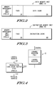
- FIG. 2 illustrates a data memory unit (DMU) circuit 32 of FIG. 1.
- DMU 32 includes a memory management unit (MMU) circuit 52, a tags circuit 54, and a data cache circuit 56.
- FIG. 3 illustrates an instruction memory unit (IMU) circuit 40 of FIG. 1.
- IMU 40 includes a memory management unit (MMU) circuit 62, a tags circuit 64, and an instruction cache circuit 66.
- FIG. 4 illustrates a portion of memory management unit (MMU) 52 of FIG. 2. Note that in one embodiment of the present invention, the portion of MMU 52 which is illustrated in FIG. 4 is identical to a portion of memory management unit (MMU) 62 of FIG. 3. In other embodiments of the present invention, FIG. 4 may illustrate a portion of only one memory management unit, or an identical portion of more than one memory management unit.
- MMU memory management unit
- Translation-Lookaside Buffer (TLB) 70 receives a logical address 80 from the data unit 30 of FIG. 1 or instruction unit 36 of FIG. 1. TLB also receives control signals from control register 74 of the control register file 72. A logical address transferred via bus 80 is typically a subset of the address bits from the data unit 30, but could be a whole address from the data unit 30. The TLB 70 then uses the logical address transferred via bus 80 to generate a physical address 100.
- TLB Translation-Lookaside Buffer
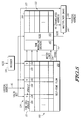
- FIG. 5 illustrates an architecture of the mapping function of a content addressable memory (CAM) array 120 and a RAM array 122 which are implemented in the TLB 70 of FIG.4 in accordance with one embodiment of the present invention.
- the mapping function enables translation between the logical address 80 and physical address 100.
- Each row 121 of the array 120 is partitioned into multiple column parings 124.
- Each pairing comprises a CAM cell group 126 which includes one or more CAM cell bits 200 of FIG. 6 and a valid bit 128. Similar pairings include CAM cell group 134 and valid bit 130 and CAM cell group 135 and valid bit 132.
- each CAM cell group 126 includes a plurality of CAM cell bits such as CAM cell bit 200 illustrated in FIG. 6.
- FIG. 5 includes three pairings per row of CAM array 120 and, therefore, can support three page sizes.
- the CAM array 120 can be partitioned into any multiple of CAM cell group 126 and valid bit 128 pairings.
- the CAM cell groups 126, 134, and 135 are shown in FIG. 5 to be roughly equivalent in size, in other embodiments of the invention a number of CAM cell bits (not shown) in each CAM cells group 126 can differ from pairing to pairing, but are constant within each pairing for all of the rows 121 except possibly a last row 150 of the CAM array.
- bits of CAM cell group (not shown in detail) to the right are more significant and the bits to the left are less significant.
- the page size translated to a physical address 100 is determined by a portion of the logical address transferred via 80 which is matched to the address stored in the CAM cell groups 126, 134, and 135 in each row 121 of the CAM array 120.
- the portion of the logical address 80 is compared to or matched with an address stored in the CAM cell groups 126, 134, and 135 is determined by the status of the valid bits 128, 130 and 132 in a row of CAM array 120. If the valid bit 128 in a CAM cell pairing 124 is asserted, then the address bits stored in that CAM cell group 126 will be matched to the portion of the logical address transferred via bus 80 corresponding to that CAM cell group.
- the second valid bit when a first valid bit to the left of a second valid bit is asserted, the second valid bit is also asserted. For example if valid bit 128 is asserted then valid bits 130 and 132 must also be asserted. Likewise, if valid bit 130 is asserted, then valid bit 132 must be asserted. Embodiments employing other configurations may also be possible.
- Decoder 136 receives page size information from the control register 74 of the control register file 72. Decoder 136 also provides page size data information to a page size register 160, illustrated as a column of the RAM array 122 in FIG. 5 .
- the last row 150 of the CAM array 120 performs a self-timing or delay function.
- Last row 150 provides an enable signal 152 to a plurality of wordline drivers 162 of RAM array 122. The enable signal enables the plurality of wordline drivers 162 to read the information provided by the plurality of s match lines 154 of the CAM array 120.
- each row 121 in the CAM array 120 represents one logical address and is connected via one of the plurality of match lines 154 to a corresponding row 123 in the RAM array 122.
- the logical address transferred via bus 80 which is to be translated is compared to the possible logical addresses in each row of CAM array 120 in order to obtain a match. If a match is found, a one of the plurality of the match lines 154 corresponding to row 121 is asserted and all non-matched row match lines 154 are not asserted.
- the self time row 150 then provides an enable signal 152 which indicates that the matching function is complete in all of the CAM array rows 121. If one of the plurality of match lines 154 and the enable signal 152 are both asserted, then one of the plurality RAM array wordline drivers 162 will select the appropriate row in the RAM array 122.
- FIG. 7 and FIG. 6 and the description provided in the following description explain how the CAM array 120 matches the logical address provided via bus 80 with possible logical addresses stored in the CAM array 120.
- each row 121 in the CAM array 120 includes a plurality of CAM cell bits and valid bits.
- FIG. 6 illustrates a CAM cell bit circuit 200 which is used to compare a bit of the input logical address provided by bus 80 and a stored possible logical address.
- FIG. 7 illustrates a valid bit circuit 128 which is used to determine whether the CAM cell bits to its left should be accessed during the matching function.
- Both CAM cell bits and valid bits include a static memory cell 202 and 252, respectively.
- the embodiments illustrated in FIGs. 6 and 7 contain six transistor static RAM memory cells (6T SRAM).
- 6T SRAM transistor static RAM memory cells
- a person reasonably skilled in the art will recognize components 204, 206, 208 and 210 in FIG. 6 and 254, 256, 258 and 260 in FIG. 7 as the 6T SRAM memory cells. It should be noted that other embodiments are possible.
- These memory cells 202 and 252 store the bits of possible logical addresses and valid bit values against which the input logical address transferred via bus 80 will be matched.
- the CAM bit circuit 200 also includes circuitry 212 for performing a logical EXCLUSIVE-OR between the value stored in the memory cell 202 and the logic address bit value on bit line, b, 214 and inverted bit line, b ⁇ , 216.
- the match line 220 is asserted.
- Match line 220 forms a portion of one of the plurality of match lines 154 of FIG. 5. If the EXCLUSIVE-OR circuitry 212 indicates a match between the value on the bit lines 214 and 216 and the value stored in memory cell 202, then transistor 222 will not be conductive and the match line 220 remains asserted. However, if EXCLUSIVE-OR circuitry 212 finds a mis-match, then transistor 222 will be conductive and the match line 220 will be pulled to a non-asserted state using the vgnd 224 line value. The vgnd 224 line value is pulled to a reference ground value using transistor 268 in valid bit 128 of FIG. 7.
- Transistor 262 is capable of isolating the portion of the match line 220 to the left of the valid bit 128 if the valid bit 128 is not asserted (in this case, a logic low value or a "0"). In this way, the valid bit 128 controls a portion of the CAM array row 121 (illustrated in FIG.
- NAND gate 264 If the valid bit 128 is not asserted, then an output of NAND gate 264 will be asserted regardless of the value on the p input line 266. When the output of NAND gate 264 is asserted, transistor 268 is conductive and enables the vgnd signal 224 to be pulled to the reference ground voltage. Referring to FIG. 6 , if there is no match between the value stored in CAM bit memory cell 202 of CAM cell bit 200 and the bit line, b, 214 value, then the "don t care" region of the match line 220 will be pulled to the reference ground voltage via the vgnd signal 224.
- the output NAND gate 264 will be determined by the p input line 266 value.
- the match line 220 is precharged to a supply voltage, Vdd, through transistor 270 while transistor 268 remains non-conductive.
- Transistor 270 also precharges the vgnd signal 224 through transistor 222 of CAM bit cell 200 illustrated in FIG. 6 to Vdd - Vt.
- Vt is the threshold voltage of the n-channel transistors.
- Match line 220 is also pulled to a logical low value through transistor 222 if a mismatch is determined in CAM bit 200.
- the match line to the right of valid bit 128 is then pulled to a logic low value using transistor 262. If a match occurs, match line 220 does not get pulled to a logic low value through transistor 222 of each of the plurality of CAM cells bits 200 to the left of an asserted valid bit. If one of the plurality of the match lines 154 is not pulled to the reference ground voltage for all the plurality of valid bits in CAM array 120, the one of the plurality of match lines 154 corresponding to a row of the CAM array 120 remains asserted to indicate a match of the logical address transferred via bus 80 occurs.
- any of the CAM cell bits 200 pulls one of the plurality of match lines 154 to a logic low value, a corresponding one of the plurality of match lines 154 will be pulled to a logic low value if the CAM bit 200 is controlled by an asserted valid bit 128 in which transistor 262 (of FIG. 6 ) is conductive. Even when one CAM cell bit pulls a match line low, a global mismatch for that row 121 of the CAM array 120 occurs.
- the match line 220 in the circuit shown in FIGs. 6 and 7 may be precharged to VDD-VT to limit the amount of power consumed due to logic level transitions involving the match lines.
- the CAM cell bit 200 also has power consumption advantages over prior art CAM cells which required the bit lines, b and b ⁇ , to vary between VDD and ground before each match operation while the match line is being precharged. Matching in CAM cell bit 200 is controlled by the vgnd 224 signal such that bit line transitions between VDD-VT and ground. Therefore, less power is consumed. In addition to smaller voltage swings, less power will be consumed because there is less loading on the vgnd signal 224 than on the data lines of prior art CAM cell bits. Power consumption savings are also gained by CAM cell bit 200 because the logical address bits supplied to the CAM array 120 are unlikely to change; therefore, bit lines 214 and 216 consume very little power consumption since they are statically driven into CAM cell bit 200.
- match lines 220 in "don't care" regions/ranges of a CAM array row 121 do not contribute to the power consumption or loading on the active portion of the match line 220. Therefore, translating addresses for page sizes which result from the assertion of fewer valid bits consume less power than page sizes which assert a larger number of valid bits.
- the translated address is transferred via bus 90 to multiplexer (MUX) 140 of FIG. 5 .
- Page size data from the page size register 160 of the RAM array 122 and the logical address transferred via bus 80 which has been matched to the translated address provided by bus 90.
- the RAM array 122 may also contain attribute bits 164 concerning attributes of the memory saved in a particular physical location. The information in the attribute bits corresponds to a particular translated address may also be sent to the MUX 140.
- FIG. 5 shows separate columns for size attribute and translated address sections, the order of this information in a row 123 in the RAM array is not important as long as the distribution of this information in the array is consistent from row to row. Additionally, although FIG. 5 shows that the size data is transferred directly to the MUX 140, it is possible that some embodiments of the invention may include an additional decoder for the size data before it is received by the MUX 140.
- FIG. 8 through FIG. 11 illustrate three examples of components of the physical address 100 output by MUX 140. They should be reviewed in conjunction with the elements illustrated on the right side of FIG. 5 . Each example contains different mixes of a translated address value 300 , and logical address components. Once again the most significant bits of data are on the right and the least significant bits are on the left. The mix of logical address components 302 and translated address components 300 is determined by MUX 140 of FIG. 5 . How much of the physical address 100 is composed of the logical address transferred via bus 80 passing through MUX 140 and how much of the physical address 100 is composed of the translated address transferred via bus 90 is determined by the page size stored in the page size register 160 in the RAM array 122. FIG. 8 through FIG.
- FIG. 11 illustrate four different possible page sizes of the present embodiment of the invention. If the page size is large, then more of the logical address is copied into the physical address. For example, see FIG. 10 .
- FIG. 11 illustrates the result of an identity operation when the entire logical address is passed to the physical address. If the page size is small then less of the logical address is copied into the physical address. For example, see FIG. 8 .
- asserted and “non-asserted” are used when referring to the rendering of a signal, status bit, or similar apparatus into its logically true or logically false state, respectively. If the logically true state is a logic level one, the logically false state will be a logic level zero. And if the logically true state is a logic level zero, the logically false state will be a logic level one. Although circuits shown may imply a certain polarity or value, this implication applies only to the preferred embodiment of the invention and not all possible embodiments of the invention.
Landscapes
- Engineering & Computer Science (AREA)
- Theoretical Computer Science (AREA)
- Physics & Mathematics (AREA)
- General Engineering & Computer Science (AREA)
- General Physics & Mathematics (AREA)
- Memory System Of A Hierarchy Structure (AREA)
Applications Claiming Priority (2)
| Application Number | Priority Date | Filing Date | Title |
|---|---|---|---|
| US38271995A | 1995-02-02 | 1995-02-02 | |
| US382719 | 1995-02-02 |
Publications (1)
| Publication Number | Publication Date |
|---|---|
| EP0725348A1 true EP0725348A1 (de) | 1996-08-07 |
Family
ID=23510119
Family Applications (1)
| Application Number | Title | Priority Date | Filing Date |
|---|---|---|---|
| EP96101054A Withdrawn EP0725348A1 (de) | 1995-02-02 | 1996-01-25 | Datenprozessor mit Nachschlagpuffer und Verfahren dafür |
Country Status (3)
| Country | Link |
|---|---|
| EP (1) | EP0725348A1 (de) |
| JP (1) | JPH08249233A (de) |
| KR (1) | KR960032174A (de) |
Cited By (2)
| Publication number | Priority date | Publication date | Assignee | Title |
|---|---|---|---|---|
| GB2365167A (en) * | 1999-12-17 | 2002-02-13 | Hewlett Packard Co | Virtual address aliasing architecture |
| EP1241579A3 (de) * | 2001-03-16 | 2004-01-21 | Fujitsu Limited | Dynamische Übersetzung von Adressen mit variabler Seitengrösse |
Citations (4)
| Publication number | Priority date | Publication date | Assignee | Title |
|---|---|---|---|---|
| EP0508577A1 (de) * | 1991-03-13 | 1992-10-14 | International Business Machines Corporation | Adressübersetzungseinrichtung |
| US5327372A (en) * | 1992-01-17 | 1994-07-05 | Matsushita Electric Industrial Co., Ltd. | Semiconductor memory device |
| EP0613089A1 (de) * | 1993-02-19 | 1994-08-31 | Digital Equipment Corporation | Inhaltsadressierbarer Speicher mit Speicherzellen zur Speicherung von gleichgültigen Zuständen für Adressübersetzung |
| GB2278211A (en) * | 1993-05-04 | 1994-11-23 | Motorola Inc | Memory management system |
-
1996
- 1996-01-18 KR KR1019960000956A patent/KR960032174A/ko not_active Withdrawn
- 1996-01-24 JP JP8029883A patent/JPH08249233A/ja active Pending
- 1996-01-25 EP EP96101054A patent/EP0725348A1/de not_active Withdrawn
Patent Citations (4)
| Publication number | Priority date | Publication date | Assignee | Title |
|---|---|---|---|---|
| EP0508577A1 (de) * | 1991-03-13 | 1992-10-14 | International Business Machines Corporation | Adressübersetzungseinrichtung |
| US5327372A (en) * | 1992-01-17 | 1994-07-05 | Matsushita Electric Industrial Co., Ltd. | Semiconductor memory device |
| EP0613089A1 (de) * | 1993-02-19 | 1994-08-31 | Digital Equipment Corporation | Inhaltsadressierbarer Speicher mit Speicherzellen zur Speicherung von gleichgültigen Zuständen für Adressübersetzung |
| GB2278211A (en) * | 1993-05-04 | 1994-11-23 | Motorola Inc | Memory management system |
Cited By (4)
| Publication number | Priority date | Publication date | Assignee | Title |
|---|---|---|---|---|
| GB2365167A (en) * | 1999-12-17 | 2002-02-13 | Hewlett Packard Co | Virtual address aliasing architecture |
| US6493812B1 (en) | 1999-12-17 | 2002-12-10 | Hewlett-Packard Company | Apparatus and method for virtual address aliasing and multiple page size support in a computer system having a prevalidated cache |
| GB2365167B (en) * | 1999-12-17 | 2004-09-22 | Hewlett Packard Co | Apparatus and method for virtual address aliasing and multiple page size support in a computer system having a prevalidated cache |
| EP1241579A3 (de) * | 2001-03-16 | 2004-01-21 | Fujitsu Limited | Dynamische Übersetzung von Adressen mit variabler Seitengrösse |
Also Published As
| Publication number | Publication date |
|---|---|
| KR960032174A (ko) | 1996-09-17 |
| JPH08249233A (ja) | 1996-09-27 |
Similar Documents
| Publication | Publication Date | Title |
|---|---|---|
| US5717885A (en) | TLB organization with variable page size mapping and victim-caching | |
| US5412787A (en) | Two-level TLB having the second level TLB implemented in cache tag RAMs | |
| US5491806A (en) | Optimized translation lookaside buffer slice having stored mask bits | |
| EP0507209A2 (de) | Datenprozessor mit gleichzeitiger statischer und dynamischer, selbständiger Markierung von Operandeninformation | |
| US5752260A (en) | High-speed, multiple-port, interleaved cache with arbitration of multiple access addresses | |
| US5519664A (en) | Dynamic random access memory persistent page implemented as processor register sets | |
| US6135651A (en) | Patching apparatus and method for upgrading modem software code | |
| US5239642A (en) | Data processor with shared control and drive circuitry for both breakpoint and content addressable storage devices | |
| US4803621A (en) | Memory access system | |
| US4158227A (en) | Paged memory mapping with elimination of recurrent decoding | |
| US5267210A (en) | SRAM with flash clear for selectable I/OS | |
| US5341500A (en) | Data processor with combined static and dynamic masking of operand for breakpoint operation | |
| EP0690386A1 (de) | Adressübersetzer und Verfahren zu seinem Betrieb | |
| EP0549321A2 (de) | Verfahren und Einrichtung zur Übersetzung von virtuellen in physikalische Adressen und zum Vergleich von Cachespeichermarken mit hoher Geschwindigkeit | |
| US5530824A (en) | Address translation circuit | |
| EP0777233A1 (de) | Speicherarchitektur mit erhaltener Adressierung und diese verwendende Systeme und Verfahren | |
| JP4445081B2 (ja) | キャッシュ・メモリ | |
| US5535351A (en) | Address translator with by-pass circuit and method of operation | |
| US5638315A (en) | Content addressable memory for a data processing system | |
| EP0549218B1 (de) | Speichereinrichtung und Verfahren zur Verwendung in einer Datenverarbeitungsanordnung | |
| US5732405A (en) | Method and apparatus for performing a cache operation in a data processing system | |
| HK1003851B (en) | A memory apparatus and method for use in a data processing system | |
| US6032241A (en) | Fast RAM for use in an address translation circuit and method of operation | |
| US6643742B1 (en) | Method and system for efficient cache memory updating with a least recently used (LRU) protocol | |
| EP0725348A1 (de) | Datenprozessor mit Nachschlagpuffer und Verfahren dafür |
Legal Events
| Date | Code | Title | Description |
|---|---|---|---|
| PUAI | Public reference made under article 153(3) epc to a published international application that has entered the european phase |
Free format text: ORIGINAL CODE: 0009012 |
|
| AK | Designated contracting states |
Kind code of ref document: A1 Designated state(s): DE FR GB |
|
| 17P | Request for examination filed |
Effective date: 19970207 |
|
| STAA | Information on the status of an ep patent application or granted ep patent |
Free format text: STATUS: THE APPLICATION HAS BEEN WITHDRAWN |
|
| 18W | Application withdrawn |
Withdrawal date: 19981130 |