EP0721286A2 - Video signal decoding apparatus with artifact reduction - Google Patents
Video signal decoding apparatus with artifact reduction Download PDFInfo
- Publication number
- EP0721286A2 EP0721286A2 EP96100033A EP96100033A EP0721286A2 EP 0721286 A2 EP0721286 A2 EP 0721286A2 EP 96100033 A EP96100033 A EP 96100033A EP 96100033 A EP96100033 A EP 96100033A EP 0721286 A2 EP0721286 A2 EP 0721286A2
- Authority
- EP
- European Patent Office
- Prior art keywords
- block
- edge
- video signal
- pixel
- decoded
- Prior art date
- Legal status (The legal status is an assumption and is not a legal conclusion. Google has not performed a legal analysis and makes no representation as to the accuracy of the status listed.)
- Withdrawn
Links
- 230000003044 adaptive effect Effects 0.000 claims abstract description 26
- 230000015654 memory Effects 0.000 claims description 50
- 238000001514 detection method Methods 0.000 claims description 30
- 238000013139 quantization Methods 0.000 claims description 11
- 238000003708 edge detection Methods 0.000 claims description 10
- 238000012935 Averaging Methods 0.000 claims description 6
- 230000001131 transforming effect Effects 0.000 claims description 6
- 238000001914 filtration Methods 0.000 claims description 4
- 230000002123 temporal effect Effects 0.000 claims description 2
- 238000000638 solvent extraction Methods 0.000 claims 3
- 238000000034 method Methods 0.000 description 62
- 230000003111 delayed effect Effects 0.000 description 25
- 230000008569 process Effects 0.000 description 20
- 230000000694 effects Effects 0.000 description 19
- 238000007906 compression Methods 0.000 description 18
- 230000006835 compression Effects 0.000 description 17
- 238000010586 diagram Methods 0.000 description 9
- 230000000875 corresponding effect Effects 0.000 description 8
- 238000012805 post-processing Methods 0.000 description 8
- 238000009499 grossing Methods 0.000 description 7
- 238000012546 transfer Methods 0.000 description 6
- 230000009466 transformation Effects 0.000 description 6
- 239000011159 matrix material Substances 0.000 description 5
- 230000008859 change Effects 0.000 description 4
- 238000005056 compaction Methods 0.000 description 4
- 230000006870 function Effects 0.000 description 4
- 230000004044 response Effects 0.000 description 4
- 230000015556 catabolic process Effects 0.000 description 3
- 238000010276 construction Methods 0.000 description 3
- 238000006731 degradation reaction Methods 0.000 description 3
- 238000004364 calculation method Methods 0.000 description 2
- 230000002596 correlated effect Effects 0.000 description 2
- 238000002372 labelling Methods 0.000 description 2
- 238000012986 modification Methods 0.000 description 2
- 230000004048 modification Effects 0.000 description 2
- 238000012545 processing Methods 0.000 description 2
- 230000002441 reversible effect Effects 0.000 description 2
- XUIMIQQOPSSXEZ-UHFFFAOYSA-N Silicon Chemical compound [Si] XUIMIQQOPSSXEZ-UHFFFAOYSA-N 0.000 description 1
- 230000005540 biological transmission Effects 0.000 description 1
- 230000006837 decompression Effects 0.000 description 1
- 238000013461 design Methods 0.000 description 1
- 230000006872 improvement Effects 0.000 description 1
- 230000007794 irritation Effects 0.000 description 1
- 230000008520 organization Effects 0.000 description 1
- 238000005192 partition Methods 0.000 description 1
- 238000011084 recovery Methods 0.000 description 1
- 229910052710 silicon Inorganic materials 0.000 description 1
- 239000010703 silicon Substances 0.000 description 1
- 230000001360 synchronised effect Effects 0.000 description 1
Images


Classifications
-
- H—ELECTRICITY
- H04—ELECTRIC COMMUNICATION TECHNIQUE
- H04N—PICTORIAL COMMUNICATION, e.g. TELEVISION
- H04N19/00—Methods or arrangements for coding, decoding, compressing or decompressing digital video signals
- H04N19/85—Methods or arrangements for coding, decoding, compressing or decompressing digital video signals using pre-processing or post-processing specially adapted for video compression
- H04N19/86—Methods or arrangements for coding, decoding, compressing or decompressing digital video signals using pre-processing or post-processing specially adapted for video compression involving reduction of coding artifacts, e.g. of blockiness
-
- H—ELECTRICITY
- H04—ELECTRIC COMMUNICATION TECHNIQUE
- H04N—PICTORIAL COMMUNICATION, e.g. TELEVISION
- H04N19/00—Methods or arrangements for coding, decoding, compressing or decompressing digital video signals
- H04N19/85—Methods or arrangements for coding, decoding, compressing or decompressing digital video signals using pre-processing or post-processing specially adapted for video compression
Definitions
- the present invention relates to a video signal that have been coded using transform coding technique and, more particularly, to a video signal decoding apparatus which can remove the ringing noise component included in that coded video signal for improved picture quality.
- the present invention further relates to a video signal decoding apparatus for removing ringing noise components around the high frequency areas of the decoded digital data and, more particularly, to a ringing noise removing apparatus especially suitable for removing ringing digital video data that are reconstructed from decompressed video data. Therefore, there is little or no degradation in quality in other areas of the reconstructed digital video that had been processed by the apparatus mentioned above, resulting in a visually more pleasant and noise reduced output.
- transform coding One of the popular form of compression is to apply transform coding to the digital signal to transform the digital signal from the spatial domain to another domain (for example the frequency domain).
- transform coding is to make used of the energy compaction property of the transformation to decorrelate the image pixel so that redundancy in the image can be removed more efficiently in the transformed domain.
- DCT Discrete Cosine Transform
- the image are divided into square blocks of pixel (says 8 x 8 pixel block) and each of these blocks is then transformed using DCT into the transformed block (8 x 8 also) which contains the DCT coefficients.
- DCT digital tomography
- the neighboring pixel in an images are in general highly correlated, this enables DCT to transform image pixel into DCT coefficients that are energy concentrated in only a few of the coefficients around the top-left corner of the transformed block, which is the low frequency region.
- These transformed blocks are then quantified into quantized coefficient and then run-length and variable length coded to further reduce the statistical redundancy present into the run-length coded data.
- the energy compaction property of DCT can be easily applied in lock of pixel that are highly correlated.
- edge block i.e. block which contains parts of edges that have sharp change in intensity across the edge, the compaction of signal energy cannot be achieved efficiently.
- FIGs. 7A, 7B, 8A, and 8B the effect of applying DCT to blocks of pixel of different natures is described later.
- Figs. 7A and 7B one example of a non edge block (8 x 8 pixel) and its corresponding transformed block are shown, respectively.
- the energy is concentrated on the top-left corner of the 8 x 8 pixel block as a result of transformation. Quantization, run-length coding and variable length coding of this transform block will produce little bits, and hence an efficient compression can be achieved.
- FIGs. 8A and 8B one example of an edge block (8 x 8 pixel) and its corresponding transformed block are shown, respectively.
- the transformed edge block (Fig. 8A) has DCT coefficients that are much more randomly distributed, when compared with the edged block.
- Such transform block is more difficult to quantized, run-length coded and variable length coded and hence the compression of the edge block cannot be done efficiently.
- the Quantization parameters are designed to preserve the low frequency coefficients at the upper left corner of the block of 8 x 8 pixel, this design will cause more error to be generated for edge block when the edge block is decoded by the decoder.
- the error will cause a ringing effect (corona effect) appearing around the edge of the reconstructed block.
- This effect causes noise component in the high frequency area of the decoded video signal, and such noise is referred to as a "ringing noise".
- FIGs. 9A, 9B, 10A, and 10B With reference to Figs. 9A, 9B, 10A, and 10B, the ringing effect are described specifically.
- This ideal vertical edge block is Discrete Cosine Transformed (DCTed), quantized, and then inverse quantized, inverse DCTed to produce the decoded block.
- DCTed Discrete Cosine Transformed
- Figs. 10A and 10B thus decoded block and its corresponding wave form are shown, respectively. It can be seen that ripples R appear on both side, enclosed by circles, of the edge constituting the ringing effects. As edge information is very sensitive to the human eyes compared to other high frequency pixel region, distortion around the edges, i.e. the ringing noise, represents a source of irritation to the viewers.
- DCT has been found to be effective for the compression of digital images.
- the block of pixel contains edge which has sharp change in intensity, the energy compaction property of DCT is no longer valid. This will result in the decoded edge block with ringing effect around the edges in the block. Such distortion is annoying to the viewers as edge provides important information to the viewers.
- Such ringing effect can be removed by performing smoothing operation to the decoded block using smoothing filter.
- smoothing filter like the average filter and median filter, also remove the contrast of the edges, thus creating a blurring effect to the originally sharp edge.
- these smoothing filters are not suitable for the removal of ringing effect.
- an edge detection algorithm needs to be designed to differentiate between an edge block from a non edge block.
- Most of the currently available edge detection algorithm involves many mathematical computation, for example, the use of squaring function, square root function or the use of surrounding blocks to help make decision. This increases the hardware complexity necessary to implement an edge enhancement filter.
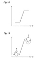
- Figs. 18 and 19 examples of frequency response of high frequency areas of digital video data before compression and after reconstruction are shown, respectively. As best shown in Fig. 19, ringing noises are observed near the high frequency area of the data reconstructed from the compressed state.
- IIR Infinite Impulse Response
- FIR Finite Impulse Response
- An apparatus had been invented which will remove the ringing noise around the high frequency areas from the reconstructed digital video while at the same time preserving the high frequency details, thus avoiding degradation in video quality.
- the said apparatus is also simple in implementation and therefore, results only in small increase in cost when adding the said apparatus as part of a postprocessing module to the decompression system for the reconstruction of digital video data from compressed data.
- the aim of this invention is to provide a very simple, and yet efficient method of removing the ringing effect around the edges in the decoded block. This method is suitable for hardware and application specific silicon chip implementation.
- the object of the present invention is therefore to provide a video signal decoding apparatus which solves these problems.
- a video signal decoding apparatus for decoding a coded video signal produced by encoding an input video signal, said apparatus comprises a variable length and run-length decoding means for decoding said coded bit to reconstruct said blocks of quantized coefficients; an inverse quantization means for inverse quantizing said blocks of reconstructed quantized coefficients; an inverse coding means for transforming said inverse quantized blocks of reconstructed quantized coefficients to produce a decoded block; an edge block detection means for determining whether said decoded block is classified as an edge block or not; and an adaptive edge enhancement filter means for removing the distortion from said decoded block when said decoded block is determined as an edge block by said block edge detection means.
- a video signal decoding apparatus Before describing a video signal decoding apparatus according to the present invention, an encoding of a digital video signal indicating images, by compressing thereof, into a bit stream is described first.
- a video signal encoder Ev for compressing a digital video signal Sv into an encoded video signal Sc that is bit streams of compressed video signal Sv is shown. Note that the video signal decoding apparatus of the present invention is used for decoding that encoded video signal Sc, and applies the post-processing thereto to enhance the decoded images.
- the video signal encoder Ev includes a frame memory 131, a block sampler 102, a motion vector estimator 103, a motion compensator 104, a discrete cosine transformer 105 which is indicated as "DCT”, a quantizer 106, a rate controller 107, a coding unit 108, an inverse quantizer 109, an inverse discrete cosine transformer 110 which is indicated as "inverse DCT", a local decoded frame memory 111, and a reference frame memory 112, connected to each other as best shown in Fig. 5.
- the video signal encoder Ev utilizes a DCT and motion estimation and compensation technique.
- An input digital interlaced video sequence Sv first enters the frame memory 131 in a frame by frame basis.
- the input video frames are classified into predictive frame (P-frame) or intra frame (I-frame).
- the I-frame is coded independently of the other frames, i.e. it is compressed without the use of any other frame.
- the I-frame is used periodically to allow for easy random access, fast forward/reverse and easy error recovery.
- the P-frame is coded with motion estimation and compensation using previously coded frame to predict the contents of the current frame to be coded.
- Motion estimation and compensation is used to reduce the temporal redundancy in the digital video sequences and thereby increase the compression ratio.
- an input digital frame Sv When an input digital frame Sv is fed into the frame memory 131, it is also passed to the reference frame memory 112 for the motion estimation process thereby. It is then passed to a block sampler 102.
- the block sampler 102 partitions the image into spatially non-overlapping blocks of pixel data. To provide a reasonable level of adaptiveness, a block size of 8 x 8 pixel may be used.
- the sampled blocks are then transferred to DCT 105 when a well known transform coding method, Discrete Cosine Transform (DCT), is performed.
- DCT Discrete Cosine Transform
- the pixel data is transformed to obtain block of DCT coefficients.
- DCT coefficients are then transferred to the quantizer 106.
- the quantizer 106 produces the quantized coefficients.
- the Quantizer 106 uses a quantizer matrix and quantizer step size given by the rate controller 107.
- the rate controller 107 ensures that a fairly constant amount of data is generated per second.
- the quantized coefficients are then transferred to the coding unit 108 which performs a routine of the run-length coding and variable length coding of the quantized coefficients.
- the result of the Run-length Coding & Variable Length Coding by the coding unit 108 is the output as bit stream that is the video signal Sc bit stream to be stored or transmitted to the receiver.
- the coding unit 108 also transfers this bit stream to the rate controller 107.
- the quantizer 106 also transfers the quantized coefficients to the inverse quantizer 109 which performs the reverse of quantization to obtain the inverse-quantization coefficients. These inverse-quantization coefficients are then transferred to Inverse DCT 110 for the inverse DCT process to obtain the inverse DCT coefficients. The inverse DCT coefficients are also the decoded pixel block. The decoded pixel block are then transferred to the local decoded frame memory 111 to form the reconstructed (also referred to as "decoded") frame. The reconstructed frame will be used by the motion compensator 104 to process for the pixel block of the P-frame.
- the block of pixel data (block to be coded) from the block sampler 102 is transferred not to the DCT 105 but to the motion vector estimator 103.
- the estimator 103 estimates the motion vector by finding the best matched block from the pixel data of a pervious frame. The horizontal and vertical offset of the best matched block from the previous frame, which together from the motion vector, are obtained. The block of pixel data and its corresponding motion vector are then transferred to the motion compensator 104.
- the motion compensator 104 obtains blocks of data (referred to as "predicted block") from the previously reconstructed frame based on the decoded frame output from the local decoded frame memory 111, by using the offset given by the motion vector. Differences between values of the block to be coded and the predicted block are computed to obtain a differential block composed of the different values.
- the block When the energy (for example, calculating the standard deviation of the block) of this difference block is smaller than the energy of the block to be coded, the block will then be coded with motion compensation. Otherwise, the block to be coded will be coded as it is.
- An information bit will be used to indicate whether the motion compensation is done to the block, or not.
- this difference block is then transferred to the DCT 105 for the Discrete Cosine Transformation (DCT). Otherwise, the block to be coded will be transferred to the DCT 105.
- the other process are the same as the case of I-frame.
- the motion vector is also transferred as a side information, to the DCT 105, to Quantization 6, and to the coding unit 108, and is then multiplexed with the variable length coded information of the difference block.
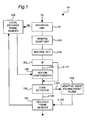
- the video signal decoding apparatus Dv includes a decoding unit 141, an inverse quantizer 143, an inverse discrete cosine transformer 145 indicated as "inverse DCT”, a switch 153 indicated as "SI”, a motion compensator 149, an edge detector 158, an adaptive edge enhancement filter 162, a decoded frame memory 151, and a local decoded frame memory 155 indicated as "DECODED FRAME MEMORY”.
- the decoding unit 141 is connected to the coding unit 108 (Fig. 5) of the video signal encoder Ev for receiving the encoded video bit stream Sc therefrom.
- This bit stream Sc is the compressed video signal and also has a coded information.
- the decoding unit 141 applies the encoded video signal Sc with a Variable Length & Run-length Decoding operation. Then, decoding unit 141 demultiplexes and decodes the variable length codes to produce the quantized coefficients of each block of the coded frame and the side information of the block, i.e. the motion vector MV and the information bit on whether the block is motion compensated or not.
- the decoding unit 141 also checks the frame number of the frame to be decoded to see whether the frame is I-frame or P-frame.
- the inverse quantizer 143 is connected to the decoding unit 141 for receiving the decoded quantized coefficient block therefrom to apply an inverse quantization process thereto.
- the inverse DCT (inverse Discrete Cosine Transformer) 145 is connected to the inverse quantizer 143 for receiving the inverse quantized coefficient block therefrom to apply an inverse discrete cosine transformation process thereto.
- the inverse DCT 145 produces the inverse DCTed coefficient block that is a sequence of blocks of decoded pixel data.
- the switch 153 is connected to the inverse DCT 145 for receiving the inverse DCTed coefficient block therefrom, and receives the side information of the block from the decoding unit 141 through the inverse quantizer 143 and the inverse DCT 145.
- the switch 153 checks the frame number thereof to determine whether the frame to be decoded is I-frame or P-frame.
- the switch 153 has a first output port connected to the motion compensator 149 by a line L148 and a second output port connected to the edge detector 158 by a line L147.
- the switch 153 sends the output from the inverse DCT 145 directly to the edge detector 158 through the line 147 for an edge detection process which is described in detail with reference to Fig. 4 later.
- the switch 153 checks the information bit indicating whether a block is coded with motion compensation or not and. When it is indicated that the block output from the inverse DCT 145 had been coded without motion compensation by an encoder such as typically shown in Fig. 5, the switch 153 sends that block directly to the edge detector 158 through the line L147, for which an edge detection process is again done on the blocks of decoded pixel.
- the switch 153 sends that block to the motion compensator 149 through the line L148. It is because that the block of decoded pixel is the differential block and a predicted block has to be obtained with a motion compensation process performed in the motion compensator 149. In such case, the switch 153 sends the output of the inverse DCT 145 to the motion compensator 149.
- the local decoded frame memory 155 is connected to the decoding unit 141 for receiving the decoded motion vector MV to produce a predicted block using the offset given by that decoded motion vector MV.
- the motion compensator 149 is also connected to the decoded frame memory 155 for receiving the predicted block therefrom.
- the motion compensator 149 adds the difference block from the switch 153 to the predicted block from the memory 155, and produces a constructed block.
- the edge detector 158 is also connected to the motion compensator 149 for receiving the reconstructed block therefrom to apply the edge detection process thereto.
- the edge detector 158 checks whether the reconstructed block is a block containing edge information (edge block) or not (non-edge block).
- the edge detector 158 has a first output port connected to the adaptive edge enhancement filter 162 by a line L161 and a second output port connected to the decoded frame memory 151 by a line L160.
- the edge detector 158 transfers the block to the adaptive edge enhancement filter 162 through the line L161.
- the adaptive edge enhancement filter 162 performs an adaptive filtering process to remove the ringing effect and generate the filtered block. Details of the adaptive edge enhancement filter 162 will be described in later with reference to Figs. 3A and 3B.
- the detector 158 transfers the block to the decoded frame memory 151 through the line L160.
- the decoded frame memory 151 is also connected to the adaptive edge enhancement filter 162 by a line L163 for receiving the filtered block therefrom.
- the decoded frame memory 151 is further connected to the decoded frame memory 155 for outputting the data stored therein as an output reconstructed sequence therefrom. The output reconstructed sequence will be used for motion compensation of the next frame.
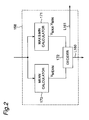
- the edge detector 158 includes a mean calculator 170, a maximum and minimum calculator 171 each connected to the motion compensator 149 and the switch 153 for receiving the decoded block therefrom, as described in the above.
- the mean calculator 170 calculates the mean value V MEAN of the block
- the maximum and minimum calculator 171 calculates the maximum value V MAX and the minimum value V MIN of the decoded block.
- the edge detector 158 further includes a decider 172 connected to both the mean calculator 170 and the maximum and minimum calculator 171 for receiving the calculated values V MEAN , V MAX , and V MIN therefrom.
- the decider 172 obtains a first absolute difference Da1 between the maximum value V MAX and the mean value V MEAN and a second absolute difference Da2 between the minimum value V MIN and the mean value V MEAN .
- the decider 172 compares thus obtained absolute differences Da1 and Da2 with a first threshold Th1 that is a predetermined value suitable for determining the block to be smoothed, and is chosen to "48" in this embodiment.
- a first threshold Th1 that is a predetermined value suitable for determining the block to be smoothed, and is chosen to "48" in this embodiment.
- the decider 172 judges that the decoded block is an edge block. Otherwise, the decider 172 judges the decoded block as a non-edge block. According to this judgment, the decider 172 selectively transfers the decoded blocks either of the adaptive edge enhancement filter 162 and the decoded frame memory 151, as described in the above.
- Figs. 3A and 3B the pixel labelling performed by the adaptive edge enhancement filter 162 of Fig. 1 are described briefly.
- Fig. 3A the blocks of pixel on the left is the 8 x 8 decoded block which has been classified as an edge block is shown.
- Fig. 3B the post-processed block of the edge block of Fig. 3A is shown.
- the adaptive filter is applied to the pixel values of the decoded block one at a time, starting from the top-left corner, going horizontally and ending at the bottom-right corner.
- the corresponding filtered value is stored in the processed edge block of Fig. 3B.
- a pixel at the 3rd row and the 4th column of the edge block of Fig. 3A, which is represented by P0 is targeted, the adaptive filter uses its surrounding pixel (P1, P2, P3 P8) to generate a post-processed value S0 and stored in the processed edge block (Fig. 3B).
- P1, P2, P3 P8 the surrounding pixel
- each of 9 pixels having a target pixel P0 and surrounding 8 pixels can be represented by reference Pi, wherein "i" is a positive integer smaller than 9 and including 0, as shown.
- the adaptive edge enhancement filter 162 When every edge block enters into the adaptive edge enhancement filter 162, the adaptive edge enhancement routine starts, for processing the edge block on a pixel-by-pixel basis. Each pixel is adaptive filtered using the surrounding pixels.
- step S1 it is judged whether any pixel not processed is rested in the edge block or not. When all pixels in the block have been processed, it is judged as "NO”. Then the procedure terminates. However, since the newly entered block has pixels not processed, it is judged "YES”. Then, the procedure advances to step S3 for being processed.
- step S3 all of parameters "i”, "sum”, and “count” are set to 0.
- the center pixel P0 shown in Fig. 3A is set as the target pixel for the processing.
- the procedure advances to next step S5.
- step S5 it is judged whether "i" is smaller than 9 or not. When “i” is smaller than 9, it means that any of surrounding 8 pixels is still not examined. Then, it is judged as "NO" and the procedure advances to step S7.
- step S7 it is judged whether the difference between the center pixel P0 and its surrounding pixel Pi is smaller than a second threshold Th2 having a predetermined value.
- a second threshold Th2 having a predetermined value.
- step S11 the value of count is increased by 1 and the value of Pi is also added to sum. Then the procedure advances to step S9.
- step S9 "i" is incremented by 1, and then the procedure returns to step S5.
- "i" is incremented by 1, and then the procedure returns to step S5.
- step S7 when it is judged as "NO”, it means that the difference (Pi - P0) is equal to or greater than the second threshold Th2.
- the procedure also advances to step S9.
- step S9 when "i" becomes 9 as a result of addition at step S9, it is judged as "YES” at step S5. Then the procedure advances to step S13. Thus, the loop of step S5, S7, S11, and S9 is repeated until when all the surrounding eight pixels are scanned.
- step S13 it is judged whether the value of count is equal to either of 0, 1, 3, and 7, or not.
- step S19 the procedure advances to step S19.
- step S19 the count is incremented by 1, and the center pixel P0 is added to the sum. Then, the procedure advances to step S25.
- step S13 it is meant that count is equal to neither of 0, 1, 3, and 7.
- step S15 it is meant that count is equal to neither of 0, 1, 3, and 7.
- step S15 it is judged whether value of count is equal to 5 or not. When the count is equal to 5, it is judged as "YES”. Then the procedure advances to step S21.
- step S21 the count is incremented by 3.
- the three times of the center pixel P0 is added to the sum. Then the procedure advances to step S25.
- step S15 when it is judged as "NO" at step S15, the procedure advances to step S17.
- step S17 it is judged whether the value of count is equal to 6 or not.
- the procedure advances to step S23.
- step S23 the count is increased by 2 and two times of the center pixel P0 is added to the sum. Then, the procedure advances to step S25.
- step S17 it is judged as "NO" the procedure advances to step S25.
- the post-processed block S0 is calculated by taking the division of sum by count.
- the second threshold Th2 is set to be at 16, but can be chosen to any predetermined value enabling surrounding pixels on the same side of the edge to be smoothed. Then, the procedure advances to step S27.
- step S27 the post-processed block S0 is put to process edged block, and then the procedure returns to step S1 to examine the next block.
- the post-processed edge block according to the present invention and its corresponding waveform are shown, respectively.
- the post-processed block has a significantly reduced ringing effect.
- performing the smoothing function on the coded picture means that no extra information needs to be transmitted by the coder to the decoder and hence no change in the bit-syntax is needed.
- the first step in the operation is to take the decoded block from the decoder and pass it through an edge deduction circuit to determine if the decoded block contains any edge information. If edge information is present in the block, the block is classified as edge block; otherwise, it is classified as non-edge block.
- the edge block is passed through a smoothing filter circuit which performs an averaging process adaptively, using only neighboring pixel from the same side of the edge for the averaging process.
- the neighboring pixel are classified as to be on the same side of the edge as the pixel to be smoothed or on different side of the edge using a thresholding technique. If the value of neighboring pixel differs from the pixel to be smoothed by less than the threshold value, it is classified as to be on the same side of the edge as the pixel to be smoothed; otherwise, it is on the different side of the edge to be smoothed.
- the averaging process then uses only those neighboring pixel which are on the same side as the pixel to be smoothed for the calculation of the average value.
- the ringing noise removing apparatus Rn includes a video data decoder 1, a ringing noise source detector 2, a status memory 3, a recorder memory 4, a ringing noise filter 5, and a post processing unit 6.
- the video data decoder 1 is provided for receiving a compressed video data Sc from a suitable data source such as a digital video cassette recorder.
- the video data decoder 1 decompresses the compressed data Sc to reconstruct the original video data Sp.
- This reconstructed data Sp is output from the video data decoder 1 at random and at high transfer rate, and is arranged in a block format having a matrix formed by 8 x 8 pixels, for example.
- the ringing noise source detector 2 is connected to the vide data decoder 1 for receiving the video pixel data Sp therefrom to detect the ringing noise components included in the data Sp to produce a first detection level signal S DS1 and a writing command signal S W .
- the status memory 3 is connected to the ringing noise source detector 2 for receiving the signals S DS1 and S W therefrom to store the detection status of the pixel data.
- the reorder memory 4 is connected to the video data decoder 1 for receiving the pixel data Sp therefrom.
- the reorder memory 4 reorders frames of the pixel data Sp to convert thereof from the block format into a raster scan format.
- the pixel data Sp is converted into a raster scan pixel data Sr suitable for raster scanning and other decoder system's purpose.
- the ringing noise filter 5 is connected to the status memory 3 and the reorder memory 4 for receiving the signals (data) S DS2 and Sr therefrom, respectively.
- the ringing noise filter 5 filters a ringing noise components from the data Sr with respect to the signal S DS2 , and further produces the reading command signal S RD .
- the ringing noise filter 5 is further connected to the status memory 3 for feeding the signal S RD back thereto. Then, the ringing noise filter 5 outputs a ringing noise filtered data S F whose ringing noise components are removed therefrom.
- the post processor 6 is connected to the ring noise filter 5 for receiving the filtered pixel data S F to apply post-processing such as interpolation, and produces a pixel data Sp' which is the reproduction of the original pixel data.
- the detector 2 includes a First In First Out buffer memory 7, hereinafter referred to as "FIFO buffer", connected to the video data decoder 1 for receiving the reconstructed pixel data Sp therefrom.
- the FIFO buffer 7 outputs thus received pixel data Sp therefrom in the same order in which the FIFO buffer 7 received. Furthermore, the FIFO buffer 7 produces a flag signal Fs indicating whether the pixel data Sp is current present therein, or not.
- a pixel level detection controller 8 is connected to the FIFO buffer 7 for receiving the flag signal Fs to check the status of FIFO buffer 7.
- the controller 8 produces a reading signal Sr1 and the writing command signal S W when the flag signal Fs indicates that the FIFO buffer 7 current has data Sp therein.
- the pixel level detection controller 8 is also connected to the FIFO buffer 7 for transferring the reading command signal Sr1 thereto so as to outputs the reconstructed data Sp therefrom.
- a pixel level detector 50 is connected to the FIFO buffer 17 and the pixel level detection controller 8 for receiving the reconstructed data Sp and the reading command signal Sr1 therefrom, respectively.
- the pixel level detector 50 detects the pixel level of the reconstructed data Sp outputted from the FiFO buffer with respect to the reading command signal Sr1.
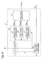
- the pixel level detector 50 includes a maximum pixel comparator 9, a mean block calculator 10, and minimum pixel comparator 11 each connected to the FIFO buffer 7 and the pixel level detection controller 8, respectively, as best shown in Fig. 12.
- the maximum pixel comparator 9 checks and compares all pixels in the reconstructed block data Sp to detect the maximum value thereof, and further produces a first level signal S MAX with respect to the reading signal Sr1.
- the reading signal Sr1 is used as a clock signal for reading operation.
- the minimum pixel comparator 11 checks and compares all pixels in the reconstructed block data Sp for the minimum value, and produces a second signal S MIN .
- the mean block calculator 10 calculates an average value of the pixels in the block Sp, and produces a third signal S MEAN . Note that the reading signal Sr1 is used as an output clock for the FIFO buffer 7 and pixel level detector 50.
- a pixel level comparator 12 is connected to the pixel level detector 50 for receiving the level signals S MAX , S MIN , and S MEAN therefrom. Base on these level signals, the pixel level comparator 12 completes the final computation to determine the detection status of the block data Sp being examined, and produces a first detection level signal S DS1 .
- the pixel level detector 12 includes a first subtracter 13, a second subtracter 14, a first comparator 15, a pixel level detection threshold setter 16, and a second comparator 17.
- the threshold setter 16 produces a threshold signal S TH having a predetermined value, or can store the threshold signal S TH supplied from an external means such as a keyboard operated by an operator.
- the first subtracter 13 is connected to the maximum pixel comparator 9 and the mean block calculator 10 of the pixel level comparator 12 for receiving the signals S MAX and S MEAN therefrom, respectively.
- the second subtracter 14 is connected to the mean block calculator 10 and the minimum pixel comparator 11 of the pixel level comparator 12 for receiving the signals S MEAN and S MIN therefrom, respectively.
- the mean value is essentially less than or equal to the maximum value, and is greater than or equal to the minimum value of the data block pixels Sp. Therefore, the first subtracter 13, subtracts the mean value signal S MEAN from the maximum value signal S MAX to produce a first difference signal Sd1. Similarly, the second subtracter 14 subtracts the minimum value signal S MIN from the mean value signal S MIN to produce a second difference signal Sd2.
- the first comparator 15 is connected to the subtracters 13 and 14 for receiving the difference signals Sd1 and Sd2, respectively, to compare thereof.
- the first comparator 15 multiplexes either one of the two difference signals Sd1 and Sd2 having a greater value to output as a comparison signal S DC therefrom.
- the comparison signal S DC is a direct current.
- the second comparator 17 is connected to the first comparator 15 and the pixel level detection threshold setter 16 for receiving the signal S DC and the threshold signal S TH therefrom, respectively.
- the comparator 17 compares the comparison signal S DC with the threshold signal S TH to produce and output the first detection level signal S DS1 therefrom.
- the first detection level signal S DS1 can be regarded as a pixel status signal indicating the status of the ringing noise in the block pixels.
- the status memory 3 is connected to both the pixel level comparator 12 and the pixel level detection controller 8 of the ringing noise detector 2 for receiving the first detection level signal S DS1 and the writing command signal S W therefrom, respectively.
- the status memory 3 stores the signal S DS1 together with the writing command signal Sw therein. The operation of the status memory 3 will be described later with respect to the ringing noise filter 5 below.
- the circuitry is synchronous and is clocked by the operation clock that is a vertical synchronization signal V. sync.
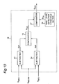
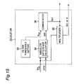
- the ringing noise filter 5 includes first and second line memories 18 and 19 each having a memory length equal to the number of pixel data in one raster scan line.
- the first line memory 18 is connected to the reorder memory 4 for receiving the raster scan pixel data Sr to delay by one line, and then produces a first delayed pixel data Sr1. This data Sr1 is delayed from the pixel data Sr by one line period.
- the second line memory 19 is connected to the first line memory 18 for receiving the first delayed pixel data Sr1 therefrom to also delay by one line, and then produces a second delayed pixel data Sr1'. This data Sr1' is delayed from the pixel data Sr by one line period.
- the first resistor 21 is connected to the reorder memory 4 for receiving the raster scan pixel data Sr to delay by one operation clock, and then produces a third delayed data Src. This data Src is delayed from the pixel data Sr by one clock period.
- the second resistor 24 is connected to the first line memory 18 for receiving the second delayed pixel data Sr1 therefrom to delay by one clock, and then produces a fourth delayed pixel data Srlc. This data Srlc is delayed from the data Sr by one line and one clock period.
- the third resistor 25 is connected to the second resistor 24 for receiving the fourth delayed pixel data Srlc therefrom to delay thereof by one clock, and then produces a fifth delayed pixel data Srlc'.
- This data Srlc' is delayed from the data pixel Sr by one line and two clocks period.
- the fourth resistor 26 is connected to the second line memory 19 for receiving the second delayed pixel data Srl' to delay thereof by one clock, and then produces a sixth delayed pixel data Srl'c.
- This data Srl'c is delayed from the data Sr by two lines and one clock period.
- the fifth delayed pixel data Srlc indicates the pixel data to be filtered and the center pixel of a filter matrix, and is referred to as "a center pixel signal CPX".
- pixels contributing to the computation of the filtering of the center pixel are one line ahead of it at the output of the fourth resistor 26, one clock ahead at the output of the third resistor 25, one clock delayed at the line memory 18 output and one line delayed at the output of DFF 21.
- the first pixel multiplexer 22 is connected to the first and second registers 21 and 24 for receiving the third delayed pixel data Src and the center pixel signal CPX (Srlc), and produces a first comparison signal Sc1.
- the pixel multiplier 22 includes a filter threshold setter 33, an absolute difference calculator 34, a multiplexer 35, and a comparator 36.
- the filter threshold setter 33 produces a threshold signal S TF having a predetermined value, or can store the threshold signal S TF supplied from an external means such as a keyboard operated by an operator.
- the absolute difference calculator 34 is connected to the first resistor 21 and the second resistor 24 for receiving the third delayed pixel data Src and the center pixel signal CPX therefrom, respectively.
- the calculator 34 calculates an absolute difference between the two data Src and CPX to produce a third difference signal Sd3.
- the comparator 36 is connected to the filter threshold setter 33 and the absolute difference calculator 34 for receiving the filter threshold signal S TF and the third difference signal Sd3 therefrom, respectively.
- the comparator 36 compares these signals S TF and Sd3 to produce the first comparison signal Sc1 having two levels “0" and "1". For example, when the absolute difference Sd3 is greater than the threshold S TF , the comparison signal Sc1 has “1" level, and otherwise "0" level.
- the multiplexer 35 is connected to the first register 21 and the comparator 36 for receiving the third delayed pixel data Src and the first comparison signal Sc1 therefrom, respectively.
- the multiplexer 35 outputs the pixel data Src.
- the multiplexer 35 outputs a zero value signal.
- a summation unit 29 is connected to the multiplexer 35 of the first pixel multiplexer 22 for receiving the signal Src or the zero value signal therefrom.
- a divisor generator 31 is connected to the comparator 36 of the first pixel multiplexer 22 for receiving the first comparison signal Sc1 therefrom.
- each of the pixel multiplexers 23, 27, and 28 has a construction identical to that of the pixel multiplexer 22, as described in the above, the operation thereof is substantially the same. Therefore, only the portions of multiplexers 23, 27, and 28 different from the first multiplexer 21 are described bellow.
- the second pixel multiplexer 23 is connected to the first line memory 18, the second register 24, the summation unit 29, and the divisor generator 31, as shown in Fig. 14. Similarly, the second pixel multiplexer 23 produces a second comparison signal Sc2, and outputs the first delayed pixel data Sr1 or the zero value signal according to the second comparison signal Sc2.
- the third pixel multiplexer 27 is connected to the second line memory 19, the second register 24, the summation unit 29, and the divisor generator 31. Similarly, the third pixel multiplexer 27 produces a third comparison signal Sc3, and outputs the sixth delayed pixel data Srl'c or the zero value signal according to the third comparison signal Sc3.
- the fourth pixel multiplexer 28 is connected to the third register 25, the second register 24, the summation unit 29, and the divisor generator 31. Similarly, the fourth pixel multiplexer 28 produces a fourth comparison signal Sc4, and outputs the fifth delayed pixel data Srlc' or the zero value signal according to the third comparison signal Sc4.
- the divisor generator 31 receives the four comparison signals Sc1, Sc2, Sc3, and Sc4 from the four pixel multipliers 22, 23, 27, and 28, respectively. Based on these four signals, the divisor generator 31 produces a divisor signal Sdv.
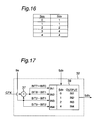
- a logic table of the divisor generator 31 is shown. Since each of comparison signals Sc1, Sc2, Sc3, and Sc4 can be "0” or “1” as described in the above, a summed value Scs of the four comparison signals Sc1, Sc2, Sc3, and Sc4 becomes either of numbers “0", “1", “2”, “3”, and “4". When the summed value Scs is “0”, the divisor generator 31 outputs "1” as the divisor Sdv. Similarly, when the summed value Scs is "1", “2", and “3 or 4", the divisor Sdv is set to "1", "2", and "4", respectively.
- the summation unit 29 receives the pixel data Src (or zero), Sr1 (or zero), Srl'c (or zero), and Srlc' (or zero) from the multipliers 22, 23, 27, and 28, respectively, and sums thereof up to produce a summation signal Ss.
- a divider 32 is connected to the summation unit 29, the divisor generator 31, and the second register 24 for receiving the summation signal Ss, the divisor signal Sdv, and the center pixel signal CPX, respectively, therefrom. Based on these three signals, the divider 32 produces a division signal Sdiv.
- the divider 32 includes an adder 37 and a dividing computer 38 connected to each other as shown.
- the adder 37 is connected to the second register 24 and the summation unit 29 for receiving the center pixel signal CPX and the summation signal Ss, respectively, therefrom to add thereof.
- the dividing computer 38 has four input ports IN1, IN2, IN3, and IN4.
- the input ports IN1 and IN2 are connected to the adder 37 for receiving the added single CPX and Ss therefrom.
- the input ports IN3 and IN4 are connected to the summation unit 29 for receiving the summation signal Ss therefrom.
- the dividing computer 38 selects one of signals that are taken therein through the input ports IN1, IN2, IN3, and IN4 based on the divisor signal Sdv, and further outputs thus selected signal therefrom as the division signal Sdiv.
- the dividing logic thereof is schematically shown.
- the divisor signal Sdv is "0"
- the signal input through the input port IN1 is selected and output as the division signal Sdiv.
- the divisor signals Sdv is "1", "2”, or "4"
- the input signals through the ports IN2, IN3, and IN4 are output, respectively, from the divider 32.
- the selected bits from either the adder 37 or the summation 29 will be output from the divider 32.
- a circular buffer controller 20 is connected to the status memory 3, and operates bases on a vertical synchronization signal V. Sync. supplied thereto.
- the circular buffer controller 20 generates a read signal S RD including the memory address and reading command so as to read the second detection level signal S DS2 from the status memory 3 as well as to keep track of the position of the pixel being filtered.
- a data multiplexer 30 is connected to the status memory 3 (Fig. 11), the second register 24, and the divider 32 for receiving the second detection level signal S DS2 , the central pixel signal CPX, and the division signal Sdiv, respectively, therefrom.
- the data multiplexer 30 multiplexes the division signal Sdiv with the central pixel data CPX by the second detection level signal S DS2 .
- the data multiplexer 30 will output the data Sdiv from the divider 32 when the detection level (or status) signal S DS2 indicates presence of ringing noise within that pixel (CPX) boundaries or else the pixel value remains unchanged from previous i.e. prior to input of the ringing noise filter 5.
- the data that is outputted by the multiplexer 30 will then be the final output of the ringing noise filter 5, and is the filtered pixel data S F .
- the ringing noise removing apparatus of the present invention is capable of maintaining the reconstructed video sharpness while removing the ringing noise effect from the reconstructed vide by detecting the sources causing such noise and applying an adaptive filter to the detected areas. Also, according to the present invention, complex mathematical calculations are not necessary, and only an independent process is required. Thus, makes it fairly easy to implement in conjunction with a video decoder (or decompressor). Hence, the apparatus of the present invention has a large effect in removal of the ringing noise form reconstructed video at low cost and complexity.
- the ringing noise removing apparatus reads in the reconstructed digital video data in a block by block basis from the decompress (or decoder). Each block is then detected for the high frequency areas which is a potential source of the ringing noise. The frequency level detected depends on the detection threshold which can be adjusted. The block detection status generated is then stored. This detection status is used for filtering control.
- the reconstructed video data is converted from block format into raster scan through the reorder memory.
- the pixel data is converted to raster scan, it is output to the ringing noise filter.
- the pixel to be filtered is assumed to be in the center of a 3 x 3 matrix. All the pixels within the matrix is then compared with an adjustable threshold. Pixels within a certain range are then selected for the computation f the filter result. Using the pixels selected, the filter result of the particular pixel is then calculated.
- the filtered pixel is then multiplexed with the original pixel using the detection status which was stored earlier. The detection status act as the control for the multiplex to produce the final output from the apparatus.
Landscapes
- Engineering & Computer Science (AREA)
- Multimedia (AREA)
- Signal Processing (AREA)
- Compression Or Coding Systems Of Tv Signals (AREA)
Abstract
Description
- The present invention relates to a video signal that have been coded using transform coding technique and, more particularly, to a video signal decoding apparatus which can remove the ringing noise component included in that coded video signal for improved picture quality.
- The present invention further relates to a video signal decoding apparatus for removing ringing noise components around the high frequency areas of the decoded digital data and, more particularly, to a ringing noise removing apparatus especially suitable for removing ringing digital video data that are reconstructed from decompressed video data. Therefore, there is little or no degradation in quality in other areas of the reconstructed digital video that had been processed by the apparatus mentioned above, resulting in a visually more pleasant and noise reduced output.
- Digital transmission and storage of video signal and its associated audio has attracted a lot of attention recently because of the superior quality and greater flexibility compared to the analog signal. However, as digital video picture requires a large amount of data for its representation, this creates a constraint on its widespread use. Coding (compression) technique were developed to reduce the amount of data needed to represent the video signal.
- Various techniques of compression have been explored for the compression of video signal. These methods are usually lossy in nature, that is, they attempt to use less amount of bits to represent the most important information present in the data, such that normal viewers of the decoded video signal will find it difficult to detect the difference between the decoded video signal and the original non-coded signal.
- One of the popular form of compression is to apply transform coding to the digital signal to transform the digital signal from the spatial domain to another domain (for example the frequency domain). The idea behind transform coding is to make used of the energy compaction property of the transformation to decorrelate the image pixel so that redundancy in the image can be removed more efficiently in the transformed domain.
- Various transformation techniques has been explored for the removal of redundancy in the spatial domain, and Discrete Cosine Transform (DCT) is found to be the best transformation from efficient and implementation complexity point of view. Thus, DCT has been the basic core technique of a few recently established International Standardization Organization (ISO) standards for the compression of images, which include JPEG (Joint Photographic Expert Group), MPEG (Moving Picture Expert Group) Phase-1, MPEG Phase-2, h.261 (CCITT standards, used mainly for teleconferencing).
- To compress an image using the DCT method, the image are divided into square blocks of pixel (says 8 x 8 pixel block) and each of these blocks is then transformed using DCT into the transformed block (8 x 8 also) which contains the DCT coefficients. As the neighboring pixel in an images are in general highly correlated, this enables DCT to transform image pixel into DCT coefficients that are energy concentrated in only a few of the coefficients around the top-left corner of the transformed block, which is the low frequency region. These transformed blocks are then quantified into quantized coefficient and then run-length and variable length coded to further reduce the statistical redundancy present into the run-length coded data.
- The energy compaction property of DCT can be easily applied in lock of pixel that are highly correlated. However, in the case of edge block, i.e. block which contains parts of edges that have sharp change in intensity across the edge, the compaction of signal energy cannot be achieved efficiently.
- With reference to Figs. 7A, 7B, 8A, and 8B, the effect of applying DCT to blocks of pixel of different natures is described later. In Figs. 7A and 7B, one example of a non edge block (8 x 8 pixel) and its corresponding transformed block are shown, respectively. As best shown in Fig. 7B, the energy is concentrated on the top-left corner of the 8 x 8 pixel block as a result of transformation. Quantization, run-length coding and variable length coding of this transform block will produce little bits, and hence an efficient compression can be achieved.
- In Figs. 8A and 8B, one example of an edge block (8 x 8 pixel) and its corresponding transformed block are shown, respectively. As best shown in Fig. 8B, the transformed edge block (Fig. 8A) has DCT coefficients that are much more randomly distributed, when compared with the edged block. Such transform block is more difficult to quantized, run-length coded and variable length coded and hence the compression of the edge block cannot be done efficiently.
- Furthermore, in order to compress more bits, the Quantization parameters are designed to preserve the low frequency coefficients at the upper left corner of the block of 8 x 8 pixel, this design will cause more error to be generated for edge block when the edge block is decoded by the decoder. The error will cause a ringing effect (corona effect) appearing around the edge of the reconstructed block. This effect causes noise component in the high frequency area of the decoded video signal, and such noise is referred to as a "ringing noise".
- With reference to Figs. 9A, 9B, 10A, and 10B, the ringing effect are described specifically. In Figs. 9A and 9B, one example of an ideal vertical edge block and its corresponding waveform are shown, respectively. This ideal vertical edge block is Discrete Cosine Transformed (DCTed), quantized, and then inverse quantized, inverse DCTed to produce the decoded block.
- In Figs. 10A and 10B, thus decoded block and its corresponding wave form are shown, respectively. It can be seen that ripples R appear on both side, enclosed by circles, of the edge constituting the ringing effects. As edge information is very sensitive to the human eyes compared to other high frequency pixel region, distortion around the edges, i.e. the ringing noise, represents a source of irritation to the viewers.
- To solve this problem, an efficient method of removing the ringing effect around the edge is disclosed in the Japanese Laid-open Patent Publication No. H6-292173 published October 18, 1994, by Siew Tan Chong and entitled and assigned to the same assignee of the present invention. In this previously disclosed method, the decoded block is subject to an edge detection process which classified the said decoded block into edge block and non-edge block, and then subjecting the edge block to adaptive smoothing process to reduce the ringing effect.
- In general, DCT has been found to be effective for the compression of digital images. However, when the block of pixel contains edge which has sharp change in intensity, the energy compaction property of DCT is no longer valid. This will result in the decoded edge block with ringing effect around the edges in the block. Such distortion is annoying to the viewers as edge provides important information to the viewers.
- Such ringing effect can be removed by performing smoothing operation to the decoded block using smoothing filter. However, well known soothing filters, like the average filter and median filter, also remove the contrast of the edges, thus creating a blurring effect to the originally sharp edge. Hence, these smoothing filters are not suitable for the removal of ringing effect.
- Furthermore, in order to adaptively filter only those block which contain edge information, an edge detection algorithm needs to be designed to differentiate between an edge block from a non edge block. Most of the currently available edge detection algorithm involves many mathematical computation, for example, the use of squaring function, square root function or the use of surrounding blocks to help make decision. This increases the hardware complexity necessary to implement an edge enhancement filter.
- In addition to the above, over the past few years, many video compression methods had been proposed and standardized for the delivery of digital video such as MPEG-1, MPEG-2, JPEG, H.261 ect., and other proprietary standards. Most of the compression standards are lossy in nature in order to achieve the high compression rates. Due to this lossy nature, artifacts appear when the compressed digital video data is decompressed to reconstruct the original digital video data.
- In Figs. 18 and 19, examples of frequency response of high frequency areas of digital video data before compression and after reconstruction are shown, respectively. As best shown in Fig. 19, ringing noises are observed near the high frequency area of the data reconstructed from the compressed state.
- To reduce or remove these artifacts, or ringing noise, postprocessing of the decompressed digital video is required. However, most of the current postprocessing methods are IIR (Infinite Impulse Response) or FIR (Finite Impulse Response) based filters which are either too complicated and costly to implement or result in degradation of the reconstructed video quality which occur when video data not affected by noise are altered significantly during the removal of the artifacts.
- As described above, there is problems with current compression methods which causes artifacts in the reconstructed digital video data from the decompressed data. One of the more serious artifacts is the appearance of ringing noise at and around the high frequency areas of a reconstructed digital video data, as shown in Fig. 19. This usually occurs when one of the process in the compression methods includes DCT (Discrete Cosine Transform), a lossy compression process.
- An apparatus had been invented which will remove the ringing noise around the high frequency areas from the reconstructed digital video while at the same time preserving the high frequency details, thus avoiding degradation in video quality. The said apparatus is also simple in implementation and therefore, results only in small increase in cost when adding the said apparatus as part of a postprocessing module to the decompression system for the reconstruction of digital video data from compressed data.
- The aim of this invention is to provide a very simple, and yet efficient method of removing the ringing effect around the edges in the decoded block. This method is suitable for hardware and application specific silicon chip implementation.
- The object of the present invention is therefore to provide a video signal decoding apparatus which solves these problems.
- In order to achieve the aforementioned objective, a video signal decoding apparatus for decoding a coded video signal produced by encoding an input video signal, said apparatus comprises a variable length and run-length decoding means for decoding said coded bit to reconstruct said blocks of quantized coefficients; an inverse quantization means for inverse quantizing said blocks of reconstructed quantized coefficients; an inverse coding means for transforming said inverse quantized blocks of reconstructed quantized coefficients to produce a decoded block; an edge block detection means for determining whether said decoded block is classified as an edge block or not; and an adaptive edge enhancement filter means for removing the distortion from said decoded block when said decoded block is determined as an edge block by said block edge detection means.
- These and other objects and features of the present invention will become clear from the following description taken in conjunction with the preferred embodiments thereof with reference to the accompanying drawings throughout which like parts are designated by like reference numerals, and in which:
- Fig 1 is a block diagram showing a video signal decoding apparatus according to a first embodiment of the present invention,
- Fig. 2 is a block diagram showing an edge detector used in the video signal decoding apparatus of Fig. 1,
- Figs. 3A and 3B are graphs showing the pixel labelling performed by an adaptive edge enhancement filter used in the video signal decoding apparatus of Fig. 1,
- Fig. 4 is a flow chart showing the operation of a ringing noise filter used in the video signal decoding apparatus of Fig. 1,
- Fig. 5 is block diagram showing a video signal encoder for compressing a digital video signal into an encoded video signal,
- Fig. 6A is a table showing coefficients of a coded edge block according to the present invention,
- Fig. 6B is a graph showing a waveform corresponding to the coded edge block of Fig. 6A according to the present invention,
- Fig. 7A is a table showing coefficients of a non edge block,
- Fig. 7B is a table showing coefficients of the non edge block that is produced by transforming the block of Fig. 7A,
- Fig. 8A is a table showing coefficients of an edge block,
- Fig. 8B is a table showing coefficient of the edge block that is produced by transforming the block of Fig. 8A,
- Fig. 9A is a table showing coefficients of an ideal vertical edge block,
- Fig. 9B is a graph showing a waveform of the vertical edge block of Fig. 9A,
- Fig. 10A is a table showing coefficients of edge block that is produced by decoding the ideal vertical edge block of Fig. 9A,
- Fig. 10B is a graph showing a wave form of the decoded edge block of Fig. 10A,
- Fig. 11 is a block diagram showing a ringing noise removing apparatus according to a second embodiment of the present invention,
- Fig. 12 is a block diagram showing a ringing noise detector used in the ringing noise removing apparatus of Fig. 11,
- Fig. 13 is a block diagram showing a pixel level comparator used in the ringing noise source detector of Fig. 12,
- Fig. 14 is a block diagram showing a ringing noise filter used in the ringing noise removing apparatus of Fig. 11,
- Fig. 15 is a block diagram showing a construction of pixel selectors incorporated in the ringing noise filter of Fig. 14,
- Fig. 16 is a table showing the decoding logic for a divisor generator incorporated in the ringing noise filter of Fig. 14, with respect to input data selected by the pixel selectors of Fig. 15,
- Fig. 17 is a block diagram showing a divider incorporated in the ringing noise filter of Fig. 14,
- Fig. 18 is graph showing a waveform of an original video data frequency response at an object's edges prior to compression and reconstruction, and
- Fig. 19 is a graph showing a waveform of video data that is reconstructed from the video data of Fig. 18.
- Before describing a video signal decoding apparatus according to the present invention, an encoding of a digital video signal indicating images, by compressing thereof, into a bit stream is described first. In Fig. 5, a video signal encoder Ev for compressing a digital video signal Sv into an encoded video signal Sc that is bit streams of compressed video signal Sv is shown. Note that the video signal decoding apparatus of the present invention is used for decoding that encoded video signal Sc, and applies the post-processing thereto to enhance the decoded images.
- The video signal encoder Ev includes a
frame memory 131, ablock sampler 102, amotion vector estimator 103, amotion compensator 104, adiscrete cosine transformer 105 which is indicated as "DCT", aquantizer 106, arate controller 107, acoding unit 108, aninverse quantizer 109, an inversediscrete cosine transformer 110 which is indicated as "inverse DCT", a local decodedframe memory 111, and areference frame memory 112, connected to each other as best shown in Fig. 5. The video signal encoder Ev utilizes a DCT and motion estimation and compensation technique. - An input digital interlaced video sequence Sv first enters the
frame memory 131 in a frame by frame basis. In a compression system involving motion estimation and compensation technique, the input video frames are classified into predictive frame (P-frame) or intra frame (I-frame). - The I-frame is coded independently of the other frames, i.e. it is compressed without the use of any other frame. The I-frame is used periodically to allow for easy random access, fast forward/reverse and easy error recovery.
- The P-frame is coded with motion estimation and compensation using previously coded frame to predict the contents of the current frame to be coded. Motion estimation and compensation is used to reduce the temporal redundancy in the digital video sequences and thereby increase the compression ratio.
- When an input digital frame Sv is fed into the
frame memory 131, it is also passed to thereference frame memory 112 for the motion estimation process thereby. It is then passed to ablock sampler 102. Theblock sampler 102 partitions the image into spatially non-overlapping blocks of pixel data. To provide a reasonable level of adaptiveness, a block size of 8 x 8 pixel may be used. - When the frame is classified as the I-frame, the sampled blocks are then transferred to
DCT 105 when a well known transform coding method, Discrete Cosine Transform (DCT), is performed. The pixel data is transformed to obtain block of DCT coefficients. Thus obtained DCT coefficients are then transferred to thequantizer 106. - The
quantizer 106 produces the quantized coefficients. TheQuantizer 106 uses a quantizer matrix and quantizer step size given by therate controller 107. Therate controller 107 ensures that a fairly constant amount of data is generated per second. The quantized coefficients are then transferred to thecoding unit 108 which performs a routine of the run-length coding and variable length coding of the quantized coefficients. The result of the Run-length Coding & Variable Length Coding by thecoding unit 108 is the output as bit stream that is the video signal Sc bit stream to be stored or transmitted to the receiver. Thecoding unit 108 also transfers this bit stream to therate controller 107. - The
quantizer 106 also transfers the quantized coefficients to theinverse quantizer 109 which performs the reverse of quantization to obtain the inverse-quantization coefficients. These inverse-quantization coefficients are then transferred toInverse DCT 110 for the inverse DCT process to obtain the inverse DCT coefficients. The inverse DCT coefficients are also the decoded pixel block. The decoded pixel block are then transferred to the local decodedframe memory 111 to form the reconstructed (also referred to as "decoded") frame. The reconstructed frame will be used by themotion compensator 104 to process for the pixel block of the P-frame. - In the case of P-frame, two additional precesses (compared to those done on I-frame) are performed. The block of pixel data (block to be coded) from the
block sampler 102 is transferred not to theDCT 105 but to themotion vector estimator 103. - The
estimator 103 estimates the motion vector by finding the best matched block from the pixel data of a pervious frame. The horizontal and vertical offset of the best matched block from the previous frame, which together from the motion vector, are obtained. The block of pixel data and its corresponding motion vector are then transferred to themotion compensator 104. - The
motion compensator 104 obtains blocks of data (referred to as "predicted block") from the previously reconstructed frame based on the decoded frame output from the local decodedframe memory 111, by using the offset given by the motion vector. Differences between values of the block to be coded and the predicted block are computed to obtain a differential block composed of the different values. - When the energy (for example, calculating the standard deviation of the block) of this difference block is smaller than the energy of the block to be coded, the block will then be coded with motion compensation. Otherwise, the block to be coded will be coded as it is.
- An information bit will be used to indicate whether the motion compensation is done to the block, or not. When the block is to motion compensated, this difference block is then transferred to the
DCT 105 for the Discrete Cosine Transformation (DCT). Otherwise, the block to be coded will be transferred to theDCT 105. The other process are the same as the case of I-frame. The motion vector is also transferred as a side information, to theDCT 105, toQuantization 6, and to thecoding unit 108, and is then multiplexed with the variable length coded information of the difference block. - Referring to Fig. 1, a video signal decoding apparatus according to a preferred embodiment of the present invention is shown. The video signal decoding apparatus Dv includes a
decoding unit 141, an inverse quantizer 143, an inverse discrete cosine transformer 145 indicated as "inverse DCT", aswitch 153 indicated as "SI", amotion compensator 149, anedge detector 158, an adaptiveedge enhancement filter 162, a decodedframe memory 151, and a local decodedframe memory 155 indicated as "DECODED FRAME MEMORY". - The
decoding unit 141 is connected to the coding unit 108 (Fig. 5) of the video signal encoder Ev for receiving the encoded video bit stream Sc therefrom. This bit stream Sc is the compressed video signal and also has a coded information. Thedecoding unit 141 applies the encoded video signal Sc with a Variable Length & Run-length Decoding operation. Then, decodingunit 141 demultiplexes and decodes the variable length codes to produce the quantized coefficients of each block of the coded frame and the side information of the block, i.e. the motion vector MV and the information bit on whether the block is motion compensated or not. Thedecoding unit 141 also checks the frame number of the frame to be decoded to see whether the frame is I-frame or P-frame. - The inverse quantizer 143 is connected to the
decoding unit 141 for receiving the decoded quantized coefficient block therefrom to apply an inverse quantization process thereto. - The inverse DCT (inverse Discrete Cosine Transformer) 145 is connected to the inverse quantizer 143 for receiving the inverse quantized coefficient block therefrom to apply an inverse discrete cosine transformation process thereto. Thus, the inverse DCT 145 produces the inverse DCTed coefficient block that is a sequence of blocks of decoded pixel data.
- The
switch 153 is connected to the inverse DCT 145 for receiving the inverse DCTed coefficient block therefrom, and receives the side information of the block from thedecoding unit 141 through the inverse quantizer 143 and the inverse DCT 145. Theswitch 153 checks the frame number thereof to determine whether the frame to be decoded is I-frame or P-frame. Theswitch 153 has a first output port connected to themotion compensator 149 by a line L148 and a second output port connected to theedge detector 158 by a line L147. - For the I- frames, the
switch 153 sends the output from the inverse DCT 145 directly to theedge detector 158 through the line 147 for an edge detection process which is described in detail with reference to Fig. 4 later. - For the P-frames, the
switch 153 checks the information bit indicating whether a block is coded with motion compensation or not and. When it is indicated that the block output from the inverse DCT 145 had been coded without motion compensation by an encoder such as typically shown in Fig. 5, theswitch 153 sends that block directly to theedge detector 158 through the line L147, for which an edge detection process is again done on the blocks of decoded pixel. - When it is indicated that the block from the Inverse DCT circuit 145 had been coded with the motion compensation by such an encoder (Ev), the
switch 153 sends that block to themotion compensator 149 through the line L148. It is because that the block of decoded pixel is the differential block and a predicted block has to be obtained with a motion compensation process performed in themotion compensator 149. In such case, theswitch 153 sends the output of the inverse DCT 145 to themotion compensator 149. - On the other hand, the local decoded
frame memory 155 is connected to thedecoding unit 141 for receiving the decoded motion vector MV to produce a predicted block using the offset given by that decoded motion vector MV. - The
motion compensator 149 is also connected to the decodedframe memory 155 for receiving the predicted block therefrom. Themotion compensator 149 adds the difference block from theswitch 153 to the predicted block from thememory 155, and produces a constructed block. - The
edge detector 158 is also connected to themotion compensator 149 for receiving the reconstructed block therefrom to apply the edge detection process thereto. - The
edge detector 158 checks whether the reconstructed block is a block containing edge information (edge block) or not (non-edge block). Theedge detector 158 has a first output port connected to the adaptiveedge enhancement filter 162 by a line L161 and a second output port connected to the decodedframe memory 151 by a line L160. - When it is an edge block, the
edge detector 158 transfers the block to the adaptiveedge enhancement filter 162 through the line L161. The adaptiveedge enhancement filter 162 performs an adaptive filtering process to remove the ringing effect and generate the filtered block. Details of the adaptiveedge enhancement filter 162 will be described in later with reference to Figs. 3A and 3B. However, when it is a non-edge block, thedetector 158 transfers the block to the decodedframe memory 151 through the line L160. - The decoded
frame memory 151 is also connected to the adaptiveedge enhancement filter 162 by a line L163 for receiving the filtered block therefrom. The decodedframe memory 151 is further connected to the decodedframe memory 155 for outputting the data stored therein as an output reconstructed sequence therefrom. The output reconstructed sequence will be used for motion compensation of the next frame. - The
edge detector 158 includes amean calculator 170, a maximum andminimum calculator 171 each connected to themotion compensator 149 and theswitch 153 for receiving the decoded block therefrom, as described in the above. Themean calculator 170 calculates the mean value VMEAN of the block, and the maximum andminimum calculator 171 calculates the maximum value VMAX and the minimum value VMIN of the decoded block. - The
edge detector 158 further includes adecider 172 connected to both themean calculator 170 and the maximum andminimum calculator 171 for receiving the calculated values VMEAN, VMAX, and VMIN therefrom. Thedecider 172 obtains a first absolute difference Da1 between the maximum value VMAX and the mean value VMEAN and a second absolute difference Da2 between the minimum value VMIN and the mean value VMEAN. - Then, the
decider 172 compares thus obtained absolute differences Da1 and Da2 with a first threshold Th1 that is a predetermined value suitable for determining the block to be smoothed, and is chosen to "48" in this embodiment. When either of the first and second absolute differences Da1 and Da2 is greater than the first threshold Th1, thedecider 172 judges that the decoded block is an edge block. Otherwise, thedecider 172 judges the decoded block as a non-edge block. According to this judgment, thedecider 172 selectively transfers the decoded blocks either of the adaptiveedge enhancement filter 162 and the decodedframe memory 151, as described in the above. - With reference to Figs. 3A and 3B, the pixel labelling performed by the adaptive
edge enhancement filter 162 of Fig. 1 are described briefly. In Fig. 3A, the blocks of pixel on the left is the 8 x 8 decoded block which has been classified as an edge block is shown. In Fig. 3B, the post-processed block of the edge block of Fig. 3A is shown. The adaptive filter is applied to the pixel values of the decoded block one at a time, starting from the top-left corner, going horizontally and ending at the bottom-right corner. - For every pixel value, the corresponding filtered value is stored in the processed edge block of Fig. 3B. Fore example, a pixel at the 3rd row and the 4th column of the edge block of Fig. 3A, which is represented by P0, is targeted, the adaptive filter uses its surrounding pixel (P1, P2, P3 P8) to generate a post-processed value S0 and stored in the processed edge block (Fig. 3B). Note that each of 9 pixels having a target pixel P0 and surrounding 8 pixels can be represented by reference Pi, wherein "i" is a positive integer smaller than 9 and including 0, as shown.
- Referring to Fig.4, an operation of the adaptive
edge enhancement filter 162 is shown. When every edge block enters into the adaptiveedge enhancement filter 162, the adaptive edge enhancement routine starts, for processing the edge block on a pixel-by-pixel basis. Each pixel is adaptive filtered using the surrounding pixels. - At step S1, it is judged whether any pixel not processed is rested in the edge block or not. When all pixels in the block have been processed, it is judged as "NO". Then the procedure terminates. However, since the newly entered block has pixels not processed, it is judged "YES". Then, the procedure advances to step S3 for being processed.
- At step S3, all of parameters "i", "sum", and "count" are set to 0. Thus, the center pixel P0 shown in Fig. 3A is set as the target pixel for the processing. The procedure advances to next step S5.
- At step S5, it is judged whether "i" is smaller than 9 or not. When "i" is smaller than 9, it means that any of surrounding 8 pixels is still not examined. Then, it is judged as "NO" and the procedure advances to step S7.
- At step S7, it is judged whether the difference between the center pixel P0 and its surrounding pixel Pi is smaller than a second threshold Th2 having a predetermined value. When the difference (Pi - P0) is smaller than the second threshold Th2, meaning that the center pixel P0 and that particular surrounding pixel Pi are on the same side of the edge in the image. Then, it is judged as "YES", the procedure advances to step S11.
- At step S11, the value of count is increased by 1 and the value of Pi is also added to sum. Then the procedure advances to step S9.
- At step S9, "i" is incremented by 1, and then the procedure returns to step S5. Thus, the relationship between the center pixel P0 and the next surrounding pixel Pi is examined.
- At step S7, when it is judged as "NO", it means that the difference (Pi - P0) is equal to or greater than the second threshold Th2. The procedure also advances to step S9.
- However, when "i" becomes 9 as a result of addition at step S9, it is judged as "YES" at step S5. Then the procedure advances to step S13. Thus, the loop of step S5, S7, S11, and S9 is repeated until when all the surrounding eight pixels are scanned.
- At step S13, it is judged whether the value of count is equal to either of 0, 1, 3, and 7, or not. When it is judged "YES", the procedure advances to step S19.
- At step S19, the count is incremented by 1, and the center pixel P0 is added to the sum. Then, the procedure advances to step S25.
- However, when it is judged as "NO" at step S13, it is meant that count is equal to neither of 0, 1, 3, and 7. The procedure advances to step S15.
- At step S15, it is judged whether value of count is equal to 5 or not. When the count is equal to 5, it is judged as "YES". Then the procedure advances to step S21.
- At step S21, the count is incremented by 3. The three times of the center pixel P0 is added to the sum. Then the procedure advances to step S25.
- However, when it is judged as "NO" at step S15, the procedure advances to step S17.
- At step S17, it is judged whether the value of count is equal to 6 or not. When it is judged as "YES", the procedure advances to step S23.
- At step S23, the count is increased by 2 and two times of the center pixel P0 is added to the sum. Then, the procedure advances to step S25.
- However, at step S17, it is judged as "NO", the procedure advances to step S25.
- At step S25, the post-processed block S0 is calculated by taking the division of sum by count. In this embodiment, the second threshold Th2 is set to be at 16, but can be chosen to any predetermined value enabling surrounding pixels on the same side of the edge to be smoothed. Then, the procedure advances to step S27.
- At step S27, the post-processed block S0 is put to process edged block, and then the procedure returns to step S1 to examine the next block.
- As apparent from the above description, by performing the adaptive smoothing function on the detected edge blocks, the ringing (corona) effects has been reduced significantly. The subjective quality of the decoded video sequences, after passing through the post-processing filter, has shown improvement compared to those without using the post-processing filter.
- Referring to Figs. 6A and 6B, the post-processed edge block according to the present invention and its corresponding waveform are shown, respectively. As best shown in Fig. 6B, the post-processed block has a significantly reduced ringing effect. With reference to the MPEG, JPEG and H.261 coding standard, performing the smoothing function on the coded picture means that no extra information needs to be transmitted by the coder to the decoder and hence no change in the bit-syntax is needed.
- Thus, the effects of applying this method is that corona noise around the edge is reduced significantly, no further information to be transmitted to the decoder, and also no change to the existing MPEG, JPEG and H.261 coding standards is required. By using a simple edge detection method that is tightly coupled to the simple adaptive averaging operation to process the edge block, hardware implementation of the method is also very simple.
- According to the present invention, the first step in the operation is to take the decoded block from the decoder and pass it through an edge deduction circuit to determine if the decoded block contains any edge information. If edge information is present in the block, the block is classified as edge block; otherwise, it is classified as non-edge block.
- Then, the edge block is passed through a smoothing filter circuit which performs an averaging process adaptively, using only neighboring pixel from the same side of the edge for the averaging process. The neighboring pixel are classified as to be on the same side of the edge as the pixel to be smoothed or on different side of the edge using a thresholding technique. If the value of neighboring pixel differs from the pixel to be smoothed by less than the threshold value, it is classified as to be on the same side of the edge as the pixel to be smoothed; otherwise, it is on the different side of the edge to be smoothed. The averaging process then uses only those neighboring pixel which are on the same side as the pixel to be smoothed for the calculation of the average value.
- Referring to Fig. 11, a ringing noise removing apparatus according to a second embodiment of the present invention is shown. In Fig. 11, the ringing noise removing apparatus Rn includes a
video data decoder 1, a ringingnoise source detector 2, astatus memory 3, arecorder memory 4, a ringingnoise filter 5, and apost processing unit 6. - The
video data decoder 1 is provided for receiving a compressed video data Sc from a suitable data source such as a digital video cassette recorder. Thevideo data decoder 1 decompresses the compressed data Sc to reconstruct the original video data Sp. This reconstructed data Sp is output from thevideo data decoder 1 at random and at high transfer rate, and is arranged in a block format having a matrix formed by 8 x 8 pixels, for example. - The ringing
noise source detector 2 is connected to thevide data decoder 1 for receiving the video pixel data Sp therefrom to detect the ringing noise components included in the data Sp to produce a first detection level signal SDS1 and a writing command signal SW. - The
status memory 3 is connected to the ringingnoise source detector 2 for receiving the signals SDS1 and SW therefrom to store the detection status of the pixel data. - The
reorder memory 4 is connected to thevideo data decoder 1 for receiving the pixel data Sp therefrom. Thereorder memory 4 reorders frames of the pixel data Sp to convert thereof from the block format into a raster scan format. Thus, the pixel data Sp is converted into a raster scan pixel data Sr suitable for raster scanning and other decoder system's purpose. - The ringing
noise filter 5 is connected to thestatus memory 3 and thereorder memory 4 for receiving the signals (data) SDS2 and Sr therefrom, respectively. The ringingnoise filter 5 filters a ringing noise components from the data Sr with respect to the signal SDS2, and further produces the reading command signal SRD. The ringingnoise filter 5 is further connected to thestatus memory 3 for feeding the signal SRD back thereto. Then, the ringingnoise filter 5 outputs a ringing noise filtered data SF whose ringing noise components are removed therefrom. - The
post processor 6 is connected to thering noise filter 5 for receiving the filtered pixel data SF to apply post-processing such as interpolation, and produces a pixel data Sp' which is the reproduction of the original pixel data. - Referring to Fig. 12, the ringing
noise source detector 2 incorporated in the ringing noise removing apparatus Rn is shown. Thedetector 2 includes a First In FirstOut buffer memory 7, hereinafter referred to as "FIFO buffer", connected to thevideo data decoder 1 for receiving the reconstructed pixel data Sp therefrom. TheFIFO buffer 7 outputs thus received pixel data Sp therefrom in the same order in which theFIFO buffer 7 received. Furthermore, theFIFO buffer 7 produces a flag signal Fs indicating whether the pixel data Sp is current present therein, or not. - A pixel level detection controller 8 is connected to the
FIFO buffer 7 for receiving the flag signal Fs to check the status ofFIFO buffer 7. The controller 8 produces a reading signal Sr1 and the writing command signal SW when the flag signal Fs indicates that theFIFO buffer 7 current has data Sp therein. The pixel level detection controller 8 is also connected to theFIFO buffer 7 for transferring the reading command signal Sr1 thereto so as to outputs the reconstructed data Sp therefrom. - A
pixel level detector 50 is connected to theFIFO buffer 17 and the pixel level detection controller 8 for receiving the reconstructed data Sp and the reading command signal Sr1 therefrom, respectively. Thepixel level detector 50 detects the pixel level of the reconstructed data Sp outputted from the FiFO buffer with respect to the reading command signal Sr1. Thepixel level detector 50 includes amaximum pixel comparator 9, amean block calculator 10, and minimum pixel comparator 11 each connected to theFIFO buffer 7 and the pixel level detection controller 8, respectively, as best shown in Fig. 12. - The
maximum pixel comparator 9 checks and compares all pixels in the reconstructed block data Sp to detect the maximum value thereof, and further produces a first level signal SMAX with respect to the reading signal Sr1. The reading signal Sr1 is used as a clock signal for reading operation. Similarly, the minimum pixel comparator 11 checks and compares all pixels in the reconstructed block data Sp for the minimum value, and produces a second signal SMIN . Themean block calculator 10 calculates an average value of the pixels in the block Sp, and produces a third signal SMEAN. Note that the reading signal Sr1 is used as an output clock for theFIFO buffer 7 andpixel level detector 50. - Specifically, when the detection controller 8 had read one block of pixel data Sp from the
FIFO buffer 7 by the reading signal Sr1, the reading cycle will stop and each data at the output ofcomparators level detector 50. - A
pixel level comparator 12 is connected to thepixel level detector 50 for receiving the level signals SMAX, SMIN, and SMEAN therefrom. Base on these level signals, thepixel level comparator 12 completes the final computation to determine the detection status of the block data Sp being examined, and produces a first detection level signal SDS1. - Referring to Fig. 13, the
pixel level detector 12 is shown. Thepixel level detector 12 includes afirst subtracter 13, asecond subtracter 14, afirst comparator 15, a pixel leveldetection threshold setter 16, and asecond comparator 17. Thethreshold setter 16 produces a threshold signal STH having a predetermined value, or can store the threshold signal STH supplied from an external means such as a keyboard operated by an operator. - The
first subtracter 13 is connected to themaximum pixel comparator 9 and themean block calculator 10 of thepixel level comparator 12 for receiving the signals SMAX and SMEAN therefrom, respectively. Thesecond subtracter 14 is connected to themean block calculator 10 and the minimum pixel comparator 11 of thepixel level comparator 12 for receiving the signals SMEAN and SMIN therefrom, respectively. Note that the mean value is essentially less than or equal to the maximum value, and is greater than or equal to the minimum value of the data block pixels Sp. Therefore, thefirst subtracter 13, subtracts the mean value signal SMEAN from the maximum value signal SMAX to produce a first difference signal Sd1. Similarly, thesecond subtracter 14 subtracts the minimum value signal SMIN from the mean value signal SMIN to produce a second difference signal Sd2. - The
first comparator 15 is connected to thesubtracters first comparator 15 multiplexes either one of the two difference signals Sd1 and Sd2 having a greater value to output as a comparison signal SDC therefrom. The comparison signal SDC is a direct current. - The
second comparator 17 is connected to thefirst comparator 15 and the pixel leveldetection threshold setter 16 for receiving the signal SDC and the threshold signal STH therefrom, respectively. Thecomparator 17 compares the comparison signal SDC with the threshold signal STH to produce and output the first detection level signal SDS1 therefrom. - According to this embodiment, when this comparison result signal SDC is greater than the threshold signal STH, it is judged that the block of pixels being examined have ringing noise to be filtered around the high frequency areas thereof. In this sense, the first detection level signal SDS1 can be regarded as a pixel status signal indicating the status of the ringing noise in the block pixels.
- Referring back to Fig. 11, The
status memory 3 is connected to both thepixel level comparator 12 and the pixel level detection controller 8 of the ringingnoise detector 2 for receiving the first detection level signal SDS1 and the writing command signal SW therefrom, respectively. Thestatus memory 3 stores the signal SDS1 together with the writing command signal Sw therein. The operation of thestatus memory 3 will be described later with respect to the ringingnoise filter 5 below. - Referring to Fig. 14, details of the ringing
noise filter 5 of Fig. 11 are shown. The circuitry is synchronous and is clocked by the operation clock that is a vertical synchronization signal V. sync. The ringingnoise filter 5 includes first andsecond line memories - The
first line memory 18 is connected to thereorder memory 4 for receiving the raster scan pixel data Sr to delay by one line, and then produces a first delayed pixel data Sr1. This data Sr1 is delayed from the pixel data Sr by one line period. - The
second line memory 19 is connected to thefirst line memory 18 for receiving the first delayed pixel data Sr1 therefrom to also delay by one line, and then produces a second delayed pixel data Sr1'. This data Sr1' is delayed from the pixel data Sr by one line period. - Four 8-bit registers, entitled as
DEF first resistor 21 is connected to thereorder memory 4 for receiving the raster scan pixel data Sr to delay by one operation clock, and then produces a third delayed data Src. This data Src is delayed from the pixel data Sr by one clock period. - The
second resistor 24 is connected to thefirst line memory 18 for receiving the second delayed pixel data Sr1 therefrom to delay by one clock, and then produces a fourth delayed pixel data Srlc. This data Srlc is delayed from the data Sr by one line and one clock period. - The
third resistor 25 is connected to thesecond resistor 24 for receiving the fourth delayed pixel data Srlc therefrom to delay thereof by one clock, and then produces a fifth delayed pixel data Srlc'. This data Srlc' is delayed from the data pixel Sr by one line and two clocks period. - The
fourth resistor 26 is connected to thesecond line memory 19 for receiving the second delayed pixel data Srl' to delay thereof by one clock, and then produces a sixth delayed pixel data Srl'c. This data Srl'c is delayed from the data Sr by two lines and one clock period. - It is to be noted that the fifth delayed pixel data Srlc indicates the pixel data to be filtered and the center pixel of a filter matrix, and is referred to as "a center pixel signal CPX". Specifically, pixels contributing to the computation of the filtering of the center pixel are one line ahead of it at the output of the
fourth resistor 26, one clock ahead at the output of thethird resistor 25, one clock delayed at theline memory 18 output and one line delayed at the output ofDFF 21. - Four pixel multiplexers that are entitled as PMUX 22, 23, 27 and 28, respectively, in Fig. 14 are provided. These
multipliers first pixel multiplexer 22 is connected to the first andsecond registers - Referring to Fig. 15, the construction of
first pixel multiplier 22 is shown, as a representative example of themultipliers pixel multiplier 22 includes afilter threshold setter 33, anabsolute difference calculator 34, amultiplexer 35, and acomparator 36. Thefilter threshold setter 33 produces a threshold signal STF having a predetermined value, or can store the threshold signal STF supplied from an external means such as a keyboard operated by an operator. - The
absolute difference calculator 34 is connected to thefirst resistor 21 and thesecond resistor 24 for receiving the third delayed pixel data Src and the center pixel signal CPX therefrom, respectively. Thecalculator 34 calculates an absolute difference between the two data Src and CPX to produce a third difference signal Sd3. - The
comparator 36 is connected to thefilter threshold setter 33 and theabsolute difference calculator 34 for receiving the filter threshold signal STF and the third difference signal Sd3 therefrom, respectively. Thecomparator 36 compares these signals STF and Sd3 to produce the first comparison signal Sc1 having two levels "0" and "1". For example, when the absolute difference Sd3 is greater than the threshold STF, the comparison signal Sc1 has "1" level, and otherwise "0" level. - The
multiplexer 35 is connected to thefirst register 21 and thecomparator 36 for receiving the third delayed pixel data Src and the first comparison signal Sc1 therefrom, respectively. When the absolute difference Sd3 is greater than the filter threshold STF, themultiplexer 35 outputs the pixel data Src. However, when the absolute difference Sd3 is not greater than the threshold STF, themultiplexer 35 outputs a zero value signal. - Referring back to Fig. 14, a
summation unit 29 is connected to themultiplexer 35 of thefirst pixel multiplexer 22 for receiving the signal Src or the zero value signal therefrom. Adivisor generator 31 is connected to thecomparator 36 of thefirst pixel multiplexer 22 for receiving the first comparison signal Sc1 therefrom. - Since each of the
pixel multiplexers pixel multiplexer 22, as described in the above, the operation thereof is substantially the same. Therefore, only the portions ofmultiplexers first multiplexer 21 are described bellow. - The
second pixel multiplexer 23 is connected to thefirst line memory 18, thesecond register 24, thesummation unit 29, and thedivisor generator 31, as shown in Fig. 14. Similarly, thesecond pixel multiplexer 23 produces a second comparison signal Sc2, and outputs the first delayed pixel data Sr1 or the zero value signal according to the second comparison signal Sc2. - The
third pixel multiplexer 27 is connected to thesecond line memory 19, thesecond register 24, thesummation unit 29, and thedivisor generator 31. Similarly, thethird pixel multiplexer 27 produces a third comparison signal Sc3, and outputs the sixth delayed pixel data Srl'c or the zero value signal according to the third comparison signal Sc3. - The
fourth pixel multiplexer 28 is connected to thethird register 25, thesecond register 24, thesummation unit 29, and thedivisor generator 31. Similarly, thefourth pixel multiplexer 28 produces a fourth comparison signal Sc4, and outputs the fifth delayed pixel data Srlc' or the zero value signal according to the third comparison signal Sc4. - Thus, the
divisor generator 31 receives the four comparison signals Sc1, Sc2, Sc3, and Sc4 from the fourpixel multipliers divisor generator 31 produces a divisor signal Sdv. - Referring to Fig. 16, a logic table of the
divisor generator 31 is shown. Since each of comparison signals Sc1, Sc2, Sc3, and Sc4 can be "0" or "1" as described in the above, a summed value Scs of the four comparison signals Sc1, Sc2, Sc3, and Sc4 becomes either of numbers "0", "1", "2", "3", and "4". When the summed value Scs is "0", thedivisor generator 31 outputs "1" as the divisor Sdv. Similarly, when the summed value Scs is "1", "2", and "3 or 4", the divisor Sdv is set to "1", "2", and "4", respectively. - Also, the
summation unit 29 receives the pixel data Src (or zero), Sr1 (or zero), Srl'c (or zero), and Srlc' (or zero) from themultipliers - A
divider 32 is connected to thesummation unit 29, thedivisor generator 31, and thesecond register 24 for receiving the summation signal Ss, the divisor signal Sdv, and the center pixel signal CPX, respectively, therefrom. Based on these three signals, thedivider 32 produces a division signal Sdiv. - Referring to Fig. 17, details of the
divider 32 is shown. Thedivider 32 includes anadder 37 and a dividingcomputer 38 connected to each other as shown. Theadder 37 is connected to thesecond register 24 and thesummation unit 29 for receiving the center pixel signal CPX and the summation signal Ss, respectively, therefrom to add thereof. - The dividing
computer 38 has four input ports IN1, IN2, IN3, and IN4. The input ports IN1 and IN2 are connected to theadder 37 for receiving the added single CPX and Ss therefrom. The input ports IN3 and IN4 are connected to thesummation unit 29 for receiving the summation signal Ss therefrom. The dividingcomputer 38 selects one of signals that are taken therein through the input ports IN1, IN2, IN3, and IN4 based on the divisor signal Sdv, and further outputs thus selected signal therefrom as the division signal Sdiv. - Within the block of the dividing
computer 38, the dividing logic thereof is schematically shown. When the divisor signal Sdv is "0", the signal input through the input port IN1 is selected and output as the division signal Sdiv. Similarly, the divisor signals Sdv is "1", "2", or "4", the input signals through the ports IN2, IN3, and IN4 are output, respectively, from thedivider 32. Thus, depending on the divisor signal Sdv from thedivisor generator 31, the selected bits from either theadder 37 or thesummation 29 will be output from thedivider 32. - Referring back to Fig. 14, a
circular buffer controller 20 is connected to thestatus memory 3, and operates bases on a vertical synchronization signal V. Sync. supplied thereto. Thecircular buffer controller 20 generates a read signal SRD including the memory address and reading command so as to read the second detection level signal SDS2 from thestatus memory 3 as well as to keep track of the position of the pixel being filtered. - A
data multiplexer 30 is connected to the status memory 3 (Fig. 11), thesecond register 24, and thedivider 32 for receiving the second detection level signal SDS2, the central pixel signal CPX, and the division signal Sdiv, respectively, therefrom. The data multiplexer 30 multiplexes the division signal Sdiv with the central pixel data CPX by the second detection level signal SDS2. - Thus, the
data multiplexer 30 will output the data Sdiv from thedivider 32 when the detection level (or status) signal SDS2 indicates presence of ringing noise within that pixel (CPX) boundaries or else the pixel value remains unchanged from previous i.e. prior to input of the ringingnoise filter 5. The data that is outputted by themultiplexer 30 will then be the final output of the ringingnoise filter 5, and is the filtered pixel data SF. - As is apparent from the above descriptions, the ringing noise removing apparatus of the present invention is capable of maintaining the reconstructed video sharpness while removing the ringing noise effect from the reconstructed vide by detecting the sources causing such noise and applying an adaptive filter to the detected areas. Also, according to the present invention, complex mathematical calculations are not necessary, and only an independent process is required. Thus, makes it fairly easy to implement in conjunction with a video decoder (or decompressor). Hence, the apparatus of the present invention has a large effect in removal of the ringing noise form reconstructed video at low cost and complexity.
- By the above described configuration, the ringing noise removing apparatus reads in the reconstructed digital video data in a block by block basis from the decompress (or decoder). Each block is then detected for the high frequency areas which is a potential source of the ringing noise. The frequency level detected depends on the detection threshold which can be adjusted. The block detection status generated is then stored. This detection status is used for filtering control.
- In the meantime, the reconstructed video data is converted from block format into raster scan through the reorder memory. After the pixel data is converted to raster scan, it is output to the ringing noise filter. The pixel to be filtered is assumed to be in the center of a 3 x 3 matrix. All the pixels within the matrix is then compared with an adjustable threshold. Pixels within a certain range are then selected for the computation f the filter result. Using the pixels selected, the filter result of the particular pixel is then calculated. The filtered pixel is then multiplexed with the original pixel using the detection status which was stored earlier. The detection status act as the control for the multiplex to produce the final output from the apparatus.
- Although the present invention has been fully described in connection with the preferred embodiments thereof with reference to the accompanying drawings, it is to be noted that various changes and modifications are apparent to those skilled in the art. Such changes and modifications are to be understood as included within the scope of the present invention as defined by the appended claims unless they depart therefrom.
Claims (6)
- A video signal decoding apparatus for decoding a coded video signal produced by encoding an input video signal, said apparatus comprising:a variable length and run-length decoding means for decoding said coded bit to reconstruct said blocks of quantized coefficients;an inverse quantization means for inverse quantizing said blocks of reconstructed quantized coefficients;an inverse coding means for transforming said inverse quantized blocks of reconstructed quantized coefficients to produce a decoded block;an edge block detection means for determining whether said decoded block is classified as an edge block or not; andan adaptive edge enhancement filter means for removing the distortion from said decoded block when said decoded block is determined as an edge block by said block edge detection means.
- A video signal decoding apparatus for decoding a coded video signal produced by encoding an input video signal with an input video signal with an encoding apparatus comprising:a partitioning means for partitioning each frame of said input video signal into smaller blocks of pixel data;a transform coding means for transforming said partitioned blocks into blocks of transformed coefficients,a quantization means for quantizing said transformed coefficients to produce transformed coefficients; anda run-length and variable coding means for run-length and variable length coding said quantized coefficients to produce a coded bit,said video signal decoding apparatus comprising:a variable length and run-length decoding means for decoding said coded bit to reconstruct said blocks of quantized coefficients;an inverse quantization means for inverse quantizing said blocks of reconstructed quantized coefficients;an inverse coding means for transforming said inverse quantized blocks of reconstructed quantized coefficients to produce a decoded block;an edge block detection means for determining whether said decoded block is classified as an edge block or not; andan adaptive edge enhancement filter means for removing the distortion from said decoded block when said decoded block is determined as an edge block by said block edge detection means.
- A video signal decoding apparatus as claimed in Claim 2, wherein said edge block detection means comprises:a first calculating means for calculating an average value of said decoded block,a second calculating means for calculating a maximum value and a minimum value of said decoded block,a third calculating means for calculating a first absolute difference value between said average value and said maximum value;a fourth calculating means for calculating a second absolute difference value between said average value and said minimum value; anda determining means for determining that said decoded block is an edge block when either of said first and second absolute difference values is greater than a predetermined value, and otherwise determine that said decoded block is a non-edge block.
- A video signal decoding apparatus as claimed in Claim 2, wherein said adaptive edge enhancement filter means performs convolution on a pixel by pixel bases on the decoded edge block with an adaptive averaging filter mask by comparing a difference between every neighboring pixel of said pixel and said pixel to be convolved with a second predetermined value; and averaging by said neighboring pixel when said difference is judged as smaller than said second predetermined value.
- A video signal decoding apparatus as claimed in Claim 2, wherein said encoding apparatus further compares a first motion compensation means for removing the temporal redundancy and likewise in said partitioned blocks before being transformed by said transform coding means; and said video decoding apparatus further comprising a second motion compensation means for performing an inverse motion compensation of said reconstructed block before being processed by said edge block detection means.
- A video signal decoding apparatus for decoding a coded video signal, said removing ringing noise in a decoded image pixel data comprising:a decoding means for decoding said coded video signal to reconstructed image pixel data and partitioning said reconstructed image pixel data into blocks of pixels;a ringing noise source detection means for comparing said reconstructed image pixel data with a predetermined value to detect the source and location of the ringing noise in a block by block basis in said reconstructed image pixel data and to produce a status signal;a memory means for said status signal therein; anda ringing noise filter means for filtering the ringing noise from said reconstructed image pixel data based on said status signal.
Applications Claiming Priority (6)
| Application Number | Priority Date | Filing Date | Title |
|---|---|---|---|
| JP105795A JPH08191444A (en) | 1995-01-09 | 1995-01-09 | Video signal decoder |
| JP1057/95 | 1995-01-09 | ||
| JP105795 | 1995-01-09 | ||
| JP9712/95 | 1995-01-25 | ||
| JP00971295A JP3383450B2 (en) | 1995-01-25 | 1995-01-25 | Digital image ringing noise eliminator |
| JP971295 | 1995-01-25 |
Publications (2)
| Publication Number | Publication Date |
|---|---|
| EP0721286A2 true EP0721286A2 (en) | 1996-07-10 |
| EP0721286A3 EP0721286A3 (en) | 2000-07-26 |
Family
ID=26334214
Family Applications (1)
| Application Number | Title | Priority Date | Filing Date |
|---|---|---|---|
| EP96100033A Withdrawn EP0721286A3 (en) | 1995-01-09 | 1996-01-03 | Video signal decoding apparatus with artifact reduction |
Country Status (3)
| Country | Link |
|---|---|
| US (1) | US5844614A (en) |
| EP (1) | EP0721286A3 (en) |
| KR (1) | KR960030709A (en) |
Cited By (18)
| Publication number | Priority date | Publication date | Assignee | Title |
|---|---|---|---|---|
| EP0886444A2 (en) * | 1997-06-18 | 1998-12-23 | Nds Limited | Filtering method to reduce block artifacts in digital video sequences |
| WO1999057685A1 (en) * | 1998-05-07 | 1999-11-11 | Sarnoff Corporation | Method and apparatus for reducing breathing artifacts in compressed video |
| EP0998146A1 (en) * | 1998-05-22 | 2000-05-03 | Matsushita Electronics Corporation | Block noise detector and block noise eliminator |
| WO2000062252A1 (en) * | 1999-04-14 | 2000-10-19 | Intel Corporation | Compression sensitive sharpening |
| EP1061734A2 (en) * | 1999-06-17 | 2000-12-20 | Matsushita Electric Industrial Co., Ltd. | A video signal noise reduction apparatus and method |
| WO2001028092A1 (en) * | 1999-10-08 | 2001-04-19 | Kabushiki Kaisha Kenwood | Method and apparatus for interpolating digital signal |
| WO2001045389A1 (en) * | 1999-12-17 | 2001-06-21 | Koninklijke Philips Electronics N.V. | Signal peaking |
| US6330372B1 (en) | 1999-09-13 | 2001-12-11 | Intel Corporation | Compression edge adaptive video and image sharpening and scaling |
| WO2002005561A1 (en) * | 2000-07-07 | 2002-01-17 | Forbidden Technologies Plc | Method for reducing code artifacts in block coded video signals |
| US6389071B1 (en) | 1997-10-16 | 2002-05-14 | Matsushita Electric Industrial Co., Ltd. | Method for reducing processing power requirements of a video decoder |
| WO2003094521A1 (en) * | 2002-05-03 | 2003-11-13 | Samsung Electronics Co., Ltd. | Filtering method and apparatus for removing blocking artifacts and/or ringing noise |
| CN100373950C (en) * | 2004-04-29 | 2008-03-05 | 联发科技股份有限公司 | Adaptive de-blocking filtering apparatus and method for MPEG video decoder |
| WO2008083253A1 (en) * | 2006-12-27 | 2008-07-10 | Intel Corporation | Method and apparatus for content adaptive spatial-temporal motion adaptive noise reduction |
| US8189952B2 (en) | 2006-02-22 | 2012-05-29 | Huper Laboratories Co., Ltd. | Image noise reduction method based on local correlation |
| US20130028531A1 (en) * | 2010-05-18 | 2013-01-31 | Sony Corporation | Image processing device and image processing method |
| US8494048B2 (en) | 1997-07-16 | 2013-07-23 | Samsung Electronics Co., Ltd. | Signal adaptive filtering method, signal adaptive filter and computer readable medium for storing program therefor |
| WO2017042434A1 (en) * | 2015-09-10 | 2017-03-16 | Nokia Technologies Oy | An apparatus, a method and a computer program for video coding and decoding |
| US11633396B2 (en) | 2008-10-07 | 2023-04-25 | Kudos Pharmaceuticals Limited | Immediate release pharmaceutical formulation of 4-[3-(4- cyclopropanecarbonyl-piperazine-1-carbonyl)-4-fluoro-benzyl]-2H- phthalazin-1-one |
Families Citing this family (43)
| Publication number | Priority date | Publication date | Assignee | Title |
|---|---|---|---|---|
| KR100252988B1 (en) * | 1997-01-27 | 2000-04-15 | 구자홍 | device and method for transforming format of screen in HDTV |
| EP2369847B1 (en) * | 1997-02-13 | 2016-04-20 | Mitsubishi Denki Kabushiki Kaisha | Moving picture decoding method |
| JP3800704B2 (en) * | 1997-02-13 | 2006-07-26 | ソニー株式会社 | Video signal processing apparatus and method |
| GB9704027D0 (en) * | 1997-02-26 | 1997-04-16 | Discovision Ass | Memory manager for mpeg decoder |
| US6100826A (en) * | 1997-04-04 | 2000-08-08 | Samsung Electronics Co., Ltd. | Symbol decoding method and apparatus |
| US6115070A (en) * | 1997-06-12 | 2000-09-05 | International Business Machines Corporation | System and method for DCT domain inverse motion compensation using shared information |
| US6269484B1 (en) * | 1997-06-24 | 2001-07-31 | Ati Technologies | Method and apparatus for de-interlacing interlaced content using motion vectors in compressed video streams |
| AUPP128498A0 (en) * | 1998-01-12 | 1998-02-05 | Canon Kabushiki Kaisha | A method for smoothing jagged edges in digital images |
| US6244514B1 (en) * | 1998-04-20 | 2001-06-12 | Ayao Wada | Smart card for storage and retrieval of digitally compressed color images |
| RU2154918C1 (en) * | 1998-08-01 | 2000-08-20 | Самсунг Электроникс Ко., Лтд. | Method and device for loop filtration of image data |
| US6614474B1 (en) * | 1998-08-27 | 2003-09-02 | Polycom, Inc. | Electronic pan tilt zoom video camera with adaptive edge sharpening filter |
| US6795580B1 (en) * | 1998-09-10 | 2004-09-21 | Tektronix, Inc. | Picture quality measurement using blockiness |
| US6233277B1 (en) * | 1999-04-02 | 2001-05-15 | Sony Corporation | Reduced-memory video decoder for compressed high-definition video data |
| JP2001045336A (en) * | 1999-07-29 | 2001-02-16 | Matsushita Electric Ind Co Ltd | Noise detecting device and noise detecting method and signal processor and signal processing method |
| KR100335055B1 (en) | 1999-12-08 | 2002-05-02 | 구자홍 | Method of removal block effect and ringing effect of compressed video signal |
| US6865229B1 (en) | 1999-12-14 | 2005-03-08 | Koninklijke Philips Electronics N.V. | Method and apparatus for reducing the “blocky picture” effect in MPEG decoded images |
| IL134182A (en) | 2000-01-23 | 2006-08-01 | Vls Com Ltd | Method and apparatus for visual lossless pre-processing |
| US6753929B1 (en) | 2000-06-28 | 2004-06-22 | Vls Com Ltd. | Method and system for real time motion picture segmentation and superposition |
| WO2002005214A2 (en) * | 2000-07-11 | 2002-01-17 | Eg Technology | Adaptive edge detection and enhancement for image processing |
| US20020150166A1 (en) * | 2001-03-02 | 2002-10-17 | Johnson Andrew W. | Edge adaptive texture discriminating filtering |
| WO2002093935A1 (en) * | 2001-05-10 | 2002-11-21 | Matsushita Electric Industrial Co., Ltd. | Image processing apparatus |
| US6822675B2 (en) * | 2001-07-03 | 2004-11-23 | Koninklijke Philips Electronics N.V. | Method of measuring digital video quality |
| US6696992B1 (en) * | 2001-10-02 | 2004-02-24 | Allan Chu | Efficient data encoding and decoding processes |
| US7110612B1 (en) * | 2001-10-11 | 2006-09-19 | Pixelworks, Inc. | Weighted absolute difference based noise reduction method and apparatus |
| US7031388B2 (en) * | 2002-05-06 | 2006-04-18 | Koninklijke Philips Electronics N.V. | System for and method of sharpness enhancement for coded digital video |
| US6807317B2 (en) * | 2002-10-25 | 2004-10-19 | Motorola, Inc. | Method and decoder system for reducing quantization effects of a decoded image |
| US7298891B2 (en) * | 2004-07-15 | 2007-11-20 | Harris Corporation | Bare earth digital elevation model extraction for three-dimensional registration from topographical points |
| US7567731B2 (en) * | 2004-07-15 | 2009-07-28 | Harris Corporation | Method and system for simultaneously registering multi-dimensional topographical points |
| US7639892B2 (en) | 2004-07-26 | 2009-12-29 | Sheraizin Semion M | Adaptive image improvement |
| US7724307B2 (en) * | 2004-07-28 | 2010-05-25 | Broadcom Corporation | Method and system for noise reduction in digital video |
| US7697782B2 (en) * | 2004-09-16 | 2010-04-13 | Sharp Laboratories Of America, Inc. | System for reducing ringing artifacts |
| US7526142B2 (en) | 2005-02-22 | 2009-04-28 | Sheraizin Vitaly S | Enhancement of decompressed video |
| CN100435588C (en) * | 2005-09-23 | 2008-11-19 | 逐点半导体(上海)有限公司 | Block effect removing method for video compression |
| TW200847765A (en) * | 2007-05-22 | 2008-12-01 | Sunplus Technology Co Ltd | System and method of detecting compression-related noise levels |
| US8964117B2 (en) | 2007-09-28 | 2015-02-24 | Ati Technologies Ulc | Single-pass motion adaptive deinterlacer and method therefore |
| US8300987B2 (en) | 2007-09-28 | 2012-10-30 | Ati Technologies Ulc | Apparatus and method for generating a detail-enhanced upscaled image |
| US8259228B2 (en) * | 2007-12-10 | 2012-09-04 | Ati Technologies Ulc | Method and apparatus for high quality video motion adaptive edge-directional deinterlacing |
| US8396129B2 (en) * | 2007-12-28 | 2013-03-12 | Ati Technologies Ulc | Apparatus and method for single-pass, gradient-based motion compensated image rate conversion |
| FR2929431B1 (en) * | 2008-03-26 | 2010-12-03 | Canon Kk | METHOD AND DEVICE FOR CLASSIFYING SAMPLES REPRESENTATIVE OF AN IMAGE DIGITAL SIGNAL |
| US8385670B2 (en) | 2008-08-20 | 2013-02-26 | Microsoft Corporation | Image restoration by vector quantization utilizing visual patterns |
| TWI430649B (en) * | 2009-05-26 | 2014-03-11 | Silicon Motion Inc | Edge parameter computing method for image and image noise omitting method utilizing the edge parameter computing method |
| CN102742271B (en) * | 2009-12-01 | 2016-06-15 | 英特尔公司 | The compression of images using discrete cosine transform detects the artifact of quantizing noise |
| JP6210368B2 (en) * | 2012-09-18 | 2017-10-11 | サン パテント トラスト | Image decoding method and image decoding apparatus |
Citations (3)
| Publication number | Priority date | Publication date | Assignee | Title |
|---|---|---|---|---|
| EP0577350A2 (en) * | 1992-07-02 | 1994-01-05 | Matsushita Electric Industrial Co., Ltd. | A video signal coding and decoding apparatus with an adaptive edge enhancement filter |
| EP0603878A2 (en) * | 1992-12-25 | 1994-06-29 | Mitsubishi Denki Kabushiki Kaisha | Coding system and method |
| GB2273843A (en) * | 1992-11-30 | 1994-06-29 | Gold Star Co | Enhancing transient edge of video signal |
Family Cites Families (8)
| Publication number | Priority date | Publication date | Assignee | Title |
|---|---|---|---|---|
| DE69230922T2 (en) * | 1991-01-17 | 2000-11-30 | Mitsubishi Denki K.K., Tokio/Tokyo | Video signal encoder with block exchange technology |
| US5337088A (en) * | 1991-04-18 | 1994-08-09 | Matsushita Electric Industrial Co. Ltd. | Method of correcting an image signal decoded in block units |
| JP2507204B2 (en) * | 1991-08-30 | 1996-06-12 | 松下電器産業株式会社 | Video signal encoder |
| JPH05174148A (en) * | 1991-12-26 | 1993-07-13 | Sony Corp | Motion detecting circuit |
| US5367385A (en) * | 1992-05-07 | 1994-11-22 | Picturetel Corporation | Method and apparatus for processing block coded image data to reduce boundary artifacts between adjacent image blocks |
| KR0148130B1 (en) * | 1992-05-18 | 1998-09-15 | 강진구 | Apparatus and method for encoding/decoding due to restrain blocking artifact |
| US5410350A (en) * | 1992-10-28 | 1995-04-25 | Sony Corporation | Motion picture encoding and/or decoding system |
| KR960012931B1 (en) * | 1993-08-31 | 1996-09-25 | 대우전자 주식회사 | Channel error concealing method for classified vector quantized video |
-
1996
- 1996-01-03 EP EP96100033A patent/EP0721286A3/en not_active Withdrawn
- 1996-01-06 KR KR1019960000145A patent/KR960030709A/en not_active Application Discontinuation
- 1996-01-11 US US08/584,180 patent/US5844614A/en not_active Expired - Lifetime
Patent Citations (3)
| Publication number | Priority date | Publication date | Assignee | Title |
|---|---|---|---|---|
| EP0577350A2 (en) * | 1992-07-02 | 1994-01-05 | Matsushita Electric Industrial Co., Ltd. | A video signal coding and decoding apparatus with an adaptive edge enhancement filter |
| GB2273843A (en) * | 1992-11-30 | 1994-06-29 | Gold Star Co | Enhancing transient edge of video signal |
| EP0603878A2 (en) * | 1992-12-25 | 1994-06-29 | Mitsubishi Denki Kabushiki Kaisha | Coding system and method |
Cited By (39)
| Publication number | Priority date | Publication date | Assignee | Title |
|---|---|---|---|---|
| EP0886444A3 (en) * | 1997-06-18 | 1999-12-15 | Nds Limited | Filtering method to reduce block artifacts in digital video sequences |
| EP0886444A2 (en) * | 1997-06-18 | 1998-12-23 | Nds Limited | Filtering method to reduce block artifacts in digital video sequences |
| US8873643B2 (en) | 1997-07-16 | 2014-10-28 | Samsung Electronics Co., Ltd. | Signal adaptive filtering method, signal adaptive filter and computer readable medium for storing program therefor |
| US9060181B1 (en) | 1997-07-16 | 2015-06-16 | Samsung Electronics Co., Ltd. | Signal adaptive filtering method, signal adaptive filter and computer readable medium for storing program therefor |
| US9060163B1 (en) | 1997-07-16 | 2015-06-16 | Samsung Electronics Co., Ltd. | Signal adaptive filtering method, signal adaptive filter and computer readable medium for storing program therefor |
| US9077959B1 (en) | 1997-07-16 | 2015-07-07 | Samsung Electronics Co., Ltd. | Signal adaptive filtering method, signal adaptive filter and computer readable medium for storing program therefor |
| US8942296B2 (en) | 1997-07-16 | 2015-01-27 | Samsung Electronics Co., Ltd. | Signal adaptive filtering method, signal adaptive filter and computer readable medium for storing program therefor |
| US8494048B2 (en) | 1997-07-16 | 2013-07-23 | Samsung Electronics Co., Ltd. | Signal adaptive filtering method, signal adaptive filter and computer readable medium for storing program therefor |
| US9264705B2 (en) | 1997-07-16 | 2016-02-16 | Samsung Electronics Co., Ltd. | Signal adaptive filtering method, signal adaptive filter and computer readable medium for storing program therefor |
| US8638864B2 (en) | 1997-07-16 | 2014-01-28 | Samsung Electronics Co., Ltd. | Signal adaptive filtering method, signal adaptive filter and computer readable medium for storing program therefor |
| US6389071B1 (en) | 1997-10-16 | 2002-05-14 | Matsushita Electric Industrial Co., Ltd. | Method for reducing processing power requirements of a video decoder |
| US7248631B2 (en) | 1997-10-16 | 2007-07-24 | Matsushita Electric Industrial Co., Ltd. | Method for reducing processing power requirements of a video decoder |
| US6125147A (en) * | 1998-05-07 | 2000-09-26 | Motorola, Inc. | Method and apparatus for reducing breathing artifacts in compressed video |
| WO1999057685A1 (en) * | 1998-05-07 | 1999-11-11 | Sarnoff Corporation | Method and apparatus for reducing breathing artifacts in compressed video |
| EP0998146A4 (en) * | 1998-05-22 | 2001-02-28 | Matsushita Electronics Corp | Block noise detector and block noise eliminator |
| US6738528B1 (en) | 1998-05-22 | 2004-05-18 | Matsushita Electric Industrial Co., Ltd. | Block noise detector and block noise eliminator |
| EP0998146A1 (en) * | 1998-05-22 | 2000-05-03 | Matsushita Electronics Corporation | Block noise detector and block noise eliminator |
| US6526179B2 (en) | 1999-04-14 | 2003-02-25 | Intel Corporation | Compression sensitive sharpening |
| WO2000062252A1 (en) * | 1999-04-14 | 2000-10-19 | Intel Corporation | Compression sensitive sharpening |
| EP1061734A2 (en) * | 1999-06-17 | 2000-12-20 | Matsushita Electric Industrial Co., Ltd. | A video signal noise reduction apparatus and method |
| US6757014B1 (en) | 1999-06-17 | 2004-06-29 | Matsushita Electric Industrial Co., Ltd. | Video signal noise reduction apparatus, a method of reducing a noise in a video signal, and a recording medium storing a program of the method |
| EP1061734A3 (en) * | 1999-06-17 | 2003-08-06 | Matsushita Electric Industrial Co., Ltd. | A video signal noise reduction apparatus and method |
| US6330372B1 (en) | 1999-09-13 | 2001-12-11 | Intel Corporation | Compression edge adaptive video and image sharpening and scaling |
| US6915319B1 (en) | 1999-10-08 | 2005-07-05 | Kabushiki Kaisha Kenwood | Method and apparatus for interpolating digital signal |
| WO2001028092A1 (en) * | 1999-10-08 | 2001-04-19 | Kabushiki Kaisha Kenwood | Method and apparatus for interpolating digital signal |
| WO2001045389A1 (en) * | 1999-12-17 | 2001-06-21 | Koninklijke Philips Electronics N.V. | Signal peaking |
| WO2002005561A1 (en) * | 2000-07-07 | 2002-01-17 | Forbidden Technologies Plc | Method for reducing code artifacts in block coded video signals |
| WO2003094521A1 (en) * | 2002-05-03 | 2003-11-13 | Samsung Electronics Co., Ltd. | Filtering method and apparatus for removing blocking artifacts and/or ringing noise |
| CN100373950C (en) * | 2004-04-29 | 2008-03-05 | 联发科技股份有限公司 | Adaptive de-blocking filtering apparatus and method for MPEG video decoder |
| US8189952B2 (en) | 2006-02-22 | 2012-05-29 | Huper Laboratories Co., Ltd. | Image noise reduction method based on local correlation |
| US7952646B2 (en) | 2006-12-27 | 2011-05-31 | Intel Corporation | Method and apparatus for content adaptive spatial-temporal motion adaptive noise reduction |
| WO2008083253A1 (en) * | 2006-12-27 | 2008-07-10 | Intel Corporation | Method and apparatus for content adaptive spatial-temporal motion adaptive noise reduction |
| US8872977B2 (en) | 2006-12-27 | 2014-10-28 | Intel Corporation | Method and apparatus for content adaptive spatial-temporal motion adaptive noise reduction |
| US11633396B2 (en) | 2008-10-07 | 2023-04-25 | Kudos Pharmaceuticals Limited | Immediate release pharmaceutical formulation of 4-[3-(4- cyclopropanecarbonyl-piperazine-1-carbonyl)-4-fluoro-benzyl]-2H- phthalazin-1-one |
| US11975001B2 (en) | 2008-10-07 | 2024-05-07 | Kudos Pharmaceuticals Limited | Immediate release pharmaceutical formulation of 4-[3-(4-cyclopropanecarbonyl-piperazine-1-carbonyl)-4-fluoro-benzyl]-2H-phthalazin-1-one |
| US12048695B2 (en) | 2008-10-07 | 2024-07-30 | Kudos Pharmaceuticals Limited | Immediate release pharmaceutical formulation of 4-[3-(4-cyclopropanecarbonyl-piperazine-1-carbonyl)-4-fluoro-benzyl]-2H-phthalazin-1-one |
| US20130028531A1 (en) * | 2010-05-18 | 2013-01-31 | Sony Corporation | Image processing device and image processing method |
| US8855434B2 (en) * | 2010-05-18 | 2014-10-07 | Sony Corporation | Image processing device and image processing method |
| WO2017042434A1 (en) * | 2015-09-10 | 2017-03-16 | Nokia Technologies Oy | An apparatus, a method and a computer program for video coding and decoding |
Also Published As
| Publication number | Publication date |
|---|---|
| US5844614A (en) | 1998-12-01 |
| EP0721286A3 (en) | 2000-07-26 |
| KR960030709A (en) | 1996-08-17 |
Similar Documents
| Publication | Publication Date | Title |
|---|---|---|
| US5844614A (en) | Video signal decoding apparatus | |
| US5565921A (en) | Motion-adaptive image signal processing system | |
| US5819035A (en) | Post-filter for removing ringing artifacts of DCT coding | |
| JP2891772B2 (en) | Digital image coding method using random scanning of image frames | |
| US5883983A (en) | Adaptive postprocessing system for reducing blocking effects and ringing noise in decompressed image signals | |
| US5850294A (en) | Method and apparatus for post-processing images | |
| US6690838B2 (en) | Image processing circuit and method for reducing a difference between pixel values across an image boundary | |
| US7787541B2 (en) | Dynamic pre-filter control with subjective noise detector for video compression | |
| EP0577350B1 (en) | A video signal coding and decoding apparatus with an adaptive edge enhancement filter | |
| JPH03127580A (en) | Movement compensation inter-frame coder | |
| JPH1051775A (en) | Method and device for removing block phenomenon for moving video decoder | |
| EP0680219A2 (en) | Improved post-processing method for use in an image signal decoding system | |
| JP2000232651A (en) | Method for removing distortion in decoded electronic image from image expression subtected to block transformation and encoding | |
| EP0714210B1 (en) | Method of reducing mosquito noise generated during decoding process of image data and device for decoding image data using the same | |
| EP1134981A1 (en) | Automatic setting of optimal search window dimensions for motion estimation | |
| EP1159829A1 (en) | Reducing "blocky picture" effects | |
| KR100229796B1 (en) | Image decoding system including compensation at detoriorate image | |
| KR100262500B1 (en) | Adaptive block effect reduction decoder | |
| JPH05308623A (en) | Image signal decoder | |
| EP0886972B1 (en) | Improved post-processing for removing blocking effects in decoded image signal | |
| JP2901656B2 (en) | Image coding device | |
| JPH08191444A (en) | Video signal decoder | |
| JPH09289642A (en) | Video signal coding method, video signal decoding method and device therefor | |
| JP2985752B2 (en) | Video decoding device | |
| KR0176149B1 (en) | Image noise removing filter |
Legal Events
| Date | Code | Title | Description |
|---|---|---|---|
| PUAI | Public reference made under article 153(3) epc to a published international application that has entered the european phase |
Free format text: ORIGINAL CODE: 0009012 |
|
| 17P | Request for examination filed |
Effective date: 19960103 |
|
| AK | Designated contracting states |
Kind code of ref document: A2 Designated state(s): DE FR GB IT NL |
|
| PUAL | Search report despatched |
Free format text: ORIGINAL CODE: 0009013 |
|
| AK | Designated contracting states |
Kind code of ref document: A3 Designated state(s): DE FR GB IT NL |
|
| 17Q | First examination report despatched |
Effective date: 20040408 |
|
| 17Q | First examination report despatched |
Effective date: 20040408 |
|
| STAA | Information on the status of an ep patent application or granted ep patent |
Free format text: STATUS: THE APPLICATION IS DEEMED TO BE WITHDRAWN |
|
| 18D | Application deemed to be withdrawn |
Effective date: 20070821 |