EP0721220B1 - Image pickup element and image pickup device - Google Patents
Image pickup element and image pickup device Download PDFInfo
- Publication number
- EP0721220B1 EP0721220B1 EP96300097A EP96300097A EP0721220B1 EP 0721220 B1 EP0721220 B1 EP 0721220B1 EP 96300097 A EP96300097 A EP 96300097A EP 96300097 A EP96300097 A EP 96300097A EP 0721220 B1 EP0721220 B1 EP 0721220B1
- Authority
- EP
- European Patent Office
- Prior art keywords
- photoelectric conversion
- solid
- chips
- conversion portion
- scribe region
- Prior art date
- Legal status (The legal status is an assumption and is not a legal conclusion. Google has not performed a legal analysis and makes no representation as to the accuracy of the status listed.)
- Expired - Lifetime
Links
- 238000006243 chemical reaction Methods 0.000 claims description 116
- 238000000034 method Methods 0.000 claims description 54
- 239000004065 semiconductor Substances 0.000 claims description 31
- 230000002093 peripheral effect Effects 0.000 claims description 23
- 239000011248 coating agent Substances 0.000 claims description 17
- 238000000576 coating method Methods 0.000 claims description 17
- 230000007717 exclusion Effects 0.000 claims description 6
- 238000000059 patterning Methods 0.000 claims description 5
- 230000015572 biosynthetic process Effects 0.000 claims description 3
- 239000000758 substrate Substances 0.000 description 22
- 229910052782 aluminium Inorganic materials 0.000 description 13
- XAGFODPZIPBFFR-UHFFFAOYSA-N aluminium Chemical compound [Al] XAGFODPZIPBFFR-UHFFFAOYSA-N 0.000 description 13
- 230000035945 sensitivity Effects 0.000 description 13
- 229910021420 polycrystalline silicon Inorganic materials 0.000 description 8
- 229920005591 polysilicon Polymers 0.000 description 8
- VYPSYNLAJGMNEJ-UHFFFAOYSA-N Silicium dioxide Chemical compound O=[Si]=O VYPSYNLAJGMNEJ-UHFFFAOYSA-N 0.000 description 7
- 229910052751 metal Inorganic materials 0.000 description 7
- 239000002184 metal Substances 0.000 description 7
- XUIMIQQOPSSXEZ-UHFFFAOYSA-N Silicon Chemical compound [Si] XUIMIQQOPSSXEZ-UHFFFAOYSA-N 0.000 description 5
- 230000007423 decrease Effects 0.000 description 5
- 238000002161 passivation Methods 0.000 description 5
- 229910052710 silicon Inorganic materials 0.000 description 5
- 239000010703 silicon Substances 0.000 description 5
- 230000003287 optical effect Effects 0.000 description 4
- 238000009825 accumulation Methods 0.000 description 3
- 239000003086 colorant Substances 0.000 description 3
- 238000007796 conventional method Methods 0.000 description 3
- 238000005520 cutting process Methods 0.000 description 3
- 230000000694 effects Effects 0.000 description 3
- 238000004519 manufacturing process Methods 0.000 description 3
- 239000000463 material Substances 0.000 description 3
- 229920000642 polymer Polymers 0.000 description 3
- 239000000377 silicon dioxide Substances 0.000 description 3
- 238000005336 cracking Methods 0.000 description 2
- 238000001020 plasma etching Methods 0.000 description 2
- 238000003491 array Methods 0.000 description 1
- 238000012856 packing Methods 0.000 description 1
- 230000000737 periodic effect Effects 0.000 description 1
- 239000011347 resin Substances 0.000 description 1
- 229920005989 resin Polymers 0.000 description 1
- 238000000926 separation method Methods 0.000 description 1
- 235000012239 silicon dioxide Nutrition 0.000 description 1
- 229910052814 silicon oxide Inorganic materials 0.000 description 1
- 238000005549 size reduction Methods 0.000 description 1
- 238000001039 wet etching Methods 0.000 description 1
Images




Classifications
-
- H—ELECTRICITY
- H10—SEMICONDUCTOR DEVICES; ELECTRIC SOLID-STATE DEVICES NOT OTHERWISE PROVIDED FOR
- H10F—INORGANIC SEMICONDUCTOR DEVICES SENSITIVE TO INFRARED RADIATION, LIGHT, ELECTROMAGNETIC RADIATION OF SHORTER WAVELENGTH OR CORPUSCULAR RADIATION
- H10F39/00—Integrated devices, or assemblies of multiple devices, comprising at least one element covered by group H10F30/00, e.g. radiation detectors comprising photodiode arrays
- H10F39/10—Integrated devices
- H10F39/12—Image sensors
- H10F39/191—Photoconductor image sensors
Definitions
- the present invention relates to a solid-state image pickup device and, more particularly, to a scribe process of a color solid-state image pickup device chip.
- the manufacturing process of a color solid-state image pickup device is roughly classified into three processes, i.e., (1) a semiconductor process, (2) a color filter process, and (3) a mounting process.
- a semiconductor process a photoelectric conversion portion for receiving light and converting it into an electrical signal, and a peripheral circuit portion are formed on a semiconductor wafer.
- color filter process color filters are formed on the semiconductor in the form of the wafer.
- a mounting operation such as wiring is performed in units of chips.
- An existing color solid-state image pickup device is required to have multi-functions and high precision, and adopts a multi-layered wiring structure. As a result, some insulating layers are stacked on the photoelectric conversion portion.
- the insulating layers are removed from a ruling scribe region, i.e., a semiconductor substrate is exposed, at the end of the semiconductor process, so as to protect the blade of a dicing cutter and prevent the insulating layers from cracking. Then, the blade of the dicing cutter is put on the scribe region to cut the wafer, thus obtaining respective solid-state image pickup chips.
- the film thickness near the scribe region 92 becomes different from that of a central portion 95 between adjacent scribe regions in units of colors. This is because the coated color filter material collects in a low-level portion, i.e., the scribe region 92, although the chips are coated with the color filters using a spin coater. As a result, a sensitivity variation is generated between bits defined by a plurality of photoelectric conversion elements. This problem is avoided by arranging the photoelectric conversion portions to be separated from the peripheral portion of each chip by a certain distance. However, with this method, the number of chips which can be cut per wafer decreases.
- a more serious problem is posed.
- a chip array type color solid-state image pickup device a plurality of solid-state image pickup chips are arranged in correspondence with the reading width equal to the size of an original to allow reading at an equal magnification.
- a solid-state image pickup device can be rendered compact, and a size reduction of the entire structure can be realized, although a reading device using a reduction optical system requires a wide optical system space.
- the chip array type color solid-state image sensor will be referred to as a multi-chip type color image sensor in the following description of this specification.
- the joint portion between adjacent solid-state image pickup chips must be reduced as much as possible. More specifically, there is no technique of manufacturing photoelectric conversion elements and their peripheral circuits at once on the entire wafer, but photoelectric conversion circuits having predetermined functions are constituted in units of chips. Therefore, the degree of proximity between adjacent chips is important. In addition, the packing density of chips must be increased. In this case, the pitch, L1, of the photoelectric conversion portions is determined by the reading resolution of an original to be read.
- Fig. 10C shows the dimensional layout relationship between adjacent solid-state image pickup chips.
- the pitch L1 127 ⁇ m must be set.
- the joint portion must not largely deviate from this pitch even between adjacent chips.
- the distance L3 between the photoelectric conversion portion at the edge portion of the chip and the peripheral portion of the chip must be reduced as much as possible.
- the distance L2 between adjacent chips is, e.g., about 20 ⁇ m although it depends on mounting devices. If the width Lp of the photoelectric conversion portion is 70 ⁇ m, L3 is about 18 ⁇ m. This distance easily causes coating nonuniformity of color filters.
- a process of planarizing grooves formed by the scribe regions on the surface, and a process of planarizing grooves formed by the photoelectric conversion portions on the surface are added in the color filter process.
- Figs. 11A to 11F show the current color filter process. This process is executed in the order of Figs. 11A to 11F.
- each scribe region 92 that defines the largest step is planarized using a transparent resist [Fig. 11A].
- each photoelectric conversion portion 91 serving as a metal wiring opening portion is planarized using a transparent resist [Fig. 11B].
- the entire surface of the device is coated with a transparent resist [Fig. 11C]. Then, coating and patterning for red (96), blue (98), and green (99) color filters are sequentially repeated, thus forming color filters [Fig. 11D]. Furthermore, in order to protect the respective filters, a passivation layer is formed on the entire surfaces of the respective color filters [Fig. 11E]. Finally, a transparent resin in each scribe region is removed [Fig. 11F]. Thereafter, respective solid-state image pickup chips are cut along the scribe regions using, e.g., a dicing cutter.
- a masked exposure process is used to remove the polymer from all regions of the substrate except the scribe line, which remains filled. Subsequently a number of layers comprising colour filter layers are applied to the substrate. Finally, the photosensitive polymer filling the scribe line and the layers formed thereon are removed using a masked exposure process.
- US Patent 5,136,354 shows an arrangement where a plurality of chips formed on a semiconductor wafer are separated by dicing the semiconductor wafer along the scribe lines.
- Japanese Patent Application Publication No. 63021604 shows an arrangement where a number of layers are formed over the surface of a solid-state image pick-up element, the layers including colour filter-layers. Following formation of the films, the element is died to obtain a filter.
- Japanese Patent Application Publication Nos. 03014268 and 02264468 show arrangements for creating solid-state image sensors on a semiconductor substrate.
- a portion of a scribe region used for separating color solid-state image pickup device chips is designed to have the same film structure as that of a photoelectric conversion portion, so as to eliminate a step between the photoelectric conversion portion and the scribe region in the vicinity of at least the photoelectric conversion portion, thereby allowing uniform coating of photoelectric conversion portions corresponding to all the bits with color filters.
- at least one scribe region planarizing step can be omitted, and an inexpensive, high-resolution color solid-state image pickup device can be provided.
- an image pickup element which is obtained in such a manner that a plurality of photoelectric conversion portions are formed on a semiconductor substrate, a color filter layer is formed on the plurality of photoelectric conversion portions, grooves are formed between adjacent ones of the plurality of photoelectric conversion portions, and the photoelectric conversion portions are separated, a process for filling grooves between adjacent photoelectric conversion portions is performed before the color filter layer is formed on the plurality of photoelectric conversion portion.
- a semiconductor wafer comprising a plurality of solid-state pick-up chips each of which includes a respective photoelectric conversion portion comprising a plurality of longitudinally arranged photoelectric conversion elements, a respective peripheral circuit portion, a colour filter layer disposed over said respective photoelectric conversion portion, and a plurality of intermediate covering layers between said colour filter layer and said respective photoelectric conversion portion, and also a scribe region for separating said solid-state pick-up chips, having longitudinally extending portions and, transverse to these, laterally extending portions located between longitudinally arranged neighbouring ones of said solid-state pick-up chips, bounded by said longitudinally extending portions of said scribe region; characterised by:
- a solid-state pick-up chip including a photoelectric conversion portion comprising a plurality of longitudinally arranged photoelectric conversion elements, a peripheral circuit portion, a colour filter layer disposed over said photoelectric conversion portion, and a plurality of intermediate covering layers between said colour filter layer and said photoelectric conversion portion, and also scribed edge portions having longitudinally extending edge portions along the edges of the pick-up chip parallel to the longitudinally arranged photoelectric conversion elements, and transverse to these, laterally extending edge portions along the remaining edges of the pick-up chip; characterised by:
- a method of forming a solid-state image pickup device comprising steps of:
- Fig. 1A is a plan view of a solid-state image pickup device
- Fig. 1B is a sectional view of the device taken along a line 1B - 1B in Fig. 1A
- Fig. 1C is a sectional view of the device taken along a line 1C - 1C in Fig. 1A.
- a photoelectric conversion portion (a region A)
- a peripheral portion (a region B) including switches, wiring layers, and the like
- a scribe region (a region C) are formed on a semiconductor substrate 11.
- Fig. 1A is a plan view of a solid-state image pickup device
- Fig. 1B is a sectional view of the device taken along a line 1B - 1B in Fig. 1A
- a region 12 corresponds to the scribe region C as a boundary in the up-and-down direction, and of this region, only the scribe region D as a boundary in the right-and-left direction has the same film structure as that of the photoelectric conversion portion A.
- Fig. 1C is a sectional view taken along a line 1C - 1C in Fig. 1A.
- the photoelectric conversion portion (region A) in Fig. 1B comprises a photodiode, and a bipolar type photosensor, or a MOS type photosensor such as a CMD, and the present invention is not limited to a specific photoelectric conversion element.
- a sensor portion is formed on the semiconductor substrate 11, and a transparent insulating layer is formed thereon.
- a two-layered metal wiring process has been exemplified.
- the present invention is not limited to this process.
- an insulating layer 13 consists of, e.g., SiO 2 , and normally has a thickness of 100 nm or less, e.g., about 300 ⁇ .
- a polysilicon layer 14 forms electrodes and wiring lines and normally has a thickness of 500 nm or less.
- An insulating layer 15 for isolating between a metal wiring layer 16 and the polysilicon layer 14 consists of NSG, PSG, SiN, or the like, and normally has a thickness of 1,000 nm or less.
- An insulating layer 17 isolates between a metal wiring layer 18 and the metal wiring layer 16, and has the same material and thickness as those of the insulating layer 15.
- a passivation layer (protection film) 19 has the same material and thickness as those of the insulating layer 15.
- a LOCOS oxide film 10 consists of local silicon oxide, and normally has a thickness of 1 ⁇ m or less. Assuming that the LOCOS oxide film 10, the insulating layer 13, the insulating layer 15, the insulating layer 17, and the passivation layer 19 respectively have thicknesses of 700 nm, 25 nm, 700 nm, 700 nm, and 900 nm, and the polysilicon layer 14, the metal wiring layer 16, and the metal wiring layer 18 respectively have thicknesses of 400 nm, 800 nm, and 1,200 nm, the heights of the regions A, B, D, and C with reference to the surface of the semiconductor substrate 11 are respectively about 2.3 ⁇ m, 5 ⁇ m, 2.3 ⁇ m, and 0.1 ⁇ m.
- Figs. 2A and 2B show a state wherein the above-mentioned semiconductor substrate is coated with a given color filter without any planarizing process.
- Figs. 2A and 2B correspond to the section portion of the surface portion shown in Fig. 1B.
- Fig. 2B shows the region A corresponding to a photoelectric conversion portion (23) near the scribe region D (22) at the chip edge
- Fig. 2A shows the region A corresponding to a photoelectric conversion portion (21) at the center of the chip. Since the scribe region D (22) has substantially the same height as that of the region A corresponding to the photoelectric conversion portion (23), coating nonuniformity can be greatly eliminated as compared to a conventional structure.
- Figs. 3A and 3B show a state wherein coating of the substrate with a color filter 34 is performed after only the planarizing process of the photoelectric conversion portion is performed.
- Fig. 3A shows a structure in which a red filter 34 is formed by coating on the central photoelectric conversion portion 21 corresponding to an intermediate region between adjacent scribe regions 22, and
- Fig. 3B shows a structure in which a red filter 34 is formed by coating on the photoelectric conversion portion 23 near the scribe region 22.
- the color filters (34) formed by coating on the photoelectric conversion portion (23) at the chip edge and the photoelectric conversion portion (21) at the center of the chip have substantially the same thicknesses.
- the planarizing process of the scribe region can be omitted, and an inexpensive color image sensor, which is free from a variation between bits, and has performance equivalent to that obtained via the conventional planarizing processes, can be obtained.
- the scribe regions C and D preferably have the same film structure as that of the photoelectric conversion portion A.
- the insulating layers 15 and 17 present in the photoelectric conversion portion A are high-hardness portions such as silicon dioxide (SiO 2 )
- the blade of a dicing cutter is considerably degraded.
- the insulating layers present in the scribe region D crack upon dicing, and the crack reaches the element region in the chip, resulting in a decrease in yield. Therefore, the above-mentioned preferable structure has a trade-off relationship with the decrease in yield.
- contact holes are formed in the insulating layers to form wiring layers on the semiconductor substrate.
- RIE reactive ion etching
- WET etching require a large-area Si surface such as the scribe region. Therefore, the region D is preferably as small as possible.
- Fig. 4 is a plan view of a semiconductor substrate on which a line sensor comprising solid-state image pickup devices is formed.
- the line sensor includes sensor chips 20 using solid-state image pickup chips, a scribe region 12, photoelectric conversion portions A, peripheral circuit portions B, a scribe region C with a step in the scribe region 12, from which insulating layers are removed each time the insulating layer is formed like in the conventional method, scribe regions D in the scribe region 12, which are constituted by layers having the same thicknesses as those of the photoelectric conversion portions A, and driving circuit portions E.
- a variation in optical sensitivity of the photoelectric conversion portions A poses a problem in the horizontal direction, i.e., a direction parallel to a side 46, and a variation in a region between the central portion of the photoelectric conversion portion A and a portion near a side 45 on one chip 20 poses a problem.
- the scribe region D is assured to contact the entire side 45, the grooves exist only in the vertical direction. These grooves are periodic and provided equivalently to each pixel, so that very little difference in shape of a filter between pixels is resulted in and, therefore, a sensitivity variation can be greatly eliminated.
- the scribe region D is sufficiently small, and the above-mentioned problem associated with the dicing cutter in the mounting process is negligible.
- distances a and b in Fig. 4 other than the size, in the horizontal direction, of the photoelectric conversion portion A must be reduced.
- these widths correspond to those of the driving circuit portion E and the peripheral circuit portion B with large steps on the sensor chip 20, and only the horizontal direction of the photoelectric conversion portion A influences a variation of the photoelectric conversion portion.
- the limit values of the distances a and b are determined by the precision of sensitivity variation and the viscosity of color filters. Since the color filters are required only on the photoelectric conversion portion, but are not required on the portions a and b in the scribe region, the distances a and b can be smaller as the color filters have higher viscosity.
- Figs. 5A and 5B are respectively a plan view and a sectional view of a semiconductor substrate on which an area sensor comprising solid-state image pickup devices is formed.
- the area sensor includes sensor chips 51 as solid-state image pickup chips, a scribe region 52, photoelectric conversion portions 53, peripheral circuit portions 54 including driving circuits, a region C with a step in the scribe region 52, and a region D in the scribe region 52, which is constituted by the same layers as those of the photoelectric conversion portions 53.
- a sensitivity variation poses a problem not only in the horizontal direction but also in the vertical direction.
- the peripheral circuit portions 54 and the like are preferably arranged along at least two opposing sides of the region of the photoelectric conversion portion 53 so as to assure a certain distance between the photoelectric conversion portion and the scribe region in one direction, thereby eliminating sensitivity variation factors. More specifically, in one direction, the photoelectric conversion region is preferably arranged at the center of the chip.
- the peripheral circuit portions are arranged inside the three sides of the sensor chip, and the photoelectric conversion region is arranged near the center of the chip in the vertical direction in Figs. 5A and 5B.
- a scribe region in question is the scribe region D contacting a side 55.
- the region D is assured to contact the entire side 55 like in the line sensor, not only the blade of the dicing cutter but also a decrease in yield of the chips due to cracks formed in insulating layers pose a serious problem.
- gaps 56 are formed so that the region D is arranged in an island pattern, thereby suppressing cracks from reaching the interior of the chip. Strictly speaking, coating nonuniformity occurs due to the influence of the gaps 56.
- the gaps 56 are set to have a minimum rule, a sensitivity variation between bits of the photoelectric conversion portion 53 after coating with filters can be suppressed.
- a CCD color sensor consisting of two polysilicon layers, two aluminum wiring layers, and a light-shielding aluminum layer was manufactured.
- the sensor includes color line sensor chips 61, a scribe region C (62), and photodiode arrays 63 of photoelectric conversion elements.
- a silicon surface was exposed from the region C, while a region D was formed to have the same film structure as that of the photodiodes of the photoelectric conversion portion 63 in such a manner that insulating layers were formed in the same insulating layer forming process, and the insulating layers were removed by patterning from only the scribe region C parallel to the longitudinal direction of the photoelectric conversion portion 63.
- a gate oxide film consisting of silicon thermal oxide, a first insulating layer for isolating between first and second polysilicon layers, and a first aluminum wiring layer, a second insulating layer for isolating between the first aluminum wiring layer and a second aluminum wiring layer, a third insulating layer for isolating between the second aluminum wiring layer and a light-shielding aluminum layer, and a passivation layer were deposited in turn on the surface of a semiconductor substrate 11.
- a line sensor using a CCD for charge transfer was manufactured in such a manner that only a planarizing process for filling grooves of the photoelectric conversion portions 63 was performed on the semiconductor substrate 11, one color filter was formed by coating and patterning to remove a portion except for necessary color filter portions so as to sequentially form red, blue, and green filters.
- the number of chips which could be cut per wafer could be improved by 5% although the processes remained the same.
- Example 2 will be explained below with reference to Fig. 7.
- a base accumulation bipolar transistor type color line sensor consisting of one polysilicon layer, and two aluminum wiring layers was manufactured.
- the sensor includes color line sensor chips 71, a scribe region 72, and photoelectric conversion portions 73.
- the scribe region 72 a silicon surface was exposed from a region C, while a region D was manufactured to have the same film structure as that of the photoelectric conversion portion.
- a gate oxide film consisting of silicon thermal oxide, a first insulating layer for isolating between first and second polysilicon layers, and a first aluminum wiring layer, a second insulating layer for isolating between the first aluminum wiring layer and a second aluminum wiring layer, and a passivation layer were deposited in turn on the surface of a semiconductor substrate.
- a base accumulation bipolar transistor type color line sensor was manufactured in such a manner that only a planarizing process for filling grooves of the photoelectric conversion portions 73 was performed with respect to the semiconductor substrate, and a color filter was formed by coating and patterning to sequentially form red, blue, and green filters.
- the step between the regions D and C of the scribe region 72 was about 2 ⁇ m or more. In this example, the same effect as in Example 1 was obtained.
- color line sensor chips having 158 bits x 3 colors per chip were formed.
- the distances L2, L3, and Lp described above was set to be 15 ⁇ m, 8 ⁇ m, and 20 ⁇ m, respectively, and 10 color sensor chips were aligned in line to manufacture an A4-size paper equal-magnification system multi-chip type color line sensor that could directly read an original (see Fig. 8). Since the multi-chip structure was adopted, the minimum distance between the photoelectric conversion portion and the scribe region was 8 ⁇ m. However, a low-cost multi-chip type color image sensor free from a sensitivity variation between bits due to the color filter shape difference could be manufactured without performing any scribe groove planarizing process.
- a CCD color area sensor consisting of two polysilicon layers, two aluminum wiring layers, and a light-shielding aluminum layer was manufactured.
- the photoelectric conversion portion 53 and the peripheral circuit portions 54 were arranged, as shown in Figs. 5A and 5B.
- the region D of the scribe region 52 was formed in an island pattern.
- the gap 56 between the,chip 51 and the scribe region D was set to be 2 ⁇ m.
- the film structure of the photodiode portion as the photoelectric conversion portion 53 and the region D was the same as that in Example 1.
- the same effect as in Example 1 was obtained.
- the area sensor was manufactured, the area of the region D was larger than that in the line sensor. For this reason, if the region D was formed adjacent to the chip as in Examples 1 to 3, the yield lowered due to cracks formed in insulating layers upon dicing. However, since the 2- ⁇ m wide gap 56 was assured like in this example, a decrease in yield due to cracks could be prevented. Such an arrangement can be applied to the line sensor.
- a plurality of solid-state image pickup chips cut along the regions D in each of the above-mentioned examples are aligned in a line to constitute a line sensor for directly reading a real-size original image.
- the pitch between the photoelectric conversion portion at the chip edge portion and that on an adjacent chip is set to be equal to the pitch between other photoelectric conversion portions as much as possible.
- the regions D cannot be entirely removed, and they inevitably remain to some extent so as not to cause cracking of the photoelectric conversion portions upon cutting. Therefore, the regions D at the edge portions of the chip are not perfectly removed by practicing the present invention.
- the distance L2 between chips shown in Fig. loc can be set to be about 20 ⁇ m in correspondence with the NTSC system.
- the planarizing process of scribe grooves can be omitted, and filter portions near the scribe region and separated from the scribe region can have the same film thickness. Even when the photoelectric conversion portion is arranged near the scribe region, a sensitivity variation between bits caused by the non-uniform thicknesses of color filters can be suppressed. As a result, a low-cost color sensor can be provided.
Landscapes
- Solid State Image Pick-Up Elements (AREA)
- Dicing (AREA)
- Optical Filters (AREA)
Description
- The present invention relates to a solid-state image pickup device and, more particularly, to a scribe process of a color solid-state image pickup device chip.
- The manufacturing process of a color solid-state image pickup device is roughly classified into three processes, i.e., (1) a semiconductor process, (2) a color filter process, and (3) a mounting process. In the semiconductor process, a photoelectric conversion portion for receiving light and converting it into an electrical signal, and a peripheral circuit portion are formed on a semiconductor wafer. In the color filter process, color filters are formed on the semiconductor in the form of the wafer. Thereafter, in the mounting step, a mounting operation such as wiring is performed in units of chips.
- An existing color solid-state image pickup device is required to have multi-functions and high precision, and adopts a multi-layered wiring structure. As a result, some insulating layers are stacked on the photoelectric conversion portion. When a solid-state image pickup chip is cut from the wafer, the insulating layers are removed from a ruling scribe region, i.e., a semiconductor substrate is exposed, at the end of the semiconductor process, so as to protect the blade of a dicing cutter and prevent the insulating layers from cracking. Then, the blade of the dicing cutter is put on the scribe region to cut the wafer, thus obtaining respective solid-state image pickup chips.
- As a result, as shown in Fig. 9, at the end of the semiconductor process,
photoelectric conversion portions 91, scriberegions 92 serving as a cutting path upon cutting into solid-state image pickup chips, andperipheral portions 93 around eachscribe region 92 are formed on asemiconductor substrate 11, and with these portions, steps of several µm are formed. In this state, when these chips are coated with color filters, the respective color filters are required on only eachphotoelectric conversion portion 91, but the color filters have different film thicknesses on a portion near eachscribe region 92 on the chip, and on a portion near the central portion as the intermediate portion sandwiched between adjacent scribe regions, as shown in Fig. 10A. In a process of coating the chips with color filters in units of three colors, as shown in Fig. 10B, the film thickness near thescribe region 92 becomes different from that of acentral portion 95 between adjacent scribe regions in units of colors. This is because the coated color filter material collects in a low-level portion, i.e., thescribe region 92, although the chips are coated with the color filters using a spin coater. As a result, a sensitivity variation is generated between bits defined by a plurality of photoelectric conversion elements. This problem is avoided by arranging the photoelectric conversion portions to be separated from the peripheral portion of each chip by a certain distance. However, with this method, the number of chips which can be cut per wafer decreases. - In a chip array type color solid-state image pickup device, a more serious problem is posed. In the chip array type solid-state image pickup device, a plurality of solid-state image pickup chips are arranged in correspondence with the reading width equal to the size of an original to allow reading at an equal magnification. According to the chip array type color solid-state image pickup device, a solid-state image pickup device can be rendered compact, and a size reduction of the entire structure can be realized, although a reading device using a reduction optical system requires a wide optical system space. The chip array type color solid-state image sensor will be referred to as a multi-chip type color image sensor in the following description of this specification.
- On the other hand, in the multi-chip type color image sensor, the joint portion between adjacent solid-state image pickup chips must be reduced as much as possible. More specifically, there is no technique of manufacturing photoelectric conversion elements and their peripheral circuits at once on the entire wafer, but photoelectric conversion circuits having predetermined functions are constituted in units of chips. Therefore, the degree of proximity between adjacent chips is important. In addition, the packing density of chips must be increased. In this case, the pitch, L1, of the photoelectric conversion portions is determined by the reading resolution of an original to be read. Fig. 10C shows the dimensional layout relationship between adjacent solid-state image pickup chips.
- For example, if the number of dots to be read per inch is 200 dpi, the pitch L1 = 127 µm must be set. The joint portion must not largely deviate from this pitch even between adjacent chips. Since the distance, L2, between adjacent chips, is limited to some extent due to the limitation on mounting precision, the distance, L3, between the photoelectric conversion portion at the edge portion of the chip and the peripheral portion of the chip must satisfy:

(where A is the allowable range, and Lp is the width of the photoelectric conversion portion.)
For this reason, the distance L3 between the photoelectric conversion portion at the edge portion of the chip and the peripheral portion of the chip must be reduced as much as possible. - In general, the distance L2 between adjacent chips is, e.g., about 20 µm although it depends on mounting devices. If the width Lp of the photoelectric conversion portion is 70 µm, L3 is about 18 µm. This distance easily causes coating nonuniformity of color filters.
- In the multi-chip type color image sensor, to solve this problem, a process of planarizing grooves formed by the scribe regions on the surface, and a process of planarizing grooves formed by the photoelectric conversion portions on the surface are added in the color filter process. Figs. 11A to 11F show the current color filter process. This process is executed in the order of Figs. 11A to 11F. In order to eliminate steps on the surface of the device, each scribe
region 92 that defines the largest step is planarized using a transparent resist [Fig. 11A]. Then, eachphotoelectric conversion portion 91 serving as a metal wiring opening portion is planarized using a transparent resist [Fig. 11B]. In order to eliminate steps on the device surface, the entire surface of the device is coated with a transparent resist [Fig. 11C]. Then, coating and patterning for red (96), blue (98), and green (99) color filters are sequentially repeated, thus forming color filters [Fig. 11D]. Furthermore, in order to protect the respective filters, a passivation layer is formed on the entire surfaces of the respective color filters [Fig. 11E]. Finally, a transparent resin in each scribe region is removed [Fig. 11F]. Thereafter, respective solid-state image pickup chips are cut along the scribe regions using, e.g., a dicing cutter. - In the current color filter process, since a step of several µm is formed between the photoelectric conversion portion and the scribe region, it is difficult to simultaneously perform planarization of scribe grooves and planarization of photoelectric conversion portion grooves. For this reason, the two planarizing processes are required, resulting in an increase cost in association with the processes. The above-mentioned method is also applied to color solid-state image pickup devices other than the multi-chip type color image sensor, thus posing a problem. US Patent 5,135,891 shows an arrangement where a silicon substrate having a plurality of photodiodes and a scribe line has applied thereto a photosensitive polymer of sufficient thickness to fill the scribe line. Next, a masked exposure process is used to remove the polymer from all regions of the substrate except the scribe line, which remains filled. Subsequently a number of layers comprising colour filter layers are applied to the substrate. Finally, the photosensitive polymer filling the scribe line and the layers formed thereon are removed using a masked exposure process.
- US Patent 5,136,354 shows an arrangement where a plurality of chips formed on a semiconductor wafer are separated by dicing the semiconductor wafer along the scribe lines.
- Japanese Patent Application Publication No. 63021604 shows an arrangement where a number of layers are formed over the surface of a solid-state image pick-up element, the layers including colour filter-layers. Following formation of the films, the element is died to obtain a filter.
- Japanese Patent Application Publication Nos. 03014268 and 02264468 show arrangements for creating solid-state image sensors on a semiconductor substrate.
- According to the present invention, a portion of a scribe region used for separating color solid-state image pickup device chips is designed to have the same film structure as that of a photoelectric conversion portion, so as to eliminate a step between the photoelectric conversion portion and the scribe region in the vicinity of at least the photoelectric conversion portion, thereby allowing uniform coating of photoelectric conversion portions corresponding to all the bits with color filters. As a result, at least one scribe region planarizing step can be omitted, and an inexpensive, high-resolution color solid-state image pickup device can be provided.
- In an image pickup element which is obtained in such a manner that a plurality of photoelectric conversion portions are formed on a semiconductor substrate, a color filter layer is formed on the plurality of photoelectric conversion portions, grooves are formed between adjacent ones of the plurality of photoelectric conversion portions, and the photoelectric conversion portions are separated, a process for filling grooves between adjacent photoelectric conversion portions is performed before the color filter layer is formed on the plurality of photoelectric conversion portion.
- In accordance with a first aspect of the present invention, there is provided a semiconductor wafer comprising a plurality of solid-state pick-up chips each of which includes a respective photoelectric conversion portion comprising a plurality of longitudinally arranged photoelectric conversion elements, a respective peripheral circuit portion, a colour filter layer disposed over said respective photoelectric conversion portion, and a plurality of intermediate covering layers between said colour filter layer and said respective photoelectric conversion portion, and also a scribe region for separating said solid-state pick-up chips, having longitudinally extending portions and, transverse to these, laterally extending portions located between longitudinally arranged neighbouring ones of said solid-state pick-up chips, bounded by said longitudinally extending portions of said scribe region;
characterised by: - said laterally extending portions of said scribe region to the exclusion of said longitudinally extending portions thereof, having a covering that is constituted by a respective portion of all said plurality of intermediate covering layers,
- whereby the surface of said covering is substantially level with the interface of said colour filter layer with the immediately adjacent one of said intermediate covering layers, whereas the surface at said longitudinally extending portion of said scribe region, is at a lower level.
- In accordance with a second aspect of the present invention, there is provided a solid-state pick-up chip including a photoelectric conversion portion comprising a plurality of longitudinally arranged photoelectric conversion elements, a peripheral circuit portion, a colour filter layer disposed over said photoelectric conversion portion, and a plurality of intermediate covering layers between said colour filter layer and said photoelectric conversion portion, and also scribed edge portions having longitudinally extending edge portions along the edges of the pick-up chip parallel to the longitudinally arranged photoelectric conversion elements, and transverse to these, laterally extending edge portions along the remaining edges of the pick-up chip;
characterised by: - said laterally extending scribed edge portions of said scribed edge portions to the exclusion of said longitudinally extending scribed edge portions thereof, having a covering that is constituted by a respective portion of all said plurality of intermediate covering layers,
- whereby the surface of said covering is substantially level with the interface of said colour filter layer with the immediately adjacent one of said intermediate covering layers, wherein the surface at said longitudinally extending scribed edge portions is at a lower level.
- In accordance with a third aspect of the present invention, there is provided a method of forming a solid-state image pickup device comprising steps of:
- forming on a semiconductor wafer a plurality of solid-state pick-up chips each of which includes a respective photoelectric conversion portion comprising a plurality of photoelectric conversion elements and a respective peripheral circuit region, wherein the photoelectric conversion portion is formed by providing a number of covering layers disposed over said respective photoelectric conversion portion, comprising intermediate covering layers and a colour filter layer;
- providing between each of the solid-state pick-up chips a scribe region, the scribe region having longitudinally extending portions and, transverse to these, laterally extending portions located between longitudinally arranged neighbouring ones of said solid-state pick-up chips, bounded by said longitudinally extending portions of said scribe region; and
- separating the solid-state pick-up chips by scribing along both portions of the scribing region to produce a plurality of separate solid-state pick-up chips;
-
- Figs. 1A to 1C are respectively a plan view and sectional views showing the structure of a color image sensor, which best illustrate the characteristic feature of the present invention;
- Figs. 2A and 2B are sectional views showing a state wherein the substrate is coated with a color filter using the structure of the present invention;
- Figs. 3A and 3B are sectional views showing a state wherein the substrate is coated with a color filter using the structure of the present invention;
- Fig. 4 is a plan view of a wafer when the present invention is applied to a line sensor;
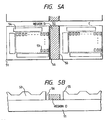
- Figs. 5A and 5B are plan views of a wafer when the present invention is applied to an area sensor;
- Fig. 6 is a plan view showing a wafer to explain Example 1;
- Fig. 7 is a plan view showing a wafer to explain Example 2;
- Fig. 8 is a mounting layout view showing a multi-chip type color image sensor to explain Example 3;
- Fig. 9 is a sectional view of a conventional color image sensor;
- Figs. 10A to 10C are sectional views showing a state wherein the conventional color image sensor is coated with a color filter without planarizing scribe grooves; and
- Figs. 11A to 11F are sectional views showing the flow of a color filter process of the conventional color image sensor.
- The preferred embodiments of the present invention will be described in detail below with reference to the accompanying drawings. Fig. 1A is a plan view of a solid-state image pickup device, Fig. 1B is a sectional view of the device taken along a
line 1B - 1B in Fig. 1A, and Fig. 1C is a sectional view of the device taken along aline 1C - 1C in Fig. 1A. In Fig. 1B, a photoelectric conversion portion (a region A), a peripheral portion (a region B) including switches, wiring layers, and the like, and a scribe region (a region C) are formed on asemiconductor substrate 11. In Fig. 1A, aregion 12 corresponds to the scribe region C as a boundary in the up-and-down direction, and of this region, only the scribe region D as a boundary in the right-and-left direction has the same film structure as that of the photoelectric conversion portion A. Fig. 1C is a sectional view taken along aline 1C - 1C in Fig. 1A. The photoelectric conversion portion (region A) in Fig. 1B comprises a photodiode, and a bipolar type photosensor, or a MOS type photosensor such as a CMD, and the present invention is not limited to a specific photoelectric conversion element. Independently of the photosensor to be adopted, a sensor portion is formed on thesemiconductor substrate 11, and a transparent insulating layer is formed thereon. In Figs. 1A to 1C, a two-layered metal wiring process has been exemplified. However, the present invention is not limited to this process. - In Figs. 1A to 1C, an insulating
layer 13 consists of, e.g., SiO2, and normally has a thickness of 100 nm or less, e.g., about 300 Å. Apolysilicon layer 14 forms electrodes and wiring lines and normally has a thickness of 500 nm or less. An insulatinglayer 15 for isolating between ametal wiring layer 16 and thepolysilicon layer 14 consists of NSG, PSG, SiN, or the like, and normally has a thickness of 1,000 nm or less. An insulatinglayer 17 isolates between ametal wiring layer 18 and themetal wiring layer 16, and has the same material and thickness as those of the insulatinglayer 15. A passivation layer (protection film) 19 has the same material and thickness as those of the insulatinglayer 15. ALOCOS oxide film 10 consists of local silicon oxide, and normally has a thickness of 1 µm or less. Assuming that theLOCOS oxide film 10, the insulatinglayer 13, the insulatinglayer 15, the insulatinglayer 17, and thepassivation layer 19 respectively have thicknesses of 700 nm, 25 nm, 700 nm, 700 nm, and 900 nm, and thepolysilicon layer 14, themetal wiring layer 16, and themetal wiring layer 18 respectively have thicknesses of 400 nm, 800 nm, and 1,200 nm, the heights of the regions A, B, D, and C with reference to the surface of thesemiconductor substrate 11 are respectively about 2.3 µm, 5 µm, 2.3 µm, and 0.1 µm. - Figs. 2A and 2B show a state wherein the above-mentioned semiconductor substrate is coated with a given color filter without any planarizing process. Figs. 2A and 2B correspond to the section portion of the surface portion shown in Fig. 1B. Fig. 2B shows the region A corresponding to a photoelectric conversion portion (23) near the scribe region D (22) at the chip edge, and Fig. 2A shows the region A corresponding to a photoelectric conversion portion (21) at the center of the chip. Since the scribe region D (22) has substantially the same height as that of the region A corresponding to the photoelectric conversion portion (23), coating nonuniformity can be greatly eliminated as compared to a conventional structure.
- Figs. 3A and 3B show a state wherein coating of the substrate with a
color filter 34 is performed after only the planarizing process of the photoelectric conversion portion is performed. Fig. 3A shows a structure in which ared filter 34 is formed by coating on the centralphotoelectric conversion portion 21 corresponding to an intermediate region betweenadjacent scribe regions 22, and Fig. 3B shows a structure in which ared filter 34 is formed by coating on thephotoelectric conversion portion 23 near thescribe region 22. In this case as well, since the scribe region D has substantially the same structure and height as those of the photoelectric conversion portion (23), the color filters (34) formed by coating on the photoelectric conversion portion (23) at the chip edge and the photoelectric conversion portion (21) at the center of the chip have substantially the same thicknesses. - When the substrate is directly coated with the color filter without performing the planarizing process of the scribe region and the planarizing process of the photoelectric conversion portion in the conventional process, a variation between bits, on the central portion of the chip and on a portion near the scribe region, in the photoelectric conversion portion can be eliminated although the sensitivity slightly deteriorates due to a slightly distorted color filter shape. Therefore, since the planarizing processes can be omitted, an inexpensive color image sensor can be provided. Even when the planarizing process is performed to improve the optical sensitivity of the photoelectric conversion elements before coating with the filters, the planarizing process of the scribe region can be omitted, and an inexpensive color image sensor, which is free from a variation between bits, and has performance equivalent to that obtained via the conventional planarizing processes, can be obtained.
- An important point of the present invention is the size of the region D shown in Fig. 1A. The region D will be described below. In order to uniformly coat the color filters, the scribe regions C and D preferably have the same film structure as that of the photoelectric conversion portion A. However, in the separation/mounting process, since the insulating
layers - Fig. 4 is a plan view of a semiconductor substrate on which a line sensor comprising solid-state image pickup devices is formed. In Fig. 4, the line sensor includes
sensor chips 20 using solid-state image pickup chips, ascribe region 12, photoelectric conversion portions A, peripheral circuit portions B, a scribe region C with a step in thescribe region 12, from which insulating layers are removed each time the insulating layer is formed like in the conventional method, scribe regions D in thescribe region 12, which are constituted by layers having the same thicknesses as those of the photoelectric conversion portions A, and driving circuit portions E. - A variation in optical sensitivity of the photoelectric conversion portions A poses a problem in the horizontal direction, i.e., a direction parallel to a
side 46, and a variation in a region between the central portion of the photoelectric conversion portion A and a portion near aside 45 on onechip 20 poses a problem. When the scribe region D is assured to contact theentire side 45, the grooves exist only in the vertical direction. These grooves are periodic and provided equivalently to each pixel, so that very little difference in shape of a filter between pixels is resulted in and, therefore, a sensitivity variation can be greatly eliminated. Since the line sensor satisfies:
the scribe region D is sufficiently small, and the above-mentioned problem associated with the dicing cutter in the mounting process is negligible. However, in order to improve the yield in the mounting process, distances a and b in Fig. 4 other than the size, in the horizontal direction, of the photoelectric conversion portion A must be reduced. However, these widths correspond to those of the driving circuit portion E and the peripheral circuit portion B with large steps on thesensor chip 20, and only the horizontal direction of the photoelectric conversion portion A influences a variation of the photoelectric conversion portion. For this reason, the limit values of the distances a and b are determined by the precision of sensitivity variation and the viscosity of color filters. Since the color filters are required only on the photoelectric conversion portion, but are not required on the portions a and b in the scribe region, the distances a and b can be smaller as the color filters have higher viscosity. - Figs. 5A and 5B are respectively a plan view and a sectional view of a semiconductor substrate on which an area sensor comprising solid-state image pickup devices is formed. Referring to Figs. 5A and 5B, the area sensor includes
sensor chips 51 as solid-state image pickup chips, a scribe region 52,photoelectric conversion portions 53,peripheral circuit portions 54 including driving circuits, a region C with a step in the scribe region 52, and a region D in the scribe region 52, which is constituted by the same layers as those of thephotoelectric conversion portions 53. In the case of the area sensor, a sensitivity variation poses a problem not only in the horizontal direction but also in the vertical direction. Therefore, theperipheral circuit portions 54 and the like are preferably arranged along at least two opposing sides of the region of thephotoelectric conversion portion 53 so as to assure a certain distance between the photoelectric conversion portion and the scribe region in one direction, thereby eliminating sensitivity variation factors. More specifically, in one direction, the photoelectric conversion region is preferably arranged at the center of the chip. - In an example to be described below, the peripheral circuit portions are arranged inside the three sides of the sensor chip, and the photoelectric conversion region is arranged near the center of the chip in the vertical direction in Figs. 5A and 5B. A scribe region in question is the scribe region D contacting a
side 55. In this case, when the region D is assured to contact theentire side 55 like in the line sensor, not only the blade of the dicing cutter but also a decrease in yield of the chips due to cracks formed in insulating layers pose a serious problem. Thus, as shown in Fig. 5B,gaps 56 are formed so that the region D is arranged in an island pattern, thereby suppressing cracks from reaching the interior of the chip. Strictly speaking, coating nonuniformity occurs due to the influence of thegaps 56. However, when thegaps 56 are set to have a minimum rule, a sensitivity variation between bits of thephotoelectric conversion portion 53 after coating with filters can be suppressed. - Since solid-state image pickup devices were formed in practice using the technical concept of the present invention, and their effect were confirmed, these devices will be described below as examples.
- This example will be explained below with reference to Fig. 6. In this example, a CCD color sensor consisting of two polysilicon layers, two aluminum wiring layers, and a light-shielding aluminum layer was manufactured. In Fig. 6, the sensor includes color line sensor chips 61, a scribe region C (62), and
photodiode arrays 63 of photoelectric conversion elements. Of the scribe region C, a silicon surface was exposed from the region C, while a region D was formed to have the same film structure as that of the photodiodes of thephotoelectric conversion portion 63 in such a manner that insulating layers were formed in the same insulating layer forming process, and the insulating layers were removed by patterning from only the scribe region C parallel to the longitudinal direction of thephotoelectric conversion portion 63. - In this example, in the
photodiode portion 63 as the photoelectric conversion portion and the scribe region D, a gate oxide film consisting of silicon thermal oxide, a first insulating layer for isolating between first and second polysilicon layers, and a first aluminum wiring layer, a second insulating layer for isolating between the first aluminum wiring layer and a second aluminum wiring layer, a third insulating layer for isolating between the second aluminum wiring layer and a light-shielding aluminum layer, and a passivation layer were deposited in turn on the surface of asemiconductor substrate 11. - A line sensor using a CCD for charge transfer was manufactured in such a manner that only a planarizing process for filling grooves of the
photoelectric conversion portions 63 was performed on thesemiconductor substrate 11, one color filter was formed by coating and patterning to remove a portion except for necessary color filter portions so as to sequentially form red, blue, and green filters. - In this formation process, a satisfactory CCD line sensor free from a sensitivity variation between bits was manufactured without performing any planarizing process of scribe grooves. Since the step between the scribe region D and the region C was about 3 µm, if no planarizing process of scribe grooves was performed in the conventional method, the color filter flowed into the grooves of the scribe region, and the color filters have different shapes on a portion in the vicinity of the scribe region and at the central portion of the chip, thus causing a sensitivity variation between bits. As compared to the conventional method of avoiding coating nonuniformity of the color filters due to the presence of scribe grooves by separating the photoelectric conversion portion from the chip edge after only the planarizing process of the grooves of the photoelectric conversion portions was performed, the number of chips which could be cut per wafer could be improved by 5% although the processes remained the same.
- Example 2 will be explained below with reference to Fig. 7. In this example, a base accumulation bipolar transistor type color line sensor consisting of one polysilicon layer, and two aluminum wiring layers was manufactured. In Fig. 7, the sensor includes color
line sensor chips 71, ascribe region 72, andphotoelectric conversion portions 73. Of thescribe region 72, a silicon surface was exposed from a region C, while a region D was manufactured to have the same film structure as that of the photoelectric conversion portion. In this example, in thephotoelectric conversion portion 73 and the region D, a gate oxide film consisting of silicon thermal oxide, a first insulating layer for isolating between first and second polysilicon layers, and a first aluminum wiring layer, a second insulating layer for isolating between the first aluminum wiring layer and a second aluminum wiring layer, and a passivation layer were deposited in turn on the surface of a semiconductor substrate. - A base accumulation bipolar transistor type color line sensor was manufactured in such a manner that only a planarizing process for filling grooves of the
photoelectric conversion portions 73 was performed with respect to the semiconductor substrate, and a color filter was formed by coating and patterning to sequentially form red, blue, and green filters. In this case, the step between the regions D and C of thescribe region 72 was about 2 µm or more. In this example, the same effect as in Example 1 was obtained. - Following the same processes as in the base accumulation bipolar transistor type color line sensor manufactured in Example 2, color line sensor chips having 158 bits x 3 colors per chip were formed. The distances L2, L3, and Lp described above was set to be 15 µm, 8 µm, and 20 µm, respectively, and 10 color sensor chips were aligned in line to manufacture an A4-size paper equal-magnification system multi-chip type color line sensor that could directly read an original (see Fig. 8). Since the multi-chip structure was adopted, the minimum distance between the photoelectric conversion portion and the scribe region was 8 µm. However, a low-cost multi-chip type color image sensor free from a sensitivity variation between bits due to the color filter shape difference could be manufactured without performing any scribe groove planarizing process.
- In this example, a CCD color area sensor consisting of two polysilicon layers, two aluminum wiring layers, and a light-shielding aluminum layer was manufactured. The
photoelectric conversion portion 53 and theperipheral circuit portions 54 were arranged, as shown in Figs. 5A and 5B. On the other hand, the region D of the scribe region 52 was formed in an island pattern. In Figs. 5A and 5B, thegap 56 between the,chip 51 and the scribe region D was set to be 2 µm. The film structure of the photodiode portion as thephotoelectric conversion portion 53 and the region D was the same as that in Example 1. As for coating nonuniformity of color filters, the same effect as in Example 1 was obtained. Since the area sensor was manufactured, the area of the region D was larger than that in the line sensor. For this reason, if the region D was formed adjacent to the chip as in Examples 1 to 3, the yield lowered due to cracks formed in insulating layers upon dicing. However, since the 2-µmwide gap 56 was assured like in this example, a decrease in yield due to cracks could be prevented. Such an arrangement can be applied to the line sensor. - For example, a plurality of solid-state image pickup chips cut along the regions D in each of the above-mentioned examples are aligned in a line to constitute a line sensor for directly reading a real-size original image. In this case, the pitch between the photoelectric conversion portion at the chip edge portion and that on an adjacent chip is set to be equal to the pitch between other photoelectric conversion portions as much as possible. However, the regions D cannot be entirely removed, and they inevitably remain to some extent so as not to cause cracking of the photoelectric conversion portions upon cutting. Therefore, the regions D at the edge portions of the chip are not perfectly removed by practicing the present invention. The distance L2 between chips shown in Fig. loc can be set to be about 20 µm in correspondence with the NTSC system.
- As described above, according to the present invention, when a portion, where adjacent sensor chips are connected to each other in terms of a structure, of the scribe region is designed to have the same film structure as that on the photoelectric conversion portion, the planarizing process of scribe grooves can be omitted, and filter portions near the scribe region and separated from the scribe region can have the same film thickness. Even when the photoelectric conversion portion is arranged near the scribe region, a sensitivity variation between bits caused by the non-uniform thicknesses of color filters can be suppressed. As a result, a low-cost color sensor can be provided.
characterised by;
forming on said laterally extending portions of said scribe region to the exclusion of said longitudinally extending portions; thereof, before the colour filter layer is applied to the photoelectric conversion portion, a covering that is constituted by a respective portion of all said plurality of intermediate covering layers;
whereby the surface of said covering is substantially level with the interface of said colour filter layer with the immediately adjacent one of said intermediate covering layers, whereas the surface at said longitudinally extending portion of said scribe region, is at a lower level.
Claims (10)
- A semiconductor wafer comprising a plurality of solid-state pick-up chips (20;51;61;71) each of which includes a respective photoelectric conversion portion (A;21) comprising a plurality of longitudinally arranged photoelectric conversion elements (53;63;73), a respective peripheral circuit portion (B,E;54;64;74), a colour filter layer (24;34:RGB) disposed over said respective photoelectric conversion portion, -and a plurality of intermediate covering layers (13,15,17,19;-) between said colour filter layer and said respective photoelectric conversion portion, and also a scribe region (C,D: 12,22; 52,D; 62,D; 72,D) for separating said solid-state pick-up chips, having longitudinally extending portions (C:12;52;62;72) and, transverse to these, laterally extending portions (D:22) located between longitudinally arranged neighbouring ones of said solid-state pick-up chips, bounded by said longitudinally extending portions of said scribe region;
characterised by:said laterally extending portions (D;22) of said scribe region (C,D:12,22;52,D;62,D;72,D) to the exclusion of said longitudinally extending portions (C;12;52;62;72) thereof, having a covering (13-15,17,19;-) that is constituted by a respective portion of all said plurality of intermediate covering layers (13,15,17,19;-),whereby the surface of said covering (13,15,17,19) is substantially level with the interface of said colour filter layer (24;34:RGB) with the immediately adjacent one (19;-) of said intermediate covering layers (13,15,17,19;-), whereas the surface at said longitudinally extending portion (C;12;52;62;72) of said scribe region, is at a lower level. - A semiconductor wafer according to claim 1, wherein when each of said solid-state pick-up chips (51) constitutes an area sensor wherein said photoelectric conversion elements (53) are arranged laterally as well as longitudinally, said peripheral circuit portion (54) is located adjacent the photoelectric conversion portion along two longitudinal and one lateral sides thereof, and along the second lateral side thereof, the photoelectric conversion portion is separated from the scribe region (D) by a groove (56).
- A semiconductor wafer according to claim 1, wherein said peripheral circuit portion (64) is arranged adjacent two mutually orthogonal sides of the photoelectric conversion portion.
- A solid-state image pick-up device of a chip arrangement type, comprising an arrangement of a plurality of solid-state pick-up chips, each of which has been separated from a semiconductor wafer according to claim 1, 2 or 3.
- A solid-state pick-up chip (20;51;61;71) including a photoelectric conversion portion (A;21) comprising a plurality of longitudinally arranged photoelectric conversion elements (53;63;73), a peripheral circuit portion (B,E;54;64;74), a colour filter layer (24;34:RGB) disposed over said photoelectric conversion portion, and a plurality of intermediate covering layers (15,15,17, 19;-) between said colour filter layer and said photoelectric conversion portion, and also scribed edge portions (C,D;12,22;52,D;62,D;72,D) having longitudinally extending edge portions (C;12;52;62;72) along the edges of the pick-up chip parallel to the longitudinally arranged photoelectric conversion elements (53;63;73), and transverse to these, laterally extending edge portions (D;22) along the remaining edges of the pick-up chip;
characterised by:said laterally extending scribed edge portions (D;22) of said scribed edge portions (C,D;12,22;52,D;62,D;72,D) to the exclusion of said longitudinally extending scribed edge portions (C;12;52;62;72) thereof, having a covering (13,15,17,19;-) that is constituted by a respective portion of all said plurality of intermediate covering layers (13,15,17,19:-),whereby the surface of said covering (13,15,17,19) is substantially level with the interface of said colour filter layer (24;34:RGB) with the immediately adjacent one (19;-) of said intermediate covering layers (13,15,17,19;-), wherein the surface at said longitudinally extending scribed edge portions (C;12;52;62;72) is at a lower level. - A chip according to claim 5, wherein when the chip (51) constitutes an area sensor wherein said photoelectric conversion elements (53) are arranged laterally as well as longitudinally, said peripheral circuit portion (54) is located adjacent the photoelectric conversion portion along two longitudinal and one lateral sides thereof, and along the second lateral side thereof, the photoelectric conversion portion is separated from the scribed edge portion (D) by a groove (56).
- A chip according to claim 5, wherein said peripheral circuit portion (64) is arranged adjacent two mutually orthogonal sides of the photoelectric conversion portion.
- A solid-state image pick-up device, comprising an array of mounted solid-state pick-up chips each being a chip according to any of claims 5, 6 or 7.
- A method of forming a solid-state image pickup device comprising steps of:forming on a semiconductor wafer a plurality of solid-state pick-up chips (20;51;61;71) each of which includes a respective photoelectric conversion portion (A; 21) comprising a plurality of photoelectric conversion elements (53;63;73)' and a respective peripheral circuit region (B,E,54;64,74), wherein the photoelectric conversion portion is formed by providing a number of covering layers (13, 15, 17, 19, 24; 34: RGB) disposed over said respective photoelectric conversion portion, comprising intermediate covering layers (13,15,17,19;-) and a colour filter layer (24;34:RGB);providing between each of the solid-state pick-up chips (20;51;61;71) a scribe region (C,D;12,22;52,D;62,D;72,D), the scribe region having longitudinally extending portions (C;12;52;62;72) and, transverse to these, laterally extending portions (D;22) located between longitudinally arranged neighbouring ones of said solid-state pick-up chips, bounded by said longitudinally extending portions of said scribe region;separating the solid-state pick-up chips by scribing along both portions of the scribing region to produce a plurality of separate solid-state pick-up chips; andproducing the solid-state image pick-up device by mounting and wiring a plurality of the separate solid-state pickup-chips in an array formation;
characterised by;
forming on said laterally extending portions (D;22) of said scribe region (C,D;12,22;52D;62,D;72,D) to the exclusion of said longitudinally extending portions (C; 12;52;62;72) thereof, before the colour filter layer is applied to the photoelectric conversion portion, a covering (13,15,17,19:-) that is constituted by a respective portion of all said plurality of intermediate covering layers (13,15,17,19;-);
whereby the surface of said covering (13,15,17,19) is substantially level with the interface of said colour filter layer (24;34;REB) with the immediately adjacent one (19;-) of said intermediate covering layers (13,15,17,19;-), whereas the surface at said longitudinally extending portion (C;12;52;62;72) of said scribe region, is at a lower level. - A method according to claim 9, wherein said step:of providing the colour filter layer (24;34;RGB) comprises repeatedly coating and patterning the photoelectric conversion portion.
Applications Claiming Priority (2)
| Application Number | Priority Date | Filing Date | Title |
|---|---|---|---|
| JP643/95 | 1995-01-06 | ||
| JP64395A JPH08186241A (en) | 1995-01-06 | 1995-01-06 | Imaging element and solid-state imaging device |
Publications (3)
| Publication Number | Publication Date |
|---|---|
| EP0721220A2 EP0721220A2 (en) | 1996-07-10 |
| EP0721220A3 EP0721220A3 (en) | 1997-07-16 |
| EP0721220B1 true EP0721220B1 (en) | 2006-02-22 |
Family
ID=11479392
Family Applications (1)
| Application Number | Title | Priority Date | Filing Date |
|---|---|---|---|
| EP96300097A Expired - Lifetime EP0721220B1 (en) | 1995-01-06 | 1996-01-04 | Image pickup element and image pickup device |
Country Status (4)
| Country | Link |
|---|---|
| US (1) | US5698892A (en) |
| EP (1) | EP0721220B1 (en) |
| JP (1) | JPH08186241A (en) |
| DE (1) | DE69635837D1 (en) |
Families Citing this family (44)
| Publication number | Priority date | Publication date | Assignee | Title |
|---|---|---|---|---|
| DE19607047C2 (en) * | 1996-02-24 | 1999-03-25 | Gen Semiconductor Ireland Macr | Method for manufacturing semiconductor elements with active structures |
| TW303982U (en) * | 1996-06-28 | 1997-04-21 | Winbond Electronics Corp | Structure of chip guard ring using contact via |
| TW311242B (en) * | 1996-12-12 | 1997-07-21 | Winbond Electronics Corp | Die seal structure with trench and manufacturing method thereof |
| US5789302A (en) * | 1997-03-24 | 1998-08-04 | Siemens Aktiengesellschaft | Crack stops |
| JP4271268B2 (en) | 1997-09-20 | 2009-06-03 | 株式会社半導体エネルギー研究所 | Image sensor and image sensor integrated active matrix display device |
| TW421962B (en) | 1997-09-29 | 2001-02-11 | Canon Kk | Image sensing device using mos type image sensing elements |
| TW428243B (en) * | 1999-01-22 | 2001-04-01 | United Microelectronics Corp | Method for enhancing the planarization of the die region and scribe line by using dummy pattern |
| US7324144B1 (en) * | 1999-10-05 | 2008-01-29 | Canon Kabushiki Kaisha | Solid image pickup device, image pickup system and method of driving solid image pickup device |
| JP3467013B2 (en) * | 1999-12-06 | 2003-11-17 | キヤノン株式会社 | Solid-state imaging device |
| US6998595B2 (en) * | 2001-03-08 | 2006-02-14 | Xerox Corporation | Color filter configuration for a silicon wafer to be diced into photosensitive chips |
| FR2829875B1 (en) * | 2001-09-14 | 2004-01-02 | Atmel Grenoble Sa | IMAGE SENSOR WITH PLANARIZING LAYERS AND MANUFACTURING PROCESS |
| EP1341377B1 (en) | 2002-02-27 | 2018-04-11 | Canon Kabushiki Kaisha | Signal processing device for image pickup apparatus |
| US7507598B2 (en) * | 2003-06-06 | 2009-03-24 | Taiwan Semiconductor Manufacturing Co., Ltd. | Image sensor fabrication method and structure |
| JP4756839B2 (en) | 2004-09-01 | 2011-08-24 | キヤノン株式会社 | Solid-state imaging device and camera |
| JP4459064B2 (en) * | 2005-01-14 | 2010-04-28 | キヤノン株式会社 | Solid-state imaging device, control method thereof, and camera |
| JP4416668B2 (en) * | 2005-01-14 | 2010-02-17 | キヤノン株式会社 | Solid-state imaging device, control method thereof, and camera |
| JP2006197392A (en) * | 2005-01-14 | 2006-07-27 | Canon Inc | Solid-state imaging device, camera, and driving method of solid-state imaging device |
| JP4459098B2 (en) * | 2005-03-18 | 2010-04-28 | キヤノン株式会社 | Solid-state imaging device and camera |
| JP4459099B2 (en) | 2005-03-18 | 2010-04-28 | キヤノン株式会社 | Solid-state imaging device and camera |
| JP4677258B2 (en) * | 2005-03-18 | 2011-04-27 | キヤノン株式会社 | Solid-state imaging device and camera |
| JP4794877B2 (en) * | 2005-03-18 | 2011-10-19 | キヤノン株式会社 | Solid-state imaging device and camera |
| JP4849509B2 (en) * | 2005-06-21 | 2012-01-11 | シャープ株式会社 | SEMICONDUCTOR DEVICE, ITS MANUFACTURING METHOD, AND ELECTRONIC INFORMATION DEVICE |
| JP2007201009A (en) * | 2006-01-24 | 2007-08-09 | Fujifilm Corp | Solid-state image sensor |
| KR101255334B1 (en) * | 2006-05-08 | 2013-04-16 | 페어차일드코리아반도체 주식회사 | Power module for low thermal resistance and method of fabricating of the same power module |
| JP4185949B2 (en) | 2006-08-08 | 2008-11-26 | キヤノン株式会社 | Photoelectric conversion device and imaging device |
| JP4928199B2 (en) * | 2006-09-07 | 2012-05-09 | キヤノン株式会社 | Signal detection device, signal readout method of signal detection device, and imaging system using signal detection device |
| EP2037667B1 (en) * | 2007-09-14 | 2017-08-23 | Canon Kabushiki Kaisha | Image sensing apparatus and imaging system |
| KR100856950B1 (en) * | 2007-12-22 | 2008-09-04 | 주식회사 동부하이텍 | Image sensor and its manufacturing method |
| JP5328207B2 (en) * | 2008-04-01 | 2013-10-30 | キヤノン株式会社 | Solid-state imaging device |
| JP5025596B2 (en) * | 2008-08-20 | 2012-09-12 | 株式会社半導体エネルギー研究所 | Image sensor |
| US8560957B2 (en) * | 2008-10-13 | 2013-10-15 | Autodesk, Inc. | Data-driven interface for managing materials |
| JP4873001B2 (en) | 2008-12-10 | 2012-02-08 | ソニー株式会社 | Solid-state imaging device and manufacturing method thereof, electronic apparatus, and semiconductor device |
| US8624971B2 (en) * | 2009-01-23 | 2014-01-07 | Kla-Tencor Corporation | TDI sensor modules with localized driving and signal processing circuitry for high speed inspection |
| JP5478905B2 (en) * | 2009-01-30 | 2014-04-23 | キヤノン株式会社 | Solid-state imaging device |
| JP5679653B2 (en) | 2009-12-09 | 2015-03-04 | キヤノン株式会社 | Photoelectric conversion device and imaging system using the same |
| JP5780711B2 (en) | 2010-04-06 | 2015-09-16 | キヤノン株式会社 | Solid-state imaging device |
| JP5510053B2 (en) * | 2010-05-14 | 2014-06-04 | 凸版印刷株式会社 | Manufacturing method of color filter for linear sensor |
| JP6403369B2 (en) * | 2013-09-18 | 2018-10-10 | ローム株式会社 | Photodetector and sensor package |
| JP6541347B2 (en) | 2014-03-27 | 2019-07-10 | キヤノン株式会社 | Solid-state imaging device and imaging system |
| JP6548391B2 (en) | 2014-03-31 | 2019-07-24 | キヤノン株式会社 | Photoelectric conversion device and imaging system |
| JP6492991B2 (en) * | 2015-06-08 | 2019-04-03 | 株式会社リコー | Solid-state imaging device |
| US9900539B2 (en) | 2015-09-10 | 2018-02-20 | Canon Kabushiki Kaisha | Solid-state image pickup element, and image pickup system |
| JP6740067B2 (en) | 2016-09-16 | 2020-08-12 | キヤノン株式会社 | Solid-state imaging device and driving method thereof |
| JP6750876B2 (en) | 2016-10-07 | 2020-09-02 | キヤノン株式会社 | Solid-state imaging device and driving method thereof |
Family Cites Families (7)
| Publication number | Priority date | Publication date | Assignee | Title |
|---|---|---|---|---|
| JPS6321604A (en) * | 1986-07-16 | 1988-01-29 | Matsushita Electronics Corp | Manufacture of color filter |
| US5135891A (en) * | 1988-01-19 | 1992-08-04 | Mitsubishi Denki Kabushiki Kaisha | Method for forming film of uniform thickness on semiconductor substrate having concave portion |
| JPH02264468A (en) * | 1989-04-05 | 1990-10-29 | Mitsubishi Electric Corp | Manufacture of solid-state image sensor |
| US5136354A (en) * | 1989-04-13 | 1992-08-04 | Seiko Epson Corporation | Semiconductor device wafer with interlayer insulating film covering the scribe lines |
| JPH0314268A (en) * | 1989-06-13 | 1991-01-22 | Mitsubishi Electric Corp | Manufacture of color image sensor |
| US5191406A (en) * | 1990-04-20 | 1993-03-02 | Nikon Corporation | Method and apparatus for rapid scanning of color images |
| JP2853785B2 (en) * | 1992-01-30 | 1999-02-03 | 松下電子工業株式会社 | Solid-state imaging device and manufacturing method thereof |
-
1995
- 1995-01-06 JP JP64395A patent/JPH08186241A/en active Pending
-
1996
- 1996-01-02 US US08/581,904 patent/US5698892A/en not_active Expired - Fee Related
- 1996-01-04 EP EP96300097A patent/EP0721220B1/en not_active Expired - Lifetime
- 1996-01-04 DE DE69635837T patent/DE69635837D1/en not_active Expired - Lifetime
Also Published As
| Publication number | Publication date |
|---|---|
| JPH08186241A (en) | 1996-07-16 |
| US5698892A (en) | 1997-12-16 |
| EP0721220A2 (en) | 1996-07-10 |
| DE69635837D1 (en) | 2006-04-27 |
| EP0721220A3 (en) | 1997-07-16 |
Similar Documents
| Publication | Publication Date | Title |
|---|---|---|
| US5698892A (en) | Image pickup element and image pickup device having scribe lines composed of two portions with different layer structure | |
| KR100477789B1 (en) | Method for fabricating image sensor | |
| US7858433B2 (en) | Photoelectric converting film stack type solid-state image pickup device, and method of producing the same | |
| EP0945743B1 (en) | Solid-state image sensing device and method for manufacturing the same | |
| US6348361B1 (en) | CMOS image sensor having enhanced photosensitivity and method for fabricating the same | |
| US20110165723A1 (en) | Solid-state imaging device and method of manufacturing solid-state imaging device | |
| KR19990073943A (en) | Solid color image device and its manufacturing method | |
| KR20000041461A (en) | Fabrication method of improved image sensor | |
| US20230082070A1 (en) | Image sensor and method of manufacturing the same | |
| EP0557135B1 (en) | Image sensor color filters | |
| KR840002299B1 (en) | Manufacturing method of color solid state image pickup device | |
| CN100413079C (en) | Method for making image sensor with recessed planarization layer | |
| KR20010061308A (en) | Method for fabricating thin film image sensor | |
| US20250204067A1 (en) | Image sensor including separation structure | |
| US5696626A (en) | Photosensitive silicon chip having a ridge near an end photosite | |
| KR100329782B1 (en) | Method for fabricating image sensor with improved photo sensitivity | |
| US7608871B2 (en) | Solid image pick-up element with a single layer electrode structure and method of producing the same | |
| JP4905760B2 (en) | Color filter manufacturing method, color filter, solid-state image sensor manufacturing method, and solid-state image sensor using the same | |
| US20060270120A1 (en) | IT-CCD and manufacturing method thereof | |
| KR20010061343A (en) | Method for fabricating image sensor | |
| KR20010061056A (en) | Method for fabricating image sensor with improved light sensitivity | |
| KR100489351B1 (en) | Manufacturing method of image sensor with protective film to which planarization process is applied | |
| KR20030039713A (en) | Image sensor and method of fabricating the same | |
| US20020192970A1 (en) | Method for manufacturing charge-coupled image sensors | |
| JP2001196571A (en) | Solid-state imaging device |
Legal Events
| Date | Code | Title | Description |
|---|---|---|---|
| PUAI | Public reference made under article 153(3) epc to a published international application that has entered the european phase |
Free format text: ORIGINAL CODE: 0009012 |
|
| AK | Designated contracting states |
Kind code of ref document: A2 Designated state(s): DE FR GB IT NL |
|
| PUAL | Search report despatched |
Free format text: ORIGINAL CODE: 0009013 |
|
| AK | Designated contracting states |
Kind code of ref document: A3 Designated state(s): DE FR GB IT NL |
|
| 17P | Request for examination filed |
Effective date: 19971126 |
|
| 17Q | First examination report despatched |
Effective date: 19991223 |
|
| GRAP | Despatch of communication of intention to grant a patent |
Free format text: ORIGINAL CODE: EPIDOSNIGR1 |
|
| GRAS | Grant fee paid |
Free format text: ORIGINAL CODE: EPIDOSNIGR3 |
|
| GRAA | (expected) grant |
Free format text: ORIGINAL CODE: 0009210 |
|
| AK | Designated contracting states |
Kind code of ref document: B1 Designated state(s): DE FR GB IT NL |
|
| PG25 | Lapsed in a contracting state [announced via postgrant information from national office to epo] |
Ref country code: NL Free format text: LAPSE BECAUSE OF FAILURE TO SUBMIT A TRANSLATION OF THE DESCRIPTION OR TO PAY THE FEE WITHIN THE PRESCRIBED TIME-LIMIT Effective date: 20060222 Ref country code: IT Free format text: LAPSE BECAUSE OF FAILURE TO SUBMIT A TRANSLATION OF THE DESCRIPTION OR TO PAY THE FEE WITHIN THE PRESCRIBED TIME-LIMIT;WARNING: LAPSES OF ITALIAN PATENTS WITH EFFECTIVE DATE BEFORE 2007 MAY HAVE OCCURRED AT ANY TIME BEFORE 2007. THE CORRECT EFFECTIVE DATE MAY BE DIFFERENT FROM THE ONE RECORDED. Effective date: 20060222 |
|
| REG | Reference to a national code |
Ref country code: GB Ref legal event code: FG4D |
|
| REF | Corresponds to: |
Ref document number: 69635837 Country of ref document: DE Date of ref document: 20060427 Kind code of ref document: P |
|
| PG25 | Lapsed in a contracting state [announced via postgrant information from national office to epo] |
Ref country code: DE Free format text: LAPSE BECAUSE OF FAILURE TO SUBMIT A TRANSLATION OF THE DESCRIPTION OR TO PAY THE FEE WITHIN THE PRESCRIBED TIME-LIMIT Effective date: 20060523 |
|
| NLV1 | Nl: lapsed or annulled due to failure to fulfill the requirements of art. 29p and 29m of the patents act | ||
| PLBE | No opposition filed within time limit |
Free format text: ORIGINAL CODE: 0009261 |
|
| STAA | Information on the status of an ep patent application or granted ep patent |
Free format text: STATUS: NO OPPOSITION FILED WITHIN TIME LIMIT |
|
| 26N | No opposition filed |
Effective date: 20061123 |
|
| EN | Fr: translation not filed | ||
| PG25 | Lapsed in a contracting state [announced via postgrant information from national office to epo] |
Ref country code: FR Free format text: LAPSE BECAUSE OF FAILURE TO SUBMIT A TRANSLATION OF THE DESCRIPTION OR TO PAY THE FEE WITHIN THE PRESCRIBED TIME-LIMIT Effective date: 20070309 |
|
| PG25 | Lapsed in a contracting state [announced via postgrant information from national office to epo] |
Ref country code: FR Free format text: LAPSE BECAUSE OF FAILURE TO SUBMIT A TRANSLATION OF THE DESCRIPTION OR TO PAY THE FEE WITHIN THE PRESCRIBED TIME-LIMIT Effective date: 20060222 |
|
| PGFP | Annual fee paid to national office [announced via postgrant information from national office to epo] |
Ref country code: GB Payment date: 20130123 Year of fee payment: 18 |
|
| GBPC | Gb: european patent ceased through non-payment of renewal fee |
Effective date: 20140104 |
|
| PG25 | Lapsed in a contracting state [announced via postgrant information from national office to epo] |
Ref country code: GB Free format text: LAPSE BECAUSE OF NON-PAYMENT OF DUE FEES Effective date: 20140104 |