EP0720219A2 - Conductive runner fabrication for an integrated circuit - Google Patents
Conductive runner fabrication for an integrated circuit Download PDFInfo
- Publication number
- EP0720219A2 EP0720219A2 EP96300023A EP96300023A EP0720219A2 EP 0720219 A2 EP0720219 A2 EP 0720219A2 EP 96300023 A EP96300023 A EP 96300023A EP 96300023 A EP96300023 A EP 96300023A EP 0720219 A2 EP0720219 A2 EP 0720219A2
- Authority
- EP
- European Patent Office
- Prior art keywords
- conductive material
- layer
- runners
- thickness
- blanket
- Prior art date
- Legal status (The legal status is an assumption and is not a legal conclusion. Google has not performed a legal analysis and makes no representation as to the accuracy of the status listed.)
- Withdrawn
Links
Images

Classifications
-
- H—ELECTRICITY
- H01—ELECTRIC ELEMENTS
- H01L—SEMICONDUCTOR DEVICES NOT COVERED BY CLASS H10
- H01L21/00—Processes or apparatus adapted for the manufacture or treatment of semiconductor or solid state devices or of parts thereof
- H01L21/70—Manufacture or treatment of devices consisting of a plurality of solid state components formed in or on a common substrate or of parts thereof; Manufacture of integrated circuit devices or of parts thereof
- H01L21/71—Manufacture of specific parts of devices defined in group H01L21/70
- H01L21/768—Applying interconnections to be used for carrying current between separate components within a device comprising conductors and dielectrics
- H01L21/76838—Applying interconnections to be used for carrying current between separate components within a device comprising conductors and dielectrics characterised by the formation and the after-treatment of the conductors
-
- Y—GENERAL TAGGING OF NEW TECHNOLOGICAL DEVELOPMENTS; GENERAL TAGGING OF CROSS-SECTIONAL TECHNOLOGIES SPANNING OVER SEVERAL SECTIONS OF THE IPC; TECHNICAL SUBJECTS COVERED BY FORMER USPC CROSS-REFERENCE ART COLLECTIONS [XRACs] AND DIGESTS
- Y10—TECHNICAL SUBJECTS COVERED BY FORMER USPC
- Y10S—TECHNICAL SUBJECTS COVERED BY FORMER USPC CROSS-REFERENCE ART COLLECTIONS [XRACs] AND DIGESTS
- Y10S438/00—Semiconductor device manufacturing: process
- Y10S438/927—Electromigration resistant metallization
Definitions
- This invention relates to integrated circuits and methods for their fabrication.
- runners Modern integrated circuits are often fabricated with several layers of conductors, often termed "runners". Usually the runners are formed by depositing a blanket layer of a conductive material such as aluminum. Then a patterned photoresist is formed over the aluminum layer. Using the patterned photoresist as a mask, a plasma etching process is initiated and the aluminum is patterned. The patterned aluminum may then be covered with a dielectric.
- a conductive material such as aluminum.
- the invention includes forming a blanket layer of conductive material overlying a dielectric substrate. Then a blanket etchback procedure is performed to reduce the thickness of the conductive material, thereby producing a second blanket layer of conductive material, Then the second layer of conductive material is patterned to form runners.
- substrate 11 is a dielectric, typically an oxide of silicon, or a dielectric containing substantial amount of an oxide of silicon.
- Reference numeral 13 denotes a runner formed according to conventional techniques.
- Reference numerals 15, 17, and 19 denote some of the grain boundaries in runner 13. It has been observed that runners which have grain boundaries that extend along the principal axis of the runner (such as grain boundaries 19) tend to be susceptible to stress migration failures. Furthermore, runners 13 formed by conventional techniques often have small randomly located grains, such as that denoted by reference numeral 21.
- Applicant has discovered that the resistance of runners to stress migration, and possibly electromigration can be improved if the runner has a more bamboo-like structure. Applicant has discovered that it is desirable to minimize or reduce the number of grain boundaries which have a directional component along the axis of the runner (such as grain boundary 19) and also to reduce the number of small grains such as that indicated by reference numeral 21.
- Runner 13 has a width denoted by w; and height denoted by h.
- reference numeral 31 denotes a substrate which, typically, may be an oxide of silicon or contain a substantial amount of an oxide of silicon. Desirably, substrate 31 is smoothed or planarized.
- Metal layer 33 is formed on top of dielectric 31 desirably, by sputtering, although evaporation or other deposition techniques may also be used.
- the thickness, t, of layer 33 is desirably made to be approximately twice the width of the final desired narrowest runner.
- the grain size of layer 33 is generally proportional to thickness and the density of small grains decreases significantly with increasing deposited - film thickness, t.
- the grain size of the patterned runner is generally proportional to the twice the width of the completed, patterned runner with greatly reduced numbers of small grains, thereby producing a uniform bamboo-like structure.
- aluminum layer 33 has been etched back. Typically, approximately 50% of the thickness t, of aluminum runner 33 has been removed.
- a blanket etch back of aluminum layer 33 may be performed by using a dry etching procedure well known to those skill in the art. Alternatively, the upper half of layer 33 may be anodized, converting it to an oxide. The aluminum oxide is removed in a chemical bath containing phosphoric acid and other etchants such as chromic acid known to those of skill of the art.
- patterned photoresist 37 (Fig. 4) is formed on top of layer 35.
- a dry etching process known to those skill in the art is performed to produce patterned runners 41 and 39.
- runner 41 a portion of patterned runner 41 is illustrated.
- Reference numeral 45 and 47 denote grain boundaries. It will be noted that small grains, such as that designated by reference numeral 21 in Fig. 1 and grains having grain boundaries with components parallel to the long axis of the runner (such as that designated by reference numeral 19 in Fig. 1) generally absent. Thus, runner 41 exhibits greater resistance to stress migration and electromigration.
- the inventive technique may be applied to form aluminum runners. It may also be implored to form aluminum runners from Al-Cu and/or Al-Cu-Si. Furthermore, the inventive technique may also be used to form runners containing principally copper or principally silver.
- the inventive technique may be applied to metal runners formed over conductive underlayers, such as patterned aluminum over TiN and/or Ti and/or a refractory metal silicide. The underlying conductive layer may be patterned together with the aluminum or in a subsequent step.
Abstract
The method of forming runners having superior stress migration characteristics is disclosed. A blanket layer of conductive material 33 is deposited over a dielectric 31. A blanket layer is subjected to a blanket-etch back procedure, thereby reducing its thickness by approximately half. The remaining layer 35 is then patterned to form runners 41, 39. Resulting runners 41, 33 have a superior grain structure and greater resistance to electromigration and stress migration.
Description
- This invention relates to integrated circuits and methods for their fabrication.
- Modern integrated circuits are often fabricated with several layers of conductors, often termed "runners". Usually the runners are formed by depositing a blanket layer of a conductive material such as aluminum. Then a patterned photoresist is formed over the aluminum layer. Using the patterned photoresist as a mask, a plasma etching process is initiated and the aluminum is patterned. The patterned aluminum may then be covered with a dielectric.
- Those concerned with the development of integrated circuits have consistently sought for methods and structures which will improve the electromigration and stress migration properties of aluminum runners.
- The present invention addresses these concerns. Illustratively, the invention includes forming a blanket layer of conductive material overlying a dielectric substrate. Then a blanket etchback procedure is performed to reduce the thickness of the conductive material, thereby producing a second blanket layer of conductive material, Then the second layer of conductive material is patterned to form runners.
-
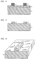
- Fig. 1 is a partially perspective, partially cross sectional view of a typical aluminum runner;
- Figs. 2-5 are cross sectional views useful in understanding an illustrative embodiment of the present invention; and
- Fig. 6 is a partially, perspective partially cross sectional view of an illustrative embodiment of the present invention.
- In Fig. 1, substrate 11 is a dielectric, typically an oxide of silicon, or a dielectric containing substantial amount of an oxide of silicon. Reference numeral 13 denotes a runner formed according to conventional techniques.
Reference numerals reference numeral 21. - Applicant has discovered that the resistance of runners to stress migration, and possibly electromigration can be improved if the runner has a more bamboo-like structure. Applicant has discovered that it is desirable to minimize or reduce the number of grain boundaries which have a directional component along the axis of the runner (such as grain boundary 19) and also to reduce the number of small grains such as that indicated by
reference numeral 21. - Runner 13 has a width denoted by w; and height denoted by h.
- Applicant's process may be understood by reference to Figs.2-5. In Fig. 2
reference numeral 31 denotes a substrate which, typically, may be an oxide of silicon or contain a substantial amount of an oxide of silicon. Desirably,substrate 31 is smoothed or planarized.Metal layer 33 is formed on top of dielectric 31 desirably, by sputtering, although evaporation or other deposition techniques may also be used. The thickness, t, oflayer 33 is desirably made to be approximately twice the width of the final desired narrowest runner. The grain size oflayer 33 is generally proportional to thickness and the density of small grains decreases significantly with increasing deposited - film thickness, t. The grain size of the patterned runner is generally proportional to the twice the width of the completed, patterned runner with greatly reduced numbers of small grains, thereby producing a uniform bamboo-like structure. - Turning to Fig. 3,
aluminum layer 33 has been etched back. Typically, approximately 50% of the thickness t, ofaluminum runner 33 has been removed. A blanket etch back ofaluminum layer 33 may be performed by using a dry etching procedure well known to those skill in the art. Alternatively, the upper half oflayer 33 may be anodized, converting it to an oxide. The aluminum oxide is removed in a chemical bath containing phosphoric acid and other etchants such as chromic acid known to those of skill of the art. After a blanket etch back has been performed to producelayer 35, patterned photoresist 37 (Fig. 4) is formed on top oflayer 35. - Turning to Fig. 5, a dry etching process known to those skill in the art is performed to produce patterned
runners 41 and 39. - Turning to Fig. 6, a portion of patterned runner 41 is illustrated. Reference numeral 45 and 47 denote grain boundaries. It will be noted that small grains, such as that designated by
reference numeral 21 in Fig. 1 and grains having grain boundaries with components parallel to the long axis of the runner (such as that designated by reference numeral 19 in Fig. 1) generally absent. Thus, runner 41 exhibits greater resistance to stress migration and electromigration. - The inventive technique may be applied to form aluminum runners. It may also be implored to form aluminum runners from Al-Cu and/or Al-Cu-Si. Furthermore, the inventive technique may also be used to form runners containing principally copper or principally silver. The inventive technique may be applied to metal runners formed over conductive underlayers, such as patterned aluminum over TiN and/or Ti and/or a refractory metal silicide. The underlying conductive layer may be patterned together with the aluminum or in a subsequent step.
Claims (8)
- A method of forming an integrated circuit comprising:
forming a blanket layer of conductive material (33) overlying a dielectric substrate (31);
performing a blanket etch back procedure to reduce the thickness of said conductive material, thereby producing a second blanket layer of conductive material (35);
patterning said second layer of conductive material to form conductive runners (41, 39). - The method of claim 1 in which one or more material layers are formed between said blanket layer of conductive material (33) and said substrate (31).
- The method of claim 2 in which said material layer is chosen from the group consisting of TiN, Ti, and refractory metal silicides.
- The method of claim 1 in which said conductive material is chosen from the group consisting of Al, Al-Cu, Al-Cu-Si, Ag, and Cu.
- The method of claim 1 in which said thickness is reduced by approximately 50%.
- The method of claim 1 in which said thickness is reduced by anodizing a portion of said conductive material and then wet-etching said anodized portion away.
- The method of claim 1 in which said thickness is reduced by dry etching.
- The method of claim 1 in which said dielectric (31) is smoothed or planarized.
Applications Claiming Priority (2)
| Application Number | Priority Date | Filing Date | Title |
|---|---|---|---|
| US367380 | 1982-04-12 | ||
| US08/367,380 US5599737A (en) | 1994-12-30 | 1994-12-30 | Conductive runner fabrication |
Publications (2)
| Publication Number | Publication Date |
|---|---|
| EP0720219A2 true EP0720219A2 (en) | 1996-07-03 |
| EP0720219A3 EP0720219A3 (en) | 1997-05-07 |
Family
ID=23446935
Family Applications (1)
| Application Number | Title | Priority Date | Filing Date |
|---|---|---|---|
| EP96300023A Withdrawn EP0720219A3 (en) | 1994-12-30 | 1996-01-02 | Conductive runner fabrication for an integrated circuit |
Country Status (3)
| Country | Link |
|---|---|
| US (1) | US5599737A (en) |
| EP (1) | EP0720219A3 (en) |
| JP (1) | JPH08236532A (en) |
Citations (4)
| Publication number | Priority date | Publication date | Assignee | Title |
|---|---|---|---|---|
| US4891112A (en) * | 1985-11-12 | 1990-01-02 | Eastman Kodak Company | Sputtering method for reducing hillocking in aluminum layers formed on substrates |
| US5001541A (en) * | 1989-03-22 | 1991-03-19 | Texas Instruments Incorporated | Advanced electromigration resistant interconnect structure and process |
| US5167760A (en) * | 1989-11-14 | 1992-12-01 | Intel Corporation | Etchback process for tungsten contact/via filling |
| EP0609501A2 (en) * | 1993-01-20 | 1994-08-10 | Kabushiki Kaisha Toshiba | Aluminium based metallization for semiconductor device |
Family Cites Families (6)
| Publication number | Priority date | Publication date | Assignee | Title |
|---|---|---|---|---|
| US5057455A (en) * | 1989-11-30 | 1991-10-15 | At&T Bell Laboratories | Formation of integrated circuit electrodes |
| US5141897A (en) * | 1990-03-23 | 1992-08-25 | At&T Bell Laboratories | Method of making integrated circuit interconnection |
| US5278448A (en) * | 1991-03-19 | 1994-01-11 | Matsushita Electric Industrial Co., Ltd. | Semiconductor device and method of fabricating the same |
| JPH06177127A (en) * | 1991-05-30 | 1994-06-24 | Sony Corp | Formation of wiring |
| JPH04354337A (en) * | 1991-05-31 | 1992-12-08 | Kawasaki Steel Corp | Manufacture of semiconductor device |
| US5202274A (en) * | 1991-06-14 | 1993-04-13 | Samsung Electronics Co., Ltd. | Method of fabricating thin film transistor |
-
1994
- 1994-12-30 US US08/367,380 patent/US5599737A/en not_active Expired - Fee Related
-
1995
- 1995-12-28 JP JP7343003A patent/JPH08236532A/en not_active Withdrawn
-
1996
- 1996-01-02 EP EP96300023A patent/EP0720219A3/en not_active Withdrawn
Patent Citations (4)
| Publication number | Priority date | Publication date | Assignee | Title |
|---|---|---|---|---|
| US4891112A (en) * | 1985-11-12 | 1990-01-02 | Eastman Kodak Company | Sputtering method for reducing hillocking in aluminum layers formed on substrates |
| US5001541A (en) * | 1989-03-22 | 1991-03-19 | Texas Instruments Incorporated | Advanced electromigration resistant interconnect structure and process |
| US5167760A (en) * | 1989-11-14 | 1992-12-01 | Intel Corporation | Etchback process for tungsten contact/via filling |
| EP0609501A2 (en) * | 1993-01-20 | 1994-08-10 | Kabushiki Kaisha Toshiba | Aluminium based metallization for semiconductor device |
Non-Patent Citations (2)
| Title |
|---|
| 26TH ANNUAL PROCEEDINGS RELIABILITY PHYSICS 1988, MONTEREY, APRIL 12 - 14, 1988, no. 1988, 12 April 1988, INSTITUTE OF ELECTRICAL AND ELECTRONICS ENGINEERS, pages 185-191, XP000012743 KWOK T: "EFFECT OF METAL LINE GEOMETRY ON ELECTROMIGRATION LIFETIME IN AL-CU SUBMICRON INTERCONNECTS" * |
| DATABASE INSPEC INSTITUTE OF ELECTRICAL ENGINEERS, STEVENAGE, GB Inspec No. AN5069604, 4 October 1994 RYAN, V; MERCHANT S M: "Enhanced stress-migration reliability for ULSI interconnect: an insight into the perils of screening Al depositions based on grain size" XP002026676 & JOURNAL OF ELECTRONIC MATERIALS, vol. 24, no. 8, August 1995, USA, pages 969-974, XP000618794 RYAN, V; MERCHANT, S M: "Enhanced stress-migration reliability for ULSI interconnect: an insight into the perils of screening Al depositions based on grain size" * |
Also Published As
| Publication number | Publication date |
|---|---|
| US5599737A (en) | 1997-02-04 |
| JPH08236532A (en) | 1996-09-13 |
| EP0720219A3 (en) | 1997-05-07 |
Similar Documents
| Publication | Publication Date | Title |
|---|---|---|
| US5485138A (en) | Thin film resistor and method for manufacturing the same | |
| US5270255A (en) | Metallization process for good metal step coverage while maintaining useful alignment mark | |
| US5369053A (en) | Method for patterning aluminum metallizations | |
| US6469609B2 (en) | Method of fabricating silver inductor | |
| JPS6185879A (en) | Formation of conductive pattern | |
| JPH06140396A (en) | Semiconductor device and manufacture thereof | |
| US6268287B1 (en) | Polymerless metal hard mask etching | |
| US5663102A (en) | Method for forming multi-layered metal wiring semiconductor element using cmp or etch back | |
| JPH0685074A (en) | Manufacture of multilayer interconnection conductor pattern | |
| US5041191A (en) | Diffusion barrier for thin film hybrid circuits | |
| JP2770945B2 (en) | Tungsten coating method | |
| US4717449A (en) | Dielectric barrier material | |
| JPH04369861A (en) | Manufacture of compound semiconductor integrated circuit capacitor | |
| US5599737A (en) | Conductive runner fabrication | |
| US6395629B1 (en) | Interconnect method and structure for semiconductor devices | |
| JP2808616B2 (en) | Method for manufacturing semiconductor device | |
| JP2892337B2 (en) | Method for manufacturing metal wiring of semiconductor element | |
| US4713682A (en) | Dielectric barrier material | |
| US6548413B1 (en) | Method to reduce microloading in metal etching | |
| KR100265839B1 (en) | Metal wiring method for semiconductor device | |
| JPH08186120A (en) | Manufacture of semiconductor device | |
| JPH0341732A (en) | Manufacture of semiconductor device | |
| JPH05226333A (en) | Manufacture of semiconductor device | |
| JP3378693B2 (en) | Method for manufacturing semiconductor device | |
| JPH01102938A (en) | Manufacture of semiconductor integrated circuit |
Legal Events
| Date | Code | Title | Description |
|---|---|---|---|
| PUAI | Public reference made under article 153(3) epc to a published international application that has entered the european phase |
Free format text: ORIGINAL CODE: 0009012 |
|
| AK | Designated contracting states |
Kind code of ref document: A2 Designated state(s): DE FR GB |
|
| PUAL | Search report despatched |
Free format text: ORIGINAL CODE: 0009013 |
|
| AK | Designated contracting states |
Kind code of ref document: A3 Designated state(s): DE FR GB |
|
| 17P | Request for examination filed |
Effective date: 19971023 |
|
| STAA | Information on the status of an ep patent application or granted ep patent |
Free format text: STATUS: THE APPLICATION HAS BEEN WITHDRAWN |
|
| 18W | Application withdrawn |
Withdrawal date: 19980424 |