EP0609501A2 - Aluminium based metallization for semiconductor device - Google Patents
Aluminium based metallization for semiconductor device Download PDFInfo
- Publication number
- EP0609501A2 EP0609501A2 EP93118141A EP93118141A EP0609501A2 EP 0609501 A2 EP0609501 A2 EP 0609501A2 EP 93118141 A EP93118141 A EP 93118141A EP 93118141 A EP93118141 A EP 93118141A EP 0609501 A2 EP0609501 A2 EP 0609501A2
- Authority
- EP
- European Patent Office
- Prior art keywords
- wiring line
- concentration
- size
- alloy
- semiconductor device
- Prior art date
- Legal status (The legal status is an assumption and is not a legal conclusion. Google has not performed a legal analysis and makes no representation as to the accuracy of the status listed.)
- Granted
Links
Images

Classifications
-
- H—ELECTRICITY
- H01—ELECTRIC ELEMENTS
- H01L—SEMICONDUCTOR DEVICES NOT COVERED BY CLASS H10
- H01L21/00—Processes or apparatus adapted for the manufacture or treatment of semiconductor or solid state devices or of parts thereof
- H01L21/02—Manufacture or treatment of semiconductor devices or of parts thereof
- H01L21/04—Manufacture or treatment of semiconductor devices or of parts thereof the devices having at least one potential-jump barrier or surface barrier, e.g. PN junction, depletion layer or carrier concentration layer
- H01L21/18—Manufacture or treatment of semiconductor devices or of parts thereof the devices having at least one potential-jump barrier or surface barrier, e.g. PN junction, depletion layer or carrier concentration layer the devices having semiconductor bodies comprising elements of Group IV of the Periodic System or AIIIBV compounds with or without impurities, e.g. doping materials
- H01L21/30—Treatment of semiconductor bodies using processes or apparatus not provided for in groups H01L21/20 - H01L21/26
- H01L21/31—Treatment of semiconductor bodies using processes or apparatus not provided for in groups H01L21/20 - H01L21/26 to form insulating layers thereon, e.g. for masking or by using photolithographic techniques; After treatment of these layers; Selection of materials for these layers
- H01L21/3205—Deposition of non-insulating-, e.g. conductive- or resistive-, layers on insulating layers; After-treatment of these layers
- H01L21/32051—Deposition of metallic or metal-silicide layers
-
- H—ELECTRICITY
- H01—ELECTRIC ELEMENTS
- H01L—SEMICONDUCTOR DEVICES NOT COVERED BY CLASS H10
- H01L23/00—Details of semiconductor or other solid state devices
- H01L23/52—Arrangements for conducting electric current within the device in operation from one component to another, i.e. interconnections, e.g. wires, lead frames
- H01L23/522—Arrangements for conducting electric current within the device in operation from one component to another, i.e. interconnections, e.g. wires, lead frames including external interconnections consisting of a multilayer structure of conductive and insulating layers inseparably formed on the semiconductor body
- H01L23/532—Arrangements for conducting electric current within the device in operation from one component to another, i.e. interconnections, e.g. wires, lead frames including external interconnections consisting of a multilayer structure of conductive and insulating layers inseparably formed on the semiconductor body characterised by the materials
- H01L23/53204—Conductive materials
- H01L23/53209—Conductive materials based on metals, e.g. alloys, metal silicides
- H01L23/53214—Conductive materials based on metals, e.g. alloys, metal silicides the principal metal being aluminium
-
- H—ELECTRICITY
- H01—ELECTRIC ELEMENTS
- H01L—SEMICONDUCTOR DEVICES NOT COVERED BY CLASS H10
- H01L2924/00—Indexing scheme for arrangements or methods for connecting or disconnecting semiconductor or solid-state bodies as covered by H01L24/00
- H01L2924/0001—Technical content checked by a classifier
- H01L2924/0002—Not covered by any one of groups H01L24/00, H01L24/00 and H01L2224/00
Definitions
- Aluminum is generally used for an electrode wiring line of a semiconductor device in view of a resistance or workability.
- a Cu-added Al alloy is generally used to prevent occurrence of an erroneous wiring line mode such as electro-migration or stress-migration, thereby improving reliability.
- the Al wiring line having a size of several fm larger than the size of Al crystal generally has a point where three grain boundaries between the Al grains overlap, i.e., a triple point of the grain boundaries.
- This phenomenon is called electro-migration. This is caused because the activation energy of the grain boundary of the Al-Cu alloy is about 1.4 eV while the activation energy of the grain boundary is about 0.6 eV, so that the grain boundary serves as a high-speed diffusion path.
- Cu is added to the Al alloy to segregate Cu at the grain boundaries and prevent the Al atoms from diffusing along the grain boundaries.
- the electro-migration life MTF [arb.unit] is prolonged depending on the content of Cu when the Cu concentration is about 8 wt% or less.
- the above-described triple points disappear in the wiring line, leaving bamboo-node-like grain boundaries across the grain size boundaries. More specifically, as the wiring line size becomes larger, the number of triple points of the grain boundaries per unit length is increased, as indicated by a line L2, so that electro-migration tends to occur. On the other hand, as the wiring line size becomes smaller, the number of bamboo-node-like grain boundaries is increased, as indicated by a line L1. The electro-migration life at this time depends on the diffusion speed within the crystal grain, MTF is improved as a whole, and the wiring line life tends to be prolonged.
- the line L1 represents the number of bamboo-node-like grain boundaries per unit length with respect to the line size
- the line L2 represents the number of triple points of the grain boundaries per unit with respect to the line size.
- MTF is improved when the Cu concentration is about 0.1 wt% or less. If the Cu concentration exceeds 0.1 wt%, MTF is degraded.
- the Cu concentration of the current wiring line is determined by the Cu concentration of a spattering target or vapor source, so that all the electrode wiring lines formed in the same process have the same Cu concentration.
- the electrode wiring lines having the same Cu concentration are used although each electrode wiring line ranging from a wiring line having a size in the submicron region to be used as a signal line to a wiring line having a size of 10 fm or more to be used as a power line has an optimal Cu concentration for its size.
- an optimal resistance to electro-migration for wiring lines having different sizes cannot be obtained.
- the present invention has been made to overcome the above drawback, and has as its object to provide a semiconductor device which selects and defines the Cu concentration of the electrode consisting of an Al alloy in accordance with the wiring line size, thereby obtaining an optimal resistance to electro-migration and high reliability.
- a semiconductor device comprising a wiring line formed from an electrode wiring layer using, as an electrode material, an Al alloy containing Cu, wherein a wiring line having a size smaller than a crystal grain size has a Cu concentration of 0.05 to 0.3 wt%, and a wiring line having a size larger than a crystal grain size has a Cu concentration of 0.5 to 10 wt%.
- the semiconductor of the present invention selects and defines the Cu concentration in the Al alloy wiring line in accordance with the wiring line size, thereby obtaining an optimal resistance to electro-migration.
- Figs. 4 to 8 are views showing steps of manufacturing a semiconductor device according to an embodiment of the present invention.
- an Al-Cu alloy 3 serving as an electrode wiring line is formed on the surface of a semiconductor substrate 1 through an insulating film 2.
- a Cu-based material 4 e.g., pure Cu is formed on the Al-Cu alloy 3.
- film formation is performed by the sputtering method, the deposition method can be used in place of the sputtering method.
- the resultant structure constituted by stacking the Al-Cu alloy 3 and the Cu-based material 4 is formed into electrode wiring lines 3-1 and 3-2. More specifically, the wiring line 3-1 having a size smaller than the crystal grain size of the Al-Cu alloy 3 and the wiring line 3-2 having a size larger than the crystal grain size of the Al-Cu alloy 3 are formed to selectively expose the insulating film 2.
- a resist 5 is covered on a part of the exposed portion of the insulating film 2, and the Cu-based material 4.
- the Cu-based material 4 of the wiring line 3-1 having a size smaller than the crystal grain size of the Al-Cu alloy 3 is selectively removed by exposure and development to expose the thin wiring line 3-1.
- the resist 5 is covered on the thick wiring line 3-2.
- the thick wiring line 3-2 shown in Fig. 8 has a higher Cu concentration than that of the thin wiring line 3-1 by a diffusion amount.
- the Cu concentration of the Al-Cu alloy 3 in this embodiment is set in advance to be equal to that of the final wiring line 3-1 having a size smaller than the crystal grain size, the resistance to electro-migration of the wiring line 3-1 having a size smaller than the crystal grain size can be maximized, as shown in Fig. 3.
- Cu must not be segregated in the Al-Cu alloy 3 of the thin wiring line 3-1. Checking the segregated state of Cu, it was confirmed that Cu was not segregated by annealing when the Cu concentration was 0.3 wt% or less.
- the Cu concentration of the Al alloy wiring line having a size smaller than the crystal grain size was in a range of 0.05 to 0.3 wt%. Also in the Al-Cu alloy 3 of this embodiment, an optimal resistance to migration was obtained in a range of 0.05 to 0.3 wt% of the Cu concentration.
- the Cu-based material 4 is first covered on the Al-Cu alloy 3, and then the resultant structure is formed into the electrode wiring lines.
- the Al-Cu alloy 3 may be first formed into a desired electrode wiring line shape, and the Cu-based material 4 may be then covered and diffused.
- the Cu-based material is preferably annealed in the reducing atmosphere.
- annealing may be performed in an inert gas atmosphere as of N2 and Ar.
- the wiring line 3-2 having a size larger than the crystal grain size can obtain an optimal resistance to electro-migration at the Cu concentration of about 8 wt%.
- Cu must be segregated at the triple points where the grain boundaries in the Al-Cu alloy 3 overlap. It was confirmed that segregation was caused at the Cu concentration of 0.5 wt% or more by annealing.
- the optimal range of the Cu concentration of the wiring line 3-2 having a size larger than the crystal grain size is defined as 0.5 to 10 wt%.
- the final Cu concentration of the thick wiring line 3-2 can be set by defining the thickness of the Cu-based material 4 on the basis of the Cu concentration and the thickness of the Al-Cu alloy 3 such that a desired concentration is obtained.
- 800- ⁇ pure Cu is covered on a 1-fm thick Al-0.1wt% Cu alloy, and the manufacturing process in Figs. 4 and 5 is performed to obtain a thin wiring line 3-1 having a Cu concentration of 0.1 wt%, and a thick wiring line 3-2 having a Cu concentration of 8 wt%, thereby obtaining an optimal resistance to electro-migration.
- Al-Cu alloy is exemplified as the electrode wiring line
- other additive elements containing, e.g., Si may be used to obtain the same effect as described above.
Landscapes
- Engineering & Computer Science (AREA)
- Physics & Mathematics (AREA)
- Condensed Matter Physics & Semiconductors (AREA)
- General Physics & Mathematics (AREA)
- Computer Hardware Design (AREA)
- Microelectronics & Electronic Packaging (AREA)
- Power Engineering (AREA)
- Manufacturing & Machinery (AREA)
- Internal Circuitry In Semiconductor Integrated Circuit Devices (AREA)
Abstract
Description
- Aluminum is generally used for an electrode wiring line of a semiconductor device in view of a resistance or workability. For the Aℓ wiring line, a Cu-added Aℓ alloy is generally used to prevent occurrence of an erroneous wiring line mode such as electro-migration or stress-migration, thereby improving reliability.
- The Aℓ wiring line having a size of several fm larger than the size of Aℓ crystal generally has a point where three grain boundaries between the Aℓ grains overlap, i.e., a triple point of the grain boundaries.
- If a large current having, e.g., a current density of 10⁴ A/cm² or more flows in the wiring line, Aℓ atoms start to diffuse along the grain boundaries, so that the atoms are excess or deficient at the triple points of the grain boundaries to cause disconnection.
- This phenomenon is called electro-migration. This is caused because the activation energy of the grain boundary of the Aℓ-Cu alloy is about 1.4 eV while the activation energy of the grain boundary is about 0.6 eV, so that the grain boundary serves as a high-speed diffusion path.
- Cu is added to the Aℓ alloy to segregate Cu at the grain boundaries and prevent the Aℓ atoms from diffusing along the grain boundaries. As shown in Fig. 1, the electro-migration life MTF [arb.unit] is prolonged depending on the content of Cu when the Cu concentration is about 8 wt% or less.
- In a submicron region in which the wiring line size is 1 fm or less and smaller than the crystal grain size, for example, as shown in Fig. 2, the above-described triple points disappear in the wiring line, leaving bamboo-node-like grain boundaries across the grain size boundaries. More specifically, as the wiring line size becomes larger, the number of triple points of the grain boundaries per unit length is increased, as indicated by a line L2, so that electro-migration tends to occur. On the other hand, as the wiring line size becomes smaller, the number of bamboo-node-like grain boundaries is increased, as indicated by a line L1. The electro-migration life at this time depends on the diffusion speed within the crystal grain, MTF is improved as a whole, and the wiring line life tends to be prolonged. The line L1 represents the number of bamboo-node-like grain boundaries per unit length with respect to the line size, and the line L2 represents the number of triple points of the grain boundaries per unit with respect to the line size.
- In the wiring line having a size smaller than the grain size, as shown in Fig. 3, MTF is improved when the Cu concentration is about 0.1 wt% or less. If the Cu concentration exceeds 0.1 wt%, MTF is degraded.
- That is because Cu is segregated at the grain boundaries when Cu is added exceeding the limit amount for dissolving Cu into Aℓ crystal, and the diffusion speed in the longitudinal direction of the wiring line varies at the grain boundaries where Cu is segregated to cause disconnection.
- However, the Cu concentration of the current wiring line is determined by the Cu concentration of a spattering target or vapor source, so that all the electrode wiring lines formed in the same process have the same Cu concentration. For this reason, the electrode wiring lines having the same Cu concentration are used although each electrode wiring line ranging from a wiring line having a size in the submicron region to be used as a signal line to a wiring line having a size of 10 fm or more to be used as a power line has an optimal Cu concentration for its size. Thus, an optimal resistance to electro-migration for wiring lines having different sizes cannot be obtained.
- The present invention has been made to overcome the above drawback, and has as its object to provide a semiconductor device which selects and defines the Cu concentration of the electrode consisting of an Aℓ alloy in accordance with the wiring line size, thereby obtaining an optimal resistance to electro-migration and high reliability.
- In order to achieve the above object, according to the present invention, there is provided a semiconductor device comprising a wiring line formed from an electrode wiring layer using, as an electrode material, an Aℓ alloy containing Cu, wherein a wiring line having a size smaller than a crystal grain size has a Cu concentration of 0.05 to 0.3 wt%, and a wiring line having a size larger than a crystal grain size has a Cu concentration of 0.5 to 10 wt%.
- With the above arrangement, the semiconductor of the present invention selects and defines the Cu concentration in the Aℓ alloy wiring line in accordance with the wiring line size, thereby obtaining an optimal resistance to electro-migration.
- This invention can be more fully understood from the following detailed description when taken in conjunction with the accompanying drawings, in which:
- Fig. 1 is a graph showing the Cu concentration dependency of a resistance to electro-migration when an Aℓ-Cu alloy wiring line has a width of 15 fm;
- Fig. 2 is a view showing an example of a grain shape in the Aℓ alloy wiring line;
- Fig. 3 is a graph showing the Cu concentration dependency of a resistance to electro-migration when an Aℓ-Cu alloy wiring line has a width of 0.8 fm;
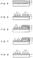
- Fig. 4 is a partial sectional view showing a step of manufacturing the semiconductor device of the present invention;
- Fig. 5 is a partial sectional view showing a step of manufacturing the semiconductor device of the present invention following the step shown in Fig. 4;
- Fig. 6 is a partial sectional view showing a step of manufacturing the semiconductor device of the present invention following the step shown in Fig. 5;
- Fig. 7 is a partial sectional view showing a step of manufacturing the semiconductor device of the present invention following the step shown in Fig. 6; and
- Fig. 8 is a partial sectional view showing a step of manufacturing the semiconductor device of the present invention following the step shown in Fig. 7.
- A semiconductor device according to an embodiment of the present invention will be described below with reference to the accompanying drawings.
- Figs. 4 to 8 are views showing steps of manufacturing a semiconductor device according to an embodiment of the present invention.
- As shown in Fig. 4, an Aℓ-
Cu alloy 3 serving as an electrode wiring line is formed on the surface of asemiconductor substrate 1 through aninsulating film 2. A Cu-basedmaterial 4, e.g., pure Cu is formed on the Aℓ-Cualloy 3. Although film formation is performed by the sputtering method, the deposition method can be used in place of the sputtering method. - As shown in Fig. 5, the resultant structure constituted by stacking the Aℓ-
Cu alloy 3 and the Cu-basedmaterial 4 is formed into electrode wiring lines 3-1 and 3-2. More specifically, the wiring line 3-1 having a size smaller than the crystal grain size of the Aℓ-Cu alloy 3 and the wiring line 3-2 having a size larger than the crystal grain size of the Aℓ-Cu alloy 3 are formed to selectively expose theinsulating film 2. - As shown in Fig. 6, a
resist 5 is covered on a part of the exposed portion of theinsulating film 2, and the Cu-basedmaterial 4. As shown in Fig. 7, the Cu-basedmaterial 4 of the wiring line 3-1 having a size smaller than the crystal grain size of the Aℓ-Cu alloy 3 is selectively removed by exposure and development to expose the thin wiring line 3-1. - On the other hand, the
resist 5 is covered on the thick wiring line 3-2. - As shown in Fig. 8, after the
resist 5 covered on the thick wiring line 3-2 is removed, annealing is performed, e.g., in a reducing atmosphere. As a result, the Cu-basedmaterial 4 of the thick wiring line 3-2 is diffused by using the grain boundaries in the Aℓ-Cu alloy 3 as the main diffusion path to increase the Cu concentration in the Aℓ-Cu alloy 3 of the thick wiring line 3-2. The thick wiring line 3-2 shown in Fig. 8 has a higher Cu concentration than that of the thin wiring line 3-1 by a diffusion amount. - If the Cu concentration of the Aℓ-
Cu alloy 3 in this embodiment is set in advance to be equal to that of the final wiring line 3-1 having a size smaller than the crystal grain size, the resistance to electro-migration of the wiring line 3-1 having a size smaller than the crystal grain size can be maximized, as shown in Fig. 3. - In this case, Cu must not be segregated in the Aℓ-
Cu alloy 3 of the thin wiring line 3-1. Checking the segregated state of Cu, it was confirmed that Cu was not segregated by annealing when the Cu concentration was 0.3 wt% or less. - It was confirmed by experiments that, in the final product, the Cu concentration of the Aℓ alloy wiring line having a size smaller than the crystal grain size was in a range of 0.05 to 0.3 wt%. Also in the Aℓ-
Cu alloy 3 of this embodiment, an optimal resistance to migration was obtained in a range of 0.05 to 0.3 wt% of the Cu concentration. - In the above embodiment, the Cu-based
material 4 is first covered on the Aℓ-Cu alloy 3, and then the resultant structure is formed into the electrode wiring lines. However, the Aℓ-Cu alloy 3 may be first formed into a desired electrode wiring line shape, and the Cu-basedmaterial 4 may be then covered and diffused. - As has been described with reference to Figs. 7 and 8, the Cu-based material is preferably annealed in the reducing atmosphere. However, annealing may be performed in an inert gas atmosphere as of N2 and Ar.
- If annealing was performed in the reducing atmosphere, a Cu oxide film was found to be used as the Cu-based material.
- In the above embodiment, the wiring line 3-2 having a size larger than the crystal grain size can obtain an optimal resistance to electro-migration at the Cu concentration of about 8 wt%. On the other hand, Cu must be segregated at the triple points where the grain boundaries in the Aℓ-Cu alloy 3 overlap. It was confirmed that segregation was caused at the Cu concentration of 0.5 wt% or more by annealing.
- The Cu concentration of 8 wt% or more only causes degradation of the resistance to electro-migration. Therefore, the optimal range of the Cu concentration of the wiring line 3-2 having a size larger than the crystal grain size is defined as 0.5 to 10 wt%.
- The final Cu concentration of the thick wiring line 3-2 can be set by defining the thickness of the Cu-based
material 4 on the basis of the Cu concentration and the thickness of the Aℓ-Cu alloy 3 such that a desired concentration is obtained. - For example, 800-Å pure Cu is covered on a 1-fm thick Aℓ-0.1wt% Cu alloy, and the manufacturing process in Figs. 4 and 5 is performed to obtain a thin wiring line 3-1 having a Cu concentration of 0.1 wt%, and a thick wiring line 3-2 having a Cu concentration of 8 wt%, thereby obtaining an optimal resistance to electro-migration.
- Although the Aℓ-Cu alloy is exemplified as the electrode wiring line, other additive elements containing, e.g., Si may be used to obtain the same effect as described above.
Claims (2)
- A semiconductor device characterized by comprising a wiring line formed from an electrode wiring layer using, as an electrode material, an Aℓ alloy containing Cu, wherein a wiring line (3-1) having a size smaller than a crystal grain size has a Cu concentration of 0.05 to 0.3 wt%, and a wiring line (3-2) having a size larger than a crystal grain size has a Cu concentration of 0.5 to 10 wt%.
- A device according to claim 1, characterized in that said thin and thick wiring lines having different Cu concentrations are formed in a same formation process.
Applications Claiming Priority (3)
| Application Number | Priority Date | Filing Date | Title |
|---|---|---|---|
| JP750593 | 1993-01-20 | ||
| JP7505/93 | 1993-01-20 | ||
| JP750593 | 1993-01-20 |
Publications (3)
| Publication Number | Publication Date |
|---|---|
| EP0609501A2 true EP0609501A2 (en) | 1994-08-10 |
| EP0609501A3 EP0609501A3 (en) | 1994-11-09 |
| EP0609501B1 EP0609501B1 (en) | 1999-09-15 |
Family
ID=11667648
Family Applications (1)
| Application Number | Title | Priority Date | Filing Date |
|---|---|---|---|
| EP19930118141 Expired - Lifetime EP0609501B1 (en) | 1993-01-20 | 1993-11-09 | Aluminium based metallization for semiconductor device |
Country Status (3)
| Country | Link |
|---|---|
| EP (1) | EP0609501B1 (en) |
| KR (1) | KR0131287B1 (en) |
| DE (1) | DE69326432T2 (en) |
Cited By (2)
| Publication number | Priority date | Publication date | Assignee | Title |
|---|---|---|---|---|
| EP0701282A2 (en) * | 1994-08-01 | 1996-03-13 | Motorola, Inc. | Interconnect structure having reduced peak localized current density and method of fabricating an interconnect level in a semiconductor device |
| EP0720219A2 (en) * | 1994-12-30 | 1996-07-03 | AT&T Corp. | Conductive runner fabrication for an integrated circuit |
Citations (1)
| Publication number | Priority date | Publication date | Assignee | Title |
|---|---|---|---|---|
| JPS62114241A (en) * | 1985-11-14 | 1987-05-26 | Fujitsu Ltd | Semiconductor device |
Family Cites Families (1)
| Publication number | Priority date | Publication date | Assignee | Title |
|---|---|---|---|---|
| JPH0284719A (en) * | 1988-09-21 | 1990-03-26 | Nec Corp | Manufacture of semiconductor device |
-
1993
- 1993-11-09 EP EP19930118141 patent/EP0609501B1/en not_active Expired - Lifetime
- 1993-11-09 DE DE1993626432 patent/DE69326432T2/en not_active Expired - Lifetime
-
1994
- 1994-01-19 KR KR1019940000939A patent/KR0131287B1/en not_active IP Right Cessation
Patent Citations (1)
| Publication number | Priority date | Publication date | Assignee | Title |
|---|---|---|---|---|
| JPS62114241A (en) * | 1985-11-14 | 1987-05-26 | Fujitsu Ltd | Semiconductor device |
Non-Patent Citations (4)
| Title |
|---|
| PATENT ABSTRACTS OF JAPAN vol. 11, no. 325 (E-551) 22 October 1987 & JP-A-62 114 241 (FUJITSU LTD) * |
| PATENT ABSTRACTS OF JAPAN vol. 14, no. 268 (E-939) 26 March 1990 & JP-A-02 084 719 (NEC CORP) * |
| PROCEEDINGS OF THE FOURTH INTERNATIONAL IEEE VLSI MULTILEVEL INTERCONNECTION CONFERENCE, June 1987, SANTA CLARA,USA pages 456 - 462 KWOK 'Effects of grain growth and grain structure on electromigration lifetime in Al-Cu submicron interconects' * |
| RELIABILITY PHYSICS, April 1975, LAS VEGAS,USA pages 151 - 158 SCOGGAN ET AL 'Width dependence of electromigratin life in Al-Cu, Al-Cu-Si and Ag conductors' * |
Cited By (5)
| Publication number | Priority date | Publication date | Assignee | Title |
|---|---|---|---|---|
| EP0701282A2 (en) * | 1994-08-01 | 1996-03-13 | Motorola, Inc. | Interconnect structure having reduced peak localized current density and method of fabricating an interconnect level in a semiconductor device |
| EP0701282A3 (en) * | 1994-08-01 | 1996-10-30 | Motorola Inc | Interconnect structure having reduced peak localized current density and method of fabricating an interconnect level in a semiconductor device |
| US5760476A (en) * | 1994-08-01 | 1998-06-02 | Motorola, Inc. | Interconnect run between a first point and a second point in a semiconductor device for reducing electromigration failure |
| EP0720219A2 (en) * | 1994-12-30 | 1996-07-03 | AT&T Corp. | Conductive runner fabrication for an integrated circuit |
| EP0720219A3 (en) * | 1994-12-30 | 1997-05-07 | At & T Corp | Conductive runner fabrication for an integrated circuit |
Also Published As
| Publication number | Publication date |
|---|---|
| EP0609501A3 (en) | 1994-11-09 |
| EP0609501B1 (en) | 1999-09-15 |
| DE69326432T2 (en) | 2000-01-27 |
| KR0131287B1 (en) | 1998-04-14 |
| DE69326432D1 (en) | 1999-10-21 |
Similar Documents
| Publication | Publication Date | Title |
|---|---|---|
| US7247946B2 (en) | On-chip Cu interconnection using 1 to 5 nm thick metal cap | |
| US8053863B2 (en) | Electrical fuse and semiconductor device | |
| EP0843895B1 (en) | Method of manufacturing a metal interconnect structure for an integrated circuit with improved electromigration reliability | |
| EP0751567A2 (en) | Copper alloys for chip and package interconnections and method of making | |
| EP0269211A2 (en) | Semiconductor device having a metallic layer | |
| JPH0652788B2 (en) | Integrated semiconductor circuit | |
| US5567647A (en) | Method for fabricating a gate electrode structure of compound semiconductor device | |
| WO2010143355A1 (en) | Wiring layer structure and process for manufacture thereof | |
| EP0130416B1 (en) | A process for making an ohmic contact to an n-type conductivity group iii-v semiconductor compound and a semiconductor device having such an ohmic contact | |
| US5238874A (en) | Fabrication method for laminated films comprising Al-Si-Co alloy film and refractory metal silioide copper film | |
| US5296406A (en) | Aluminum alloy/silicon-chromium sandwich schottky diode | |
| US4659427A (en) | Via formation for multilayered metalization | |
| US4942451A (en) | Semiconductor device having improved antireflection coating | |
| EP0609501A2 (en) | Aluminium based metallization for semiconductor device | |
| US4502207A (en) | Wiring material for semiconductor device and method for forming wiring pattern therewith | |
| EP0612855A2 (en) | A new compound with room temperature electrical resistivity comparable to that of elemental copper | |
| US5606203A (en) | Semiconductor device having Al-Cu wiring lines where Cu concentration is related to line width | |
| US5260604A (en) | Semiconductor device with improved immunity to contact and conductor defects | |
| JP3333306B2 (en) | Semiconductor device | |
| EP0222795B1 (en) | Polycide process in semiconductor fabrication | |
| Liliental et al. | Electron microscopy study of the AuGe/Ni/Au contacts on GaAs and GaAlAs | |
| EP1001463A2 (en) | Aluminum interconnects for integrated circuits comprising titanium under and overlayers | |
| US5854116A (en) | Semiconductor apparatus | |
| US5461006A (en) | Method for forming contacts with anomalously low resistance | |
| US5565380A (en) | Semiconductor device and process for production thereof |
Legal Events
| Date | Code | Title | Description |
|---|---|---|---|
| PUAI | Public reference made under article 153(3) epc to a published international application that has entered the european phase |
Free format text: ORIGINAL CODE: 0009012 |
|
| 17P | Request for examination filed |
Effective date: 19931109 |
|
| AK | Designated contracting states |
Kind code of ref document: A2 Designated state(s): DE FR GB |
|
| PUAL | Search report despatched |
Free format text: ORIGINAL CODE: 0009013 |
|
| AK | Designated contracting states |
Kind code of ref document: A3 Designated state(s): DE FR GB |
|
| 17Q | First examination report despatched |
Effective date: 19960205 |
|
| GRAG | Despatch of communication of intention to grant |
Free format text: ORIGINAL CODE: EPIDOS AGRA |
|
| GRAG | Despatch of communication of intention to grant |
Free format text: ORIGINAL CODE: EPIDOS AGRA |
|
| GRAH | Despatch of communication of intention to grant a patent |
Free format text: ORIGINAL CODE: EPIDOS IGRA |
|
| GRAH | Despatch of communication of intention to grant a patent |
Free format text: ORIGINAL CODE: EPIDOS IGRA |
|
| GRAA | (expected) grant |
Free format text: ORIGINAL CODE: 0009210 |
|
| AK | Designated contracting states |
Kind code of ref document: B1 Designated state(s): DE FR GB |
|
| REF | Corresponds to: |
Ref document number: 69326432 Country of ref document: DE Date of ref document: 19991021 |
|
| ET | Fr: translation filed | ||
| PLBE | No opposition filed within time limit |
Free format text: ORIGINAL CODE: 0009261 |
|
| STAA | Information on the status of an ep patent application or granted ep patent |
Free format text: STATUS: NO OPPOSITION FILED WITHIN TIME LIMIT |
|
| 26N | No opposition filed | ||
| REG | Reference to a national code |
Ref country code: GB Ref legal event code: IF02 |
|
| PGFP | Annual fee paid to national office [announced via postgrant information from national office to epo] |
Ref country code: FR Payment date: 20101123 Year of fee payment: 18 |
|
| PGFP | Annual fee paid to national office [announced via postgrant information from national office to epo] |
Ref country code: DE Payment date: 20101104 Year of fee payment: 18 |
|
| PGFP | Annual fee paid to national office [announced via postgrant information from national office to epo] |
Ref country code: GB Payment date: 20101103 Year of fee payment: 18 |
|
| GBPC | Gb: european patent ceased through non-payment of renewal fee |
Effective date: 20111109 |
|
| REG | Reference to a national code |
Ref country code: FR Ref legal event code: ST Effective date: 20120731 |
|
| REG | Reference to a national code |
Ref country code: DE Ref legal event code: R119 Ref document number: 69326432 Country of ref document: DE Effective date: 20120601 |
|
| PG25 | Lapsed in a contracting state [announced via postgrant information from national office to epo] |
Ref country code: GB Free format text: LAPSE BECAUSE OF NON-PAYMENT OF DUE FEES Effective date: 20111109 |
|
| PG25 | Lapsed in a contracting state [announced via postgrant information from national office to epo] |
Ref country code: FR Free format text: LAPSE BECAUSE OF NON-PAYMENT OF DUE FEES Effective date: 20111130 |
|
| PG25 | Lapsed in a contracting state [announced via postgrant information from national office to epo] |
Ref country code: DE Free format text: LAPSE BECAUSE OF NON-PAYMENT OF DUE FEES Effective date: 20120601 |