EP0716535A2 - Image sensor and information processing apparatus - Google Patents
Image sensor and information processing apparatus Download PDFInfo
- Publication number
- EP0716535A2 EP0716535A2 EP96100186A EP96100186A EP0716535A2 EP 0716535 A2 EP0716535 A2 EP 0716535A2 EP 96100186 A EP96100186 A EP 96100186A EP 96100186 A EP96100186 A EP 96100186A EP 0716535 A2 EP0716535 A2 EP 0716535A2
- Authority
- EP
- European Patent Office
- Prior art keywords
- image sensor
- supporting member
- original document
- frame
- fixing
- Prior art date
- Legal status (The legal status is an assumption and is not a legal conclusion. Google has not performed a legal analysis and makes no representation as to the accuracy of the status listed.)
- Granted
Links
Images


Classifications
-
- H—ELECTRICITY
- H04—ELECTRIC COMMUNICATION TECHNIQUE
- H04N—PICTORIAL COMMUNICATION, e.g. TELEVISION
- H04N1/00—Scanning, transmission or reproduction of documents or the like, e.g. facsimile transmission; Details thereof
- H04N1/00976—Arrangements for regulating environment, e.g. removing static electricity
-
- H—ELECTRICITY
- H04—ELECTRIC COMMUNICATION TECHNIQUE
- H04N—PICTORIAL COMMUNICATION, e.g. TELEVISION
- H04N1/00—Scanning, transmission or reproduction of documents or the like, e.g. facsimile transmission; Details thereof
- H04N1/024—Details of scanning heads ; Means for illuminating the original
- H04N1/028—Details of scanning heads ; Means for illuminating the original for picture information pick-up
- H04N1/02815—Means for illuminating the original, not specific to a particular type of pick-up head
- H04N1/02845—Means for illuminating the original, not specific to a particular type of pick-up head using an elongated light source, e.g. tubular lamp, LED array
- H04N1/02865—Means for illuminating the original, not specific to a particular type of pick-up head using an elongated light source, e.g. tubular lamp, LED array using an array of light sources or a combination of such arrays, e.g. an LED bar
-
- H—ELECTRICITY
- H04—ELECTRIC COMMUNICATION TECHNIQUE
- H04N—PICTORIAL COMMUNICATION, e.g. TELEVISION
- H04N1/00—Scanning, transmission or reproduction of documents or the like, e.g. facsimile transmission; Details thereof
- H04N1/024—Details of scanning heads ; Means for illuminating the original
- H04N1/028—Details of scanning heads ; Means for illuminating the original for picture information pick-up
- H04N1/03—Details of scanning heads ; Means for illuminating the original for picture information pick-up with photodetectors arranged in a substantially linear array
- H04N1/031—Details of scanning heads ; Means for illuminating the original for picture information pick-up with photodetectors arranged in a substantially linear array the photodetectors having a one-to-one and optically positive correspondence with the scanned picture elements, e.g. linear contact sensors
- H04N1/0311—Details of scanning heads ; Means for illuminating the original for picture information pick-up with photodetectors arranged in a substantially linear array the photodetectors having a one-to-one and optically positive correspondence with the scanned picture elements, e.g. linear contact sensors using an array of elements to project the scanned image elements onto the photodetectors
- H04N1/0312—Details of scanning heads ; Means for illuminating the original for picture information pick-up with photodetectors arranged in a substantially linear array the photodetectors having a one-to-one and optically positive correspondence with the scanned picture elements, e.g. linear contact sensors using an array of elements to project the scanned image elements onto the photodetectors using an array of optical fibres or rod-lenses
-
- H—ELECTRICITY
- H04—ELECTRIC COMMUNICATION TECHNIQUE
- H04N—PICTORIAL COMMUNICATION, e.g. TELEVISION
- H04N1/00—Scanning, transmission or reproduction of documents or the like, e.g. facsimile transmission; Details thereof
- H04N1/024—Details of scanning heads ; Means for illuminating the original
- H04N1/028—Details of scanning heads ; Means for illuminating the original for picture information pick-up
- H04N1/03—Details of scanning heads ; Means for illuminating the original for picture information pick-up with photodetectors arranged in a substantially linear array
- H04N1/031—Details of scanning heads ; Means for illuminating the original for picture information pick-up with photodetectors arranged in a substantially linear array the photodetectors having a one-to-one and optically positive correspondence with the scanned picture elements, e.g. linear contact sensors
- H04N1/0315—Details of scanning heads ; Means for illuminating the original for picture information pick-up with photodetectors arranged in a substantially linear array the photodetectors having a one-to-one and optically positive correspondence with the scanned picture elements, e.g. linear contact sensors using photodetectors and illumination means mounted on separate supports or substrates or mounted in different planes
-
- H—ELECTRICITY
- H04—ELECTRIC COMMUNICATION TECHNIQUE
- H04N—PICTORIAL COMMUNICATION, e.g. TELEVISION
- H04N1/00—Scanning, transmission or reproduction of documents or the like, e.g. facsimile transmission; Details thereof
- H04N1/024—Details of scanning heads ; Means for illuminating the original
- H04N1/028—Details of scanning heads ; Means for illuminating the original for picture information pick-up
- H04N1/03—Details of scanning heads ; Means for illuminating the original for picture information pick-up with photodetectors arranged in a substantially linear array
- H04N1/031—Details of scanning heads ; Means for illuminating the original for picture information pick-up with photodetectors arranged in a substantially linear array the photodetectors having a one-to-one and optically positive correspondence with the scanned picture elements, e.g. linear contact sensors
- H04N1/0318—Integral pick-up heads, i.e. self-contained heads whose basic elements are a light-source, a lens array and a photodetector array which are supported by a single-piece frame
-
- H—ELECTRICITY
- H04—ELECTRIC COMMUNICATION TECHNIQUE
- H04N—PICTORIAL COMMUNICATION, e.g. TELEVISION
- H04N2201/00—Indexing scheme relating to scanning, transmission or reproduction of documents or the like, and to details thereof
- H04N2201/024—Indexing scheme relating to scanning, transmission or reproduction of documents or the like, and to details thereof deleted
- H04N2201/02404—Arrangements for mounting or supporting heads
-
- H—ELECTRICITY
- H04—ELECTRIC COMMUNICATION TECHNIQUE
- H04N—PICTORIAL COMMUNICATION, e.g. TELEVISION
- H04N2201/00—Indexing scheme relating to scanning, transmission or reproduction of documents or the like, and to details thereof
- H04N2201/024—Indexing scheme relating to scanning, transmission or reproduction of documents or the like, and to details thereof deleted
- H04N2201/02406—Arrangements for positioning elements within a head
- H04N2201/02427—Element positioned
- H04N2201/02431—Lens or optical system
-
- H—ELECTRICITY
- H04—ELECTRIC COMMUNICATION TECHNIQUE
- H04N—PICTORIAL COMMUNICATION, e.g. TELEVISION
- H04N2201/00—Indexing scheme relating to scanning, transmission or reproduction of documents or the like, and to details thereof
- H04N2201/024—Indexing scheme relating to scanning, transmission or reproduction of documents or the like, and to details thereof deleted
- H04N2201/02406—Arrangements for positioning elements within a head
- H04N2201/02439—Positioning method
- H04N2201/02441—Positioning method using screws
-
- H—ELECTRICITY
- H04—ELECTRIC COMMUNICATION TECHNIQUE
- H04N—PICTORIAL COMMUNICATION, e.g. TELEVISION
- H04N2201/00—Indexing scheme relating to scanning, transmission or reproduction of documents or the like, and to details thereof
- H04N2201/024—Indexing scheme relating to scanning, transmission or reproduction of documents or the like, and to details thereof deleted
- H04N2201/02452—Arrangements for mounting or supporting elements within a scanning head
- H04N2201/02454—Element mounted or supported
- H04N2201/02456—Scanning element, e.g. CCD array, photodetector
-
- H—ELECTRICITY
- H04—ELECTRIC COMMUNICATION TECHNIQUE
- H04N—PICTORIAL COMMUNICATION, e.g. TELEVISION
- H04N2201/00—Indexing scheme relating to scanning, transmission or reproduction of documents or the like, and to details thereof
- H04N2201/024—Indexing scheme relating to scanning, transmission or reproduction of documents or the like, and to details thereof deleted
- H04N2201/02452—Arrangements for mounting or supporting elements within a scanning head
- H04N2201/02454—Element mounted or supported
- H04N2201/02462—Illuminating means
-
- H—ELECTRICITY
- H04—ELECTRIC COMMUNICATION TECHNIQUE
- H04N—PICTORIAL COMMUNICATION, e.g. TELEVISION
- H04N2201/00—Indexing scheme relating to scanning, transmission or reproduction of documents or the like, and to details thereof
- H04N2201/024—Indexing scheme relating to scanning, transmission or reproduction of documents or the like, and to details thereof deleted
- H04N2201/02452—Arrangements for mounting or supporting elements within a scanning head
- H04N2201/02466—Mounting or supporting method
- H04N2201/02468—Mounting or supporting method using screws
-
- H—ELECTRICITY
- H04—ELECTRIC COMMUNICATION TECHNIQUE
- H04N—PICTORIAL COMMUNICATION, e.g. TELEVISION
- H04N2201/00—Indexing scheme relating to scanning, transmission or reproduction of documents or the like, and to details thereof
- H04N2201/024—Indexing scheme relating to scanning, transmission or reproduction of documents or the like, and to details thereof deleted
- H04N2201/02452—Arrangements for mounting or supporting elements within a scanning head
- H04N2201/02466—Mounting or supporting method
- H04N2201/02474—Clasping; Clamping
-
- H—ELECTRICITY
- H04—ELECTRIC COMMUNICATION TECHNIQUE
- H04N—PICTORIAL COMMUNICATION, e.g. TELEVISION
- H04N2201/00—Indexing scheme relating to scanning, transmission or reproduction of documents or the like, and to details thereof
- H04N2201/024—Indexing scheme relating to scanning, transmission or reproduction of documents or the like, and to details thereof deleted
- H04N2201/02452—Arrangements for mounting or supporting elements within a scanning head
- H04N2201/02479—Mounting or supporting means
- H04N2201/02481—Single piece support, e.g. molded plastic support
-
- H—ELECTRICITY
- H04—ELECTRIC COMMUNICATION TECHNIQUE
- H04N—PICTORIAL COMMUNICATION, e.g. TELEVISION
- H04N2201/00—Indexing scheme relating to scanning, transmission or reproduction of documents or the like, and to details thereof
- H04N2201/024—Indexing scheme relating to scanning, transmission or reproduction of documents or the like, and to details thereof deleted
- H04N2201/02452—Arrangements for mounting or supporting elements within a scanning head
- H04N2201/02479—Mounting or supporting means
- H04N2201/02483—Housing or part of the housing, e.g. bottom plate
-
- H—ELECTRICITY
- H04—ELECTRIC COMMUNICATION TECHNIQUE
- H04N—PICTORIAL COMMUNICATION, e.g. TELEVISION
- H04N2201/00—Indexing scheme relating to scanning, transmission or reproduction of documents or the like, and to details thereof
- H04N2201/024—Indexing scheme relating to scanning, transmission or reproduction of documents or the like, and to details thereof deleted
- H04N2201/028—Indexing scheme relating to scanning, transmission or reproduction of documents or the like, and to details thereof deleted for picture information pick-up
- H04N2201/03—Indexing scheme relating to scanning, transmission or reproduction of documents or the like, and to details thereof deleted for picture information pick-up deleted
- H04N2201/031—Indexing scheme relating to scanning, transmission or reproduction of documents or the like, and to details thereof deleted for picture information pick-up deleted deleted
- H04N2201/03104—Integral pick-up heads, i.e. self-contained heads whose basic elements are a light source, a lens and a photodetector supported by a single-piece frame
- H04N2201/03108—Components of integral heads
- H04N2201/03112—Light source
-
- H—ELECTRICITY
- H04—ELECTRIC COMMUNICATION TECHNIQUE
- H04N—PICTORIAL COMMUNICATION, e.g. TELEVISION
- H04N2201/00—Indexing scheme relating to scanning, transmission or reproduction of documents or the like, and to details thereof
- H04N2201/024—Indexing scheme relating to scanning, transmission or reproduction of documents or the like, and to details thereof deleted
- H04N2201/028—Indexing scheme relating to scanning, transmission or reproduction of documents or the like, and to details thereof deleted for picture information pick-up
- H04N2201/03—Indexing scheme relating to scanning, transmission or reproduction of documents or the like, and to details thereof deleted for picture information pick-up deleted
- H04N2201/031—Indexing scheme relating to scanning, transmission or reproduction of documents or the like, and to details thereof deleted for picture information pick-up deleted deleted
- H04N2201/03104—Integral pick-up heads, i.e. self-contained heads whose basic elements are a light source, a lens and a photodetector supported by a single-piece frame
- H04N2201/03108—Components of integral heads
- H04N2201/03116—Light source lens
-
- H—ELECTRICITY
- H04—ELECTRIC COMMUNICATION TECHNIQUE
- H04N—PICTORIAL COMMUNICATION, e.g. TELEVISION
- H04N2201/00—Indexing scheme relating to scanning, transmission or reproduction of documents or the like, and to details thereof
- H04N2201/024—Indexing scheme relating to scanning, transmission or reproduction of documents or the like, and to details thereof deleted
- H04N2201/028—Indexing scheme relating to scanning, transmission or reproduction of documents or the like, and to details thereof deleted for picture information pick-up
- H04N2201/03—Indexing scheme relating to scanning, transmission or reproduction of documents or the like, and to details thereof deleted for picture information pick-up deleted
- H04N2201/031—Indexing scheme relating to scanning, transmission or reproduction of documents or the like, and to details thereof deleted for picture information pick-up deleted deleted
- H04N2201/03104—Integral pick-up heads, i.e. self-contained heads whose basic elements are a light source, a lens and a photodetector supported by a single-piece frame
- H04N2201/03108—Components of integral heads
- H04N2201/03129—Transparent cover or transparent document support mounted on the head
-
- H—ELECTRICITY
- H04—ELECTRIC COMMUNICATION TECHNIQUE
- H04N—PICTORIAL COMMUNICATION, e.g. TELEVISION
- H04N2201/00—Indexing scheme relating to scanning, transmission or reproduction of documents or the like, and to details thereof
- H04N2201/024—Indexing scheme relating to scanning, transmission or reproduction of documents or the like, and to details thereof deleted
- H04N2201/028—Indexing scheme relating to scanning, transmission or reproduction of documents or the like, and to details thereof deleted for picture information pick-up
- H04N2201/03—Indexing scheme relating to scanning, transmission or reproduction of documents or the like, and to details thereof deleted for picture information pick-up deleted
- H04N2201/031—Indexing scheme relating to scanning, transmission or reproduction of documents or the like, and to details thereof deleted for picture information pick-up deleted deleted
- H04N2201/03104—Integral pick-up heads, i.e. self-contained heads whose basic elements are a light source, a lens and a photodetector supported by a single-piece frame
- H04N2201/03108—Components of integral heads
- H04N2201/03141—Photodetector lens
-
- H—ELECTRICITY
- H04—ELECTRIC COMMUNICATION TECHNIQUE
- H04N—PICTORIAL COMMUNICATION, e.g. TELEVISION
- H04N2201/00—Indexing scheme relating to scanning, transmission or reproduction of documents or the like, and to details thereof
- H04N2201/024—Indexing scheme relating to scanning, transmission or reproduction of documents or the like, and to details thereof deleted
- H04N2201/028—Indexing scheme relating to scanning, transmission or reproduction of documents or the like, and to details thereof deleted for picture information pick-up
- H04N2201/03—Indexing scheme relating to scanning, transmission or reproduction of documents or the like, and to details thereof deleted for picture information pick-up deleted
- H04N2201/031—Indexing scheme relating to scanning, transmission or reproduction of documents or the like, and to details thereof deleted for picture information pick-up deleted deleted
- H04N2201/03104—Integral pick-up heads, i.e. self-contained heads whose basic elements are a light source, a lens and a photodetector supported by a single-piece frame
- H04N2201/03108—Components of integral heads
- H04N2201/03145—Photodetector
-
- H—ELECTRICITY
- H04—ELECTRIC COMMUNICATION TECHNIQUE
- H04N—PICTORIAL COMMUNICATION, e.g. TELEVISION
- H04N2201/00—Indexing scheme relating to scanning, transmission or reproduction of documents or the like, and to details thereof
- H04N2201/024—Indexing scheme relating to scanning, transmission or reproduction of documents or the like, and to details thereof deleted
- H04N2201/028—Indexing scheme relating to scanning, transmission or reproduction of documents or the like, and to details thereof deleted for picture information pick-up
- H04N2201/03—Indexing scheme relating to scanning, transmission or reproduction of documents or the like, and to details thereof deleted for picture information pick-up deleted
- H04N2201/031—Indexing scheme relating to scanning, transmission or reproduction of documents or the like, and to details thereof deleted for picture information pick-up deleted deleted
- H04N2201/03104—Integral pick-up heads, i.e. self-contained heads whose basic elements are a light source, a lens and a photodetector supported by a single-piece frame
- H04N2201/0315—Details of integral heads not otherwise provided for
- H04N2201/03158—Heat radiator
-
- H—ELECTRICITY
- H04—ELECTRIC COMMUNICATION TECHNIQUE
- H04N—PICTORIAL COMMUNICATION, e.g. TELEVISION
- H04N2201/00—Indexing scheme relating to scanning, transmission or reproduction of documents or the like, and to details thereof
- H04N2201/024—Indexing scheme relating to scanning, transmission or reproduction of documents or the like, and to details thereof deleted
- H04N2201/028—Indexing scheme relating to scanning, transmission or reproduction of documents or the like, and to details thereof deleted for picture information pick-up
- H04N2201/03—Indexing scheme relating to scanning, transmission or reproduction of documents or the like, and to details thereof deleted for picture information pick-up deleted
- H04N2201/031—Indexing scheme relating to scanning, transmission or reproduction of documents or the like, and to details thereof deleted for picture information pick-up deleted deleted
- H04N2201/03104—Integral pick-up heads, i.e. self-contained heads whose basic elements are a light source, a lens and a photodetector supported by a single-piece frame
- H04N2201/0315—Details of integral heads not otherwise provided for
- H04N2201/03162—Original guide plate
-
- H—ELECTRICITY
- H04—ELECTRIC COMMUNICATION TECHNIQUE
- H04N—PICTORIAL COMMUNICATION, e.g. TELEVISION
- H04N2201/00—Indexing scheme relating to scanning, transmission or reproduction of documents or the like, and to details thereof
- H04N2201/024—Indexing scheme relating to scanning, transmission or reproduction of documents or the like, and to details thereof deleted
- H04N2201/028—Indexing scheme relating to scanning, transmission or reproduction of documents or the like, and to details thereof deleted for picture information pick-up
- H04N2201/03—Indexing scheme relating to scanning, transmission or reproduction of documents or the like, and to details thereof deleted for picture information pick-up deleted
- H04N2201/031—Indexing scheme relating to scanning, transmission or reproduction of documents or the like, and to details thereof deleted for picture information pick-up deleted deleted
- H04N2201/03104—Integral pick-up heads, i.e. self-contained heads whose basic elements are a light source, a lens and a photodetector supported by a single-piece frame
- H04N2201/0315—Details of integral heads not otherwise provided for
- H04N2201/0317—Shape
-
- H—ELECTRICITY
- H04—ELECTRIC COMMUNICATION TECHNIQUE
- H04N—PICTORIAL COMMUNICATION, e.g. TELEVISION
- H04N2201/00—Indexing scheme relating to scanning, transmission or reproduction of documents or the like, and to details thereof
- H04N2201/04—Scanning arrangements
- H04N2201/047—Detection, control or error compensation of scanning velocity or position
- H04N2201/04753—Control or error compensation of scanning position or velocity
- H04N2201/04794—Varying the control or compensation during the scan, e.g. using continuous feedback or from line to line
- H04N2201/04796—Varying the sub-scan control during the main-scan, e.g. for correcting skew, tilt or bow of a scanning beam
Abstract
Description
- The present invention relates to an information processing apparatus on which a contact type image sensor for use in an image reader, a facsimile machine or the like is mounted. More particularly, the present invention relates to an improvement in the composition of parts of the above-described contact type image sensor.
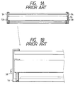
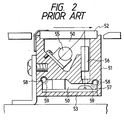
- Fig. 1A is a schematic side elevational view which illustrates a conventional contact type image sensor. Fig. 1B is a partial enlarged view of the same. Fig. 2 is a schematic structural view which illustrates the image sensor mounted on the body of the apparatus. As shown in Figs. 1 and 2, the conventional contact type image sensor is arranged in such a manner that one
hollow portion 50 is created by aframe 51, areading glass 52, abottom plate 53,side plates 54 and the like. Furthermore, optical elements, such as anLED array 55, a SELFOClens 56 and asensor substrate 57, are accommodated in the above-describedhollow portion 50. - However, in the above-described conventional structure, the leading portions of
screws 58 for use in assembling the elements undesirable appear in thehollow portion 50 in which the optical elements are accommodated. Therefore,chips 59 genenerated in a tap portion at the time of tightening thescrew 58 are undesirably introduced into the above-describedhollow portion 50. As a result, thechips 59 will adhere to the open side of the lens, the reverse side of the reading glass and the surfaces of the sensor devices and the like and thereby the image is adversely critically influenced. The above-described problem becomes seriously in a case where the contact type image sensor has an improved reading resolution because a small chip will adversely affect the quality of the formed image. - The oxidation and optically adverse influence upon the
frame 51 have been prevented by applying a black insulating material to the surface of theframe 51 after theframe 51 has been formed into the final shape. Therefore, no electrical connection has not been established between the above-describedframe 51 and thebottom plate 53 and theside plates 54 which accommodate the optical elements. - As a result, although the above-described
bottom plate 53 and theside plates 54 are disposed to surround the above-describedframe 51, the force to shield electric waves becomes insufficient and an undesirable antenna effect is generated, causing the following problems to take place in a case where the contact type image sensor is, as described above, mounted on an apparatus such as an image reader. - That is, it is difficult, for the structure composed of the
frame 51, thebottom plate 53 and theside plates 54 to confine the electric waves which have been generated in thesensor substrate 57 when the contact type image sensor is operated. As a result, the radiant noise characteristics will be deteriorated because the electric waves can easily leak outside. Because of the same reason, the force to shield the electric waves made incident from the external portion of the contact type image sensor is insufficient. Therefore, the contact type image sensor cannot be operated stably. In order to overcome the above-described problems, it might be feasible to employ a structure arranged in such a manner that a large quantity of the ground wires are used or an electric wave shield tape is used. However, the overall cost will be enlarged excessively in this case. - The above-described problems become more seriously in a case where the regulation of radiant noise, which has been intensified recently, must be met or when the apparatus is arranged to adapt to the electric waves the frequency of which has been raised or strengthened and to take a measurement against the deterioration in the resistance against external noise which will be taken place when the speed of the operational clock of the contact type image sensor is raised in order to improve the reading resolution and to raise the reading speed.
- Furthermore, since the
LED array 55, which is the heat generation source, is usually disposed adjacent to the central portion of theframe 51, it is difficult to satisfactorily discharge the accumulated inside heat. - It becomes more difficult to overcome the above-described problem of the heat radiation in a case of a small apparatus. Furthermore, if the reading resolution of a document reading apparatus is desired to be improved or its speed is intended to be raised, a strong light source must be used, causing a serious problem to arise in that the calorific power is excessively enlarged.
- An object of the present invention is to prevent a malfunction of an image sensor by improving the structure of a supporting member and thereby improving the reliability of the image sensor.
- Another object of the present invention is to provide an image sensor having a supporting member for integrally supporting a reading system including illuminating means for illuminating an original document, a photoelectrically converting means and imaging means for imaging light reflected by the surface of the original document onto the photoelectrically converting means, and having a member for converting the side surface of the supporting member, wherein the image sensor comprising: two or more substantially independent spaces formed in the supporting member, and wherein the illuminating means, the imaging means and the photoelectrically converting means are accommodated in one of the spaces and to as well provide an information processing apparatus on which the image sensor is mounted.
- Another object of the present invention is to provide an image sensor comprising: illuminating means for illuminating an image information surface of an original document; imaging means for imaging light reflected from the image information surface of the original document by the illuminating means; a light receiving device disposed on the image surface of the reflected light, arranged to photoelectrically convert the reflected light and arranged to receive image information; a supporting member for integrally holding the illuminating means, the imaging means and the light receiving device; and means for fixing the supporting member, wherein the supporting member is made of an electrically conductive material, an insulating film is formed on the surface of the supporting member, at least the surface of the fixing member is made of an electrically conductive material and the supporting member and the fixing member are secured in such a manner that an electrical conduction is established between the supporting member and the fixing member and to as well as provide an information processing apparatus.
- Another object of the present invention to provide an image sensor comprising two or more independent hollow portions formed in a supporting member, wherein all of optical elements such as illuminating means, imaging means and light receiving device are accommodated in one of the independent hollow portions and at least one of the side plate portions of the hollow portion except for the hollow portion which accommodates the optical elements are opened outside and to as well as provide an image processing apparatus.
- Other and further objects, features and advantages of the invention will be appear more fully from the following description.
-
- Figs. 1A and 1B are schematic views which illustrates a conventional image sensor;
- Fig. 2 is a schematic cross sectional view which illustrates the conventional image sensor;
- Figs. 3A and 3B are schematic views which illustrates a first embodiment of an image sensor according to the present invention;
- Fig. 4 is a schematic cross sectional view which illustrates the first embodiment of the image sensor according to the present invention;
- Figs. 5, 6 and 7 are schematic cross sectional views which illustrate other embodiments of the image sensor according to the present invention;
- Fig. 8 is a schematic view which illustrates a method of covering a gap between a connection cable and a hole;
- Fig. 9 is a schematic cross sectional view which illustrates an information processing apparatus according to the present invention;
- Fig. 10A is a front elevational view which illustrates a second embodiment of the image sensor according to the present invention;
- Fig. 10B is an enlarged front elevational view which illustrates an essential portion of the same;
- Fig. 11 is a schematic cross sectional view which illustrates the second embodiment of the image sensor according to the present invention;
- Fig. 12A is a schematic view which illustrates the sequential order of an alumite treatment process;
- Fig. 12B is a schematic view which illustrates the sequential order of a tapping process;
- Fig. 13 is a scheamtic view which illustrates a sequential order of a process of causing the basic surface which is not applied with an alumite coating to appear;
- Fig. 14 is a schematic view which illustrates another sequential order of a process of causing the basic surface which is not applied with an alumite coating to appear;
- Fig. 15 is a schematic cross sectional view which illustrates a third embodiment of the image sensor according to the present invention;
- Figs. 16A and 16B are schematic views which illustrates the third embodiment of the image sensor according to the present invention;
- Figs. 17A and 17B schematic views which illustrates the third embodiment of the image sensor according to the present invention;
- Fig. 18 is a schematic view which illustrates another embodiment of the image sensor according to the present invention; and
- Figs. 19A and 19B schematic views which illustrates another embodiment of the image sensor according to the present invention.
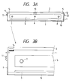
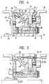
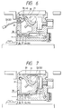
- Fig. 3 is a schematic view which illustrates a first embodiment of a contact type image sensor according to the present invention. Fig. 3A is an overall view of the same and Fig. 3B is an enlarged view which illustrates a portion including a side plate. Fig. 4 is a side elevational schematic cross sectional view which illustrates the contact type image sensor. Referring to Figs. 3 and 4,
reference numeral 1 represents a frame serving as a supporting member, 2 represents a reading glass. Asensor substrate 3 and asensor device 4 constitute a photoelectrical conversion means.Reference numeral 5 represents a SELFOC lens serving as an imaging means.Reference numerals Reference numerals Reference numeral 23 represents a fastening plate, 24 represents a fastening/fixing screw, 25 represents a fastening plate side original document guide and 26 represents a lens side original document guide.Reference numeral 17 represents an apparatus body, 28 represents a contact type image sensor fixing screw and 29 represents an original document. The basic reading system is composed of a photoelectrical conversion means, an imaging means and an illuminating means. - The
frame 1 is formed into the final shape by cutting an extruded aluminum-alloy workpieces and as well as the entire surface of same is subjected to a black alumite treatment in order to prevent an adverse influence upon the internal optical system and undesirable change of the state of the surface thereof. - The reading
glass 2 is chamferred on its original document introduction side so as to prevent undesirable catch of the original document. - On the
sensor substrate 3,sensor devices 4 such as a photoelectrical conversion device, a photoconductive device, a photoelectromotive device are mounted. - The
SELFOC lens 5 is secured to theframe 1 by thelens fixing screws - The
side plates frame 1 by the corresponding sideplate fixing screws - The reading
glass 2 is, by the reading glass adhesion layers 13, 14 and 15, secured to the central portion, theside plates frame 1. - The
bottom plate 16 is formed into the final shape by cutting an extruded aluminum-alloy workpiece and as well as the entire surface of same is subjected to a black alumite treatment in order to prevent undesirable change of the state of the surface thereof. Furthermore, thebottom plate 16 is secured to theframe 1 by the bottomplate fixing screws rubber shafts bottom plate 16 by adhesion or the like so that thesensor substrate 3 is fixed by the pressing force. - The
LED array 21 is constituted in such a manner that an LED chip, a cylindrical lens and the like are mounted on the substrate and the same is secured to theframe 1 by the LEDarray fixing screw 22. - The
fastening plate 23 is made of sheet metal and the same is fixed to theframe 1 by the fasteningplate fixing screw 24. The contact type image sensor is, via thefastening plate 23, secured to theapparatus body 27 by the contact-type imagesensor fixing screw 28. - According to this embodiment, the fastening plate side
original document guide 25 is formed into a guide plate to smoothly introduce the original document onto the readingglass 2, the fastening plate sideorignal document guide 25 being secured to theapparatus body 27. - According to this embodiment, the lens side
original document guide 26 is formed into a guide plate to smoothly discharge the original document from the readingglass 2, the lens sideoriginal document guide 26 being secured to theapparatus body 27. - The
original document 29 is smoothly introduced onto the readingglass 2 along the fastening plate sideoriginal document guide 25, while the same is smoothly discharged from the readingglass 2 along the lens sideoriginal document guide 26. At this time, the surface of theoriginal document 29 confronting thereading glass 2 is illuminated on thereading glass 2 by a light beam emitted from theLED array 21. As a result, the image of theoriginal document 29 is imaged on thesensor device 4 by theSELFOC lens 5. The image is then photoelectrically converted by thesensor device 4 before it is amplified on thesensor substrate 3 so as to be transmitted to outside of the contact type image sensor. - The
frame 1 includes independent space, that is,hollow portions hollow portion 30 is a space defined by theframe 1, the readingglass 2, theside plates bottom plate 16. Thehollow portion 31 is a space defined by theframe 1, theside plates hollow portions hollow portions - The
hollow portion 30 accommodates all of the essential optical elements such as thesensor substrate 3, theSELFOC lens 5, thebottom plate 16 and theLED array 21. - On the other hand, the
hollow portion 31 does not accommodate the optical elements. - All of the screws for use in building up the contact type image sensor except for the
lens fixing screws hollow portion 31. The reason for arranging the screws in the above-described manner lies in that the tapping work can easily be performed, the necessity of improving the dimensional accuracy of the screw length can be eliminated and the introduction of dust generated at the time of tightening the screws into the screw head portion can be prevented. The above-described structure is suitable when the LEDarray fixing screw 22, the head portion of which projects into thehollow portion 30, is used. - Since the structure is arranged as described above, the leading portion of the screws for use in building up the contact type image sensor, and, more particularly, the same of the screws to be tightened toward the inside portion of the
frame 1 and those disposed in theframe 1 do not appear in thehollow portion 30 which accommodates the optical elements. As a result, the undesirable introduction of the chips generated from the tapped portion into thehollow portion 30 can be prevented and thereby the image can be satisfactorily protected from an adverse influence. - According to this embodiment, the
SELFOC lens 5 is arranged to be fixed by screws. Therefore, there is a risk of the introduction of the chips generated from the tapped portions of thelens fixing screws hollow portion 30 when theSELFOC lens 5 is secured. Therefore, the tapped portion of thelens fixing screws screws elastic sealant 32 before theSELFOC lens 5 is secured by them. Theelastic sealant 32 according to this embodiment is a gap filler such as silicon rubber type filler. - As described above, the
elastic sealant 32 is applied to the screws or the tapped portions so that the undesirable introduction of the chips into thehollow portion 30 can be prevented even if the leading portions of the screws appear in thehollow portion 30. Therefore, even if another structure is employed in which the leading portions of the screws except for the screws for fixing the lens for use in building up the contact type image sensor are allowed to appear in thehollow portion 30, the deterioration of the image taken place due to the chips can be prevented. However, it is preferable that the structure be arranged as described above in such a manner that the leading portions of the screws for use in building up the contact type image sensor do not appear in thehollow portion 30 in order to reduce the overall cost by preventing an increase in the number of the manufacturing processes required to apply theelastic sealant 32. - Furthermore, if a structure is employed in such a manner that the
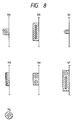
SELFOC lens 5 is secured by an adhesive to eliminate the necessity of fixing theSELFOC lens 5 from outside, the above-described problem can be overcome and thereby theelastic sealant 32 can be omitted from the structure. - In order to operate the contact type image sensor, the optical elements included by the contact type image sensor and the outer portion of the contact type image sensor must be connected to one another by elements. Figs. 5, 6 and 7 are perspective views which illustrate a portion including the side plate of the contact type image sensor.
- In order to cause the
LED array 21 serving as the illuminating means to emit light, electrical energy must be supplied to theLED array 21 from outside. Therefore, electric power is supplied from outside by using an LEDpower supply cable 33, the LEDpower supply cable 33 being allowed to comprise an ordinary cable having a circular cross sectional shape. In a case where the illuminating means is arranged to perform the illumination by using, for example, external light in place of theLED array 21, a light supply means such as an optical fiber must be used. Furthermore, electric power, control signals, and read image signals must be transmitted via asensor substrate cable 34 in order operate the sensor, which is the light receiving device, and outwards transmit a read image information signal. Thesensor substrate cable 34 may comprise a flexible substrate or a flat cable. - The above-described elements serving as the connecting members are collectively called a connecting
cable 35 hereinafter. - The connecting
cable 35 is connected to outside portion of the contact type image sensor after it has passed through holes formed in theframe 1, theside plates bottom plate 16 and the like. According to this embodiment, thehole 36 is formed by a groove created by secondarily processing theframe 1 and theside plates bottom plate 16 in order to easily cause the connectingcable 35 to pass through. If there is agap 37 between the connectingcable 35 and thehole 36, there is a risk of introduction of foreign matter such as chips or dust through thegap 37 into thehollow portion 30 which accommodates the optical elements, causing the image to be adversely influenced. Therefore, it is preferable that the number of theholes 36 be reduced. This will cause another effect to be obtained in that the cost can be reduced since the number of portions which must be subjected to the secondary process can be decreased. The problem of the undesirable introduction of the chips and dust through thegaps 37 between the connectingcables 35 and theholes 36, the number of each of which is reduced can be overcome by sealing thegaps 37 by a sealingmember 38. - In order to decrease the number of the
holes 36, the structure must be arranged in such a manner that the connectingcable 36 does not pass through thehollow portion 31, which does not accommodate the optical elements but the same directly appear outside from thehollow portion 30. In a case where a plurality of the connectingcables 35 such as the above-described LEDpower supply cable 33 and thesensor substrate cable 34 are used, a plurality of the cables are collectively pulled out through onehole 36 as illustrated. Thus, the number of thehole 36 can be minimized and thereby the cost can be reduced. - However, there is a case in which the connecting
cable 35 must pass through thehollow portion 31 due to the necessity of the internal space depending upon the structure of the contact type image sensor or a direction through which the connectingcable 35 appear outside from the contact type image sensor. In this case, a plurality ofholes 39 and 40 through which the connecting cables pass through must be used. However, it is able to prevent the introduction of dust into thehollow portion 30 while eliminating the necessity of increasing the number of the sealingmembers 38 by providing the sealingmembers 38 for only the holes 39 which establishes the connection between the twohollow portions - The
gap 37 can be sealed by a variety of methods as shown in Fig. 8. - A method designated by symbol 4a may be employed in which the portion around the connecting
cable 35 having a circular cross section is surrounded by the sealingmember 38. Another method designated by symbol 4b may be employed in which the connectingcable 35 of a flat type is surrounded by the sealingmember 38. Another method designate by symbol 4c may be employed in which the connectingcable 35 having a circular cross section is brought into contact with either side of thehole 36 and the residual space is filled with the sealingmember 38. - Another method designated by symbol 4d may be employed in which the flat
type connecting cable 35 is brought into contact with either side of thehole 36 and the residual space is filled with the sealingmember 38. Another method may be employed in which a plurality of the connectingcable 35 each having a circular cross section are provided. Another method may be employed in which the connectingcable 35 having a circular cross section and the flattype connecting cable 35 are combined with each other. - In a case where the
hole 36 is not disposed between the two elements, the shape becomes as designated by symbol 4g. - The present invention is not limited to the above-described methods of sealing the
gap 37. They may be arbitrarily combined with each other or the shape may be modified. In addition, the number of the connectingcables 35 is not limited particularly. Furthermore, it is preferable that the sealingmember 38 be made of an elastic sealant or an elastic material such as rubber and formed by injection molding. However, material which is hardened after the solidification such as an adhesive may be employed. - Although the above-described embodiment is arranged in such a manner that the two independent hollow portions are formed in the contact type image sensor, it may be modified properly within the scope of the present invention. For example, three or more hollow portions may be formed.
- It is preferable that the
optical sensor 4 comprises an elongated optical sensor of the type which is composed of amorphous silicone and which is disclosed in U.S.P. 4,461,956 granted to Hatanaka and the like; the inventor of the present invention because its cost can be reduced and an excellent resolution can be obtained. - Also an optical sensor of a type disclosed in U.S.P. 4,791,469 granted to Omi; the inventor of the present invention or that disclosed in U.S.P 4,810,896 granted to Tanaka; the inventor of the present invention may be employed which is arranged in such a manner that a capacity load is provided for the emitter of a bipolar transistor and an output signal is read by means of voltage. In this case, a plurality of sensor chips are straight or in a zigzag manner disposed on the surface of the ceramic substrate and the same is subjected to passivation by silicone resin or the like.
- Fig. 9 illustrates an example of a facsimile machine serving as an image information apparatus constituted by using the sensor unit according to this embodiment and having a communication function. Referring to Fig. 9,
reference numeral 102 represents a supplying roller serving as a supply means for supplying original document OR toward a reading position.Reference numeral 104 represents a separating member for assuredly and one by one separating and supplying the original document OR.Reference numeral 106 represents a platen roller serving as a conveying means disposed at the reading position with respect to the sensor unit and arranged to restrict the surface of the original document OR to be read and as well as convey the original document OR. - Symbol P represents a recording medium formed into a roll of paper in which image information transmitted from outside is reproduced in a case of image information read by the sensor unit or in a case of a facsimile machine.
Reference numeral 110 represents a recording head serving as a recording means for forming the above-described image, the recording head being allowed to comprise a variety of heads such as a thermal head and an ink jet recording head. The recording head according to this embodiment may comprise a serial type recording head or line type recording head.Reference numeral 112 represents a platen roller serving as a conveying means for conveying the recording medium P to the recording position made by therecording head 110 and as well as restricting the surface of the recording medium P to be recorded. -
Reference numeral 120 represents an operation panel serving as an input/output means on which switches for receiving operational inputs and display portions for displaying messages and information about the states of the apparatus are disposed. -
Reference numeral 130 represents a system control substrate serving as a control means and comprising a control portion (controller) for controlling the operation of each unit, a drive circuit (driver) for driving the photoelectrical conversion device, a processing portion (processor) for processing image information and information transmitting/receiving portion and the like.Reference numeral 140 represents a power source for the apparatus. - It is preferable that the recording means for use in the information processing apparatus according to the present invention comprises a means the representative structure and the principle of which have been disclosed in U.S.P.4,723,129 or U.S.P. 4,740,796. According to these disclosures, one or more drive signals which correspond to information to be recorded and which cause a rapid temperature rise exceeding nuclear boiling are supplied to an electrothermal converter which is disposed to correspond to a sheet or a liquid passage in which liquid (ink) is held. As a result, thermal energy is generated in the electrothermal converter, causing film boiling to be generated in the heat effective surface of the recording head. Consequently, bubbles can be formed in liquid (ink), one by one, corresponding to the drive signals, causing a significant effect to be obtained. When the bubbles are enlarged/contracted, liquid (ink) is discharged through discharge apertures so that one or more droplet are formed.
- Furthermore, in a case where the recording head is a full line type recording head having a length which corresponds to the maximum width of the recording medium which can be recorded by the recording apparatus, a structure may be employed in which a plurality of recording heads disclosed in the above-described disclosures are combined with each other to correspond to the above-described length. Another structure may be employed which has a single recording head constituted by integrating a plurality of heads.
- Furthermore, the present invention can be effectively adapted to an interchangeable chip-type recording head which is arranged in such a manner that, when it is mounted on the apparatus body, an electrical connection with the apparatus body or ink supplied from the apparatus body can be enabled. In addition, the present invention can be effectively adapted to a cartridge type recording head in which an ink tank is integrally provided for the body of the recording head.
- As described above, according to this embodiment, a contact type image sensor is arranged in such a manner that two or more independent hollow portions are formed in the frame and all of the optical elements such as the illuminating means, the imaging means and the light receiving devices and the like are accommodated in one of the hollow portions. The leading portions of the screws do not appear in the accommodating portion which accommodates the optical elements at the time of assembling the contact type image sensor. Therefore, the deterioration in the image quality can be prevented, the deterioration being due to the introduction of the chip generated in the tapping operation into the accommodating portion which accommodates the optical elements.
- Referring to Figs. 10A, 10B and 11,
reference numeral 1 represents a frame of a contact type image sensor to which the following elements are fastened: a readingglass 2, asensor substrate 3 having asensor device 4 serving as the light receiving device, aSELFOC lens 5 serving as an imaging means,side plates bottom plate 16 which are secured to the above-describedframe 1 and anLED array 21 serving as the illuminating means. According to this embodiment, the above-describedSELFOC lens 5 is secured bylens fixing screws side plates plate fixing screws bottom plate 16 is secured by bottomplate fixing screws sensor substrate 3 is, via sensor substrate fixingrubber shafts frame 1 and thebottom plate 16. In addition, theLED array 21 is secured by an LEDarray fixing screw 22. Theframe 1 is secured to afastening plate 23 by a fasteningplate fixing screw 24, while thefastening plate 23 is secured to anapparatus body 27 by a contact-type imagesensor fixing screw 28.Reference numeral 25 represents a fastening plate side original document guide, 26 represents a lens side original document guide and 29 represents an original document. - The above-described
frame 1 is formed into its final shape by subjecting an extruded aluminum workpiece to a secondary machining such as a cutting work. In order to prevent the adverse influence upon the internal optical system and preventing the surface oxidation, it subjected to the black alumite treatment. As a result, a non-conductive film is formed on the surface of theframe 1. - The reading
glass 2 is chamfered on its original document introduction side so as to prevent the undesirable check of the original document. Theside plates side plates frame 1 by the sideplate fixing screws glass 2 is secured to the central portion of theframe 1, theside plates bottom plate 16 is formed into its final shape by cutting the extruded aluminum workpiece and the same is subjected to the alumite treatment in order to prevent the change in the surface condition such as oxidation. - The
LED array 21 has a substrate on which an LED chip, a cylindrical lens and the like are mounted. Thefastening plate 23 is a steel sheet which is applied with a surface treatment such as nickel plating, tin plating, aluminum plate or the like exhibiting excellent high frequency conductivity in order to prevent the surface condition change such as oxidation and as well as to improve the electrical conductivity. - According to this embodiment, the fastening plate side
original document guide 25 serves as a guide plate for smoothly introducing the original document onto the surface of the readingglass 2, the fastening plate sideoriginal document guide 25 being secured to theapparatus body 27. The above-described lens sideoriginal document guide 26 is, according to this embodiment, arranged to be a guide plate for smoothly discharging the original document from the readingglass 2, the lens side original document guide being secured to theapparatus body 27. - The
original document 29 is smoothly introduced onto the surface of the readingglass 2 along the fastening plate sideoriginal document guide 25, while the same is discharged from the readingglass 2 along the lens sideoriginal document guide 26. At this time, the surface of theoriginal document 29 confronting thereading glass 2 is, on thereading glass 2, illuminated by the light beams emitted from the LED array. As a result, an image written on theoriginal document 29 is imaged on thesensor device 4 by theSELFOC lens 5. Thus, the image is photoelectrically converted by thesensor device 4 before it is amplified on thesensor substrate 3 so as to be transmitted outside of the contact type image sensor. - Since the above-described
side plates plate fixing screws side plates frame 1 are made of steel and the same is applied with nickel plating which exhibits excellent electrical conductivity. Since theprimary hole 30 for tapping and athread hole 31 are usually formed in theframe 1 before the alumite treatment is performed, the electrically conductive state is not realized even if screws are directly fastened. According to this embodiment, the tappingprimary hole 30 is formed in theframe 1 as shown in Fig. 12B before the alumite treatment is performed. Then, tapping of theframe 1 is performed so that the alumite film is removed in thethread hole 31. As described above, according to this embodiment, an effect can be obtained in that the overall cost can be reduced because the tapping process is arranged to be performed after the alumite treatment in order to establish the electrical conduction. - When screw fixing is performed as described above, an electrical conduction can be established between the
frame 1 and the side plates via the sideplate fixing screws plate fixing screws frame 1 and theside plates frame 1 must be arranged in such a manner that the base surface having electrical conductivity must appear in place of the alumite film. The base surface can be allowed to appear outside by the following means:
A means shown in Fig. 13 is arranged in such a manner that theframe 1 is first subjected to the alumite treatment before the alumite film is removed in the required portions by a secondary machining. The above-described secondary machining process may comprise a milling process. Furthermore, the removal of the alumite film by tapping as described above is a kind of the secondary machining process. - The above-described machining is characterized by a fact that the shape of the portion in which the base surface is caused to appear outside is changed. Therefore, if the base surface of the subject portion can be caused to appear outside by another secondary machining process performed for another purpose, any special process for causing the base surface to appear outside according to the present invention can be omitted.
- A means shown in Fig. 4 is arranged in such a manner that no alumite film is formed in the required portions at the time of the alumite treatment. That is, masking is previously applied to the portion of the
frame 1 the base surface of which must appear outside. Then, the mask is removed after the alumite treatment has been completed. As a result, the base surface of the required portion, to which no alumite treatment is applied, appear outside. The above-described masking process is performed by applying a resist or by using a masking tape each of which is not influenced by the alumite treatment. - The above-described machining is characterized in that the shape of the portion, the base surface of which is caused to appear outside, is not changed. Furthermore, an excellent effect can be obtained if it is used to cause a wide area to appear outside.
- In any of the above-described machining means, an excellent effect can be obtained in the portion which receives pressure at the time of tightening the screw. That is, the portion around the tapped portion according to this embodiment. It is preferable that the exposed area be wide within the contact surface, more preferably, an area larger than the screw seat contact area.
- According to this embodiment, since the
bottom plate 16 is made of an aluminum alloy similarly to theframe 1, therefore there is no electrical conductivity. In this case, the bottomplate fixing screws frame 1 is subjected to the alumite treatment after the tapping primary hole has been formed therein. Then, tapping of the tapping primary hole is performed. As a result, the alumite film on theframe 1 is removed in the tappedportions bottom plate 16 and the seating surfaces of the bottomplate fixing screws reference numerals 36 and 37) is performed in thebottom plate 16 after the overall alumite treatment has been performed in order to cause the base surface to appear outside. As a result, an electrical conduction is established between theframe 1 and thebottom plate 16 via the seatingsurface contact portions plate fixing screws portions plate fixing screws bottom plate 16 can be eliminated, a masking treatment applied to the subject portion to cause the base surface to appear outside later is employed in place of the counterboring so as to establish the electrical conduction. - In a case where the conductivity established by the bottom
plate fixing screws bottom plate 16 and thecontact surface 38 to increase the electrically conductive area. In this case, the surface at which theframe 1 and the bottom plate are positioned in contact with each other must be arranged in such a manner that its base surface having electrical conductivity must appear outside by removing the alumite film. - As described above, any one of the above-described means may be employed to cause the base surface to appear outside. An excellent effect can be obtained from the fact that the base surface appears outside in the portion which receives the pressure at the time of tightening the screw. Also according to this embodiment, it is preferable that the exposure range be wide within the contact surface. According to this embodiment, the surface of the
fastening plate 23 has electrical conductivity. The means for fastening thefastening plate 23 to theframe 1 is arranged to be similar to the above-described embodiment. The lens fixing screws 6, 7 and 8 for securing elements having no electrical conductivity may be subjected to proper machining/processing order in terms of convenience in manufacturing the contact type image sensor because the sequential order of the non-conductive film forming process and the tapping process may be arbitrarily determined. - According to the above-described embodiments, the side plates are made of stainless steel, the screws are made of steel and the fastening plate is made of a steel plate applied with electrically conductive plating. However, the above-described material may be changed if the surface of the element has the electrical conductivity. For example, the side plate may be made of a steel plate applied with electrically conductive plating and the screws and the fastening plate respectively may be made of stainless steel. As an alternative to this, they may be made of copper or another metal material. Furthermore, a plastic material possessing electrical conductivity because copper dust or carbon dust are mixed may be employed. In addition, a non-conductive plastic applied with electrical conductive plating such as nickel plating may be employed.
- Furthermore, the frame may be made of any electrical conductive material in place of the aluminum alloy. In addition, the film on the surface may be formed by another method in place of the alumite treatment if the film is non-conductive.
- As described above, according to the present invention, the contact type image sensor is arranged in such a manner that the frame made of an electrical conductive material coated with non-conductive film is employed while arranging the structure in such a manner that an electrical conduction is established between the frame and the members to be fastened to the frame. As a result, electric waves generated in the sensor substrate at the time of the operation of the contact type image sensor can be confined by the frame, the bottom plate, the side plates and the like. Furthermore, generation of the antenna effect can be prevented, causing outward leakage of electric waves to be prevented. Therefore, the radiant noise characteristics will not be deteriorated. Because of the same reason, introduction of external electric wave into the contact type image sensor can be satisfactorily prevented. Therefore, the risk of the unstable operation of the contact type image sensor due to the introduced external electric wave can be overcome.
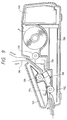
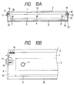
- Fig. 15 is a horizontal perspective view which illustrates an embodiment of an original document reading apparatus according to the present invention.
- Fig. 16 is a perspective view which illustrates an embodiment of the original document reading apparatus according to the present invention, Fig. 16A is an overall view and Fig. 16B is an enlarged view which illustrates a portion including the side plate.
- Referring to Figs. 15 and 16,
reference numeral 1 represents a frame, 2 represents a reading glass, 3 represents a sensor substrate, 4 represents a sensor device, 5 represents a short focal point imaging device array, 6, 7 and 8 represent lens fixing screws, 9 and 10 represent side plates, 11 and 12 represent side plate fixing screws, 13, 14 and 15 represent reading glass adhesion layers, 16 represents a bottom plate, 17 and 18 represent bottom plate fixing screws, 19 and 20 represent sensor substrate fixing rubber shafts, 21 represents an LED array, 22 represents an LED array fixing screw, 23 represents a fastening plate, 24 represents a fastening plate fixing screw, 25 represents a fastening plate side original document guide, 26 represents a lens side original document guide, 27 represents an apparatus body, 28 represents an orginal document reading apparatus fixing screw and 29 represents an original document. - The
frame 1 is formed by cutting an extruded aluminium-alloy workpiece and as well as the surface of same is subjected to a black alumite treatment in order to prevent an adverse influence upon the internal optical system and undesirable change of the state of the surface thereof. - The reading
glass 2 is chamferred on its original document introduction side so as to prevent undesirable catch of the original document. - On the
sensor substrate 3,sensor devices 4 are mounted. - The short focal point
imaging device array 5 is secured to theframe 1 by thelens fixing screws - The
side plates frame 1 by the corresponding sideplate fixing screws - The reading
glass 2 is, by the reading glass adhesion layers 13, 14 and 15, secured to the central portion, theside plates frame 1. - The
bottom plate 16 is formed by cutting an extruded aluminium-alloy workpiece and as well as the surface of same is subjected to a black alumite treatment in order to prevent undesirable change of the state of the surface thereof. Furthermore, thebottom plate 16 is secured to theframe 1 by the bottomplate fixing screws rubber shafts bottom plate 16 by adhesion or the like so that thesensor substrate 3 is fixed by the pressing force. - The
LED array 21 is constituted in such a manner that an LED chip, a cylindrical lens and the like are mounted on the substrate and the same is secured to theframe 1 by the LEDarray fixing screw 22. - The
fastening plate 23 is made of sheet metal and the same is fixed to theframe 1 by the fasteningplate fixing screw 24. The original document reading apparatus is, via thefastening plate 23, secured to theapparatus body 27 by the original document readingapparatus fixing screw 28. - According to this embodiment, the fastening plate side
original document guide 25 is formed into a guide plate to smoothly introduce the original document onto the readingglass 2, the fastening plate sideoriginal document guide 25 being secured to theapparatus body 27. - According to this embodiment, the lens side
original document guide 26 is formed into a guide plate to smoothly discharge the original document from the readingglass 2, the lens sideoriginal document guide 26 being secured to theapparatus body 27. - The
original document 29 is smoothly introduced onto the readingglass 2 along the fastening plate sideoriginal document guide 25, while the same is smoothly discharged from the readingglass 2 along the lens sideoriginal document guide 26. At this time, the surface of theoriginal document 29 confronting thereading glass 2 is illuminated on thereading glass 2 by a light beam emitted from theLED array 21. As a result, the image of theoriginal document 27 is imaged on thesensor device 4 by the short focalpoint imaging device 5. The image is then photoelectrically converted by thesensor device 4 before it is amplified on thesensor substrate 3 so as to be transmitted to outside of the original document reading apparatus. - The
frame 1 includes independent spaces, that is,hollow portions hollow portion 30 is a hollow space A claimed and defined by theframe 1, the readingglass 2, theside plates bottom plate 16. Thehollow portion 31 is a space B claimed and defined by theframe 1, theside plates hollow portions hollow portions - The
hollow portion 30 accommodates all of the optical elements such as thesensor substrate 3, the short focal pointimaging device array 5, thebottom plate 16 and theLED array 21. - On the other hand, the
hollow portion 31 does not accommodate the optical elements. Furthermore, aduct hole 40 is, as shown in Fig. 17, formed in each of theside plates hollow portion 30. Therefore, thehollow portion 31 is opened outwards at only theside plates - The
hollow portion 31 is disposed on the reverse side adjacent to theLED array 21. Since thehollow portion 31 is formed at the above-described position and air is supplied, the portion adjacent to theLED array 21, which is the heat generation source, can directly be cooled by the air supplied so that an excellent cooling effect can be obtained. - Since the reverse side portion of the
hollow portion 31 adjacent to theLED array 21 displays the highest temperature in thehollow portion 31, aradiation fin 32 formed into a rib is disposed at this position, causing an excellent cooling effect to be obtained. Since theradiation fin 32 can be manufactured simultaneously with the extrusion process, the cost can be reduced. - Furthermore, the
duct portion 33 can be provided for theframe 1 at the time of the extrusion process as shown in Fig. 18. - Although the above-described embodiment is arranged in such a manner that two independent hollow portions are formed in the original document reading apparatus, three or more hollow portions may be formed. Furthermore, a plurality of the radiation fins may be provided.
- As described above, the original document reading apparatus is arranged in such a manner that two or more independent hollow portions are formed in the frame, all of the optical elements such as the illuminating means, the imaging means and the light receiving device are accommodated in one of the independent hollow portion and the at least one side plate portion of the hollow portion except for the above-described hollow portion which accommodates the optical elements is opened to be supplied with air. Therefore, the following effects can be obtained:
- (1) Since the inside portion of the original document reading apparatus can be directly cooled, an excellent cooling efficiency can be realized.
- (2) Since the inside portion of the original document reading apparatus can be cooled by using no filter, the cost can be reduced.
- (3) Since no filter is used, the air resistance can be reduced and thereby air supply can easily be performed.
- (4) Since the hollow portion which can be supplied with air and thereby cooled can be disposed adjacent to the illuminating portion which is the heat generation portion, an excellent cooling effect can be obtained.
- (5) By providing the radiation fin, the cooling effect can further be improved.
- (6) Since the shape required to perform cooling can be formed without the secondary machining, the cost rise can be prevented.
- Fig. 19 is a modification of the above-described third embodiment in which a
fan 60 is disposed on either side surface to correspond to aduct port 40. - Cooling air sent by the
fan 60 is introduced into the hollow portion in the frame through theduct port 40 formed in theside plate 9 before it is discharged outside through theduct port 40 formed in theside plate 10. - The above-described image sensor is, similarly to the first embodiment, mounted on the image information processing apparatus shown in Fig. 9.
- Although the invention has been described in its preferred form with a certain degree of particularly, it is understood that the present disclosure of the preferred form has been charged in the details of construction and the combination and arrangement of parts may be resorted to without departing from the spirit and the scope of the invention as hereinafter claimed.
- An image sensor has a supporting member for integrally supporting a reading system including illuminating means for illuminating an original document, a photoelectrically converting means and imaging means for imaging light reflected by the surface of the original document onto the photoelectrically converting means, and has a member disposed on the side surface of the supporting member. The image sensor has two or more substantially independent spaces formed in the supporting member. The illuminating means, the imaging means and the photoelectrically converting means are accommodated in one of the spaces.
Claims (9)
- An image sensor comprising:
illuminating means for illuminating an image information surface of an original document;
imaging means for imaging light reflected from said image information surface of said original document by said illuminating means;
a light receiving device disposed on the image surface of said reflected light, arranged to photoelectrically convert said reflected light and arranged to receive image information;
a supporting member for integrally holding said illuminating means, said imaging means and said light receiving device; and
a fixing member for securing said supporting member, wherein
said supporting member is made of an electrically conductive material, an insulating film is formed on the surface of said supporting member, said fixing member includes at least electrically conductive portions and said supporting member and said fixing member are secured in such a manner that an electrical conduction is established between said supporting member and said fixing member. - An image sensor according to Claim 1, wherein means for fixing said fixing means comprises a screw at least the surface of which is electrically conductive, said supporting member is taped so that a thread hole which receives said screw is formed in said supporting member in such a manner that said film is removed and an electrical conduction is, on at least the surface of said thread hole, established between said supporting member and said fixing member when said screw is fixed.
- An image sensor according to Claim 2, wherein said supporting member is arranged in such a manner that a portion or the overall portion of its surface which comes in contact with said fixing member has no film formed thereon and an electrical conduction is, via said contact surface, established between said supporting member and said fixing member.
- An image sensor according to Claim 3, wherein said contact surface is arranged in such a manner that a mask is previously applied to the surface of said contact surface before said film is formed on the surface of said frame and said mask is removed after said film has been formed.
- An image sensor according to Claim 3, wherein said contact surface is arranged in such a manner that said film is formed on the surface of said frame and said subject portion is machined.
- An information processing apparatus on which said image sensor according to any one of Claims 1 to 5 is mounted.
- An information processing apparatus according to Claim 6 further comprising means for positioning said original document at a position at which said image sensor reads said original document.
- An information processing apparatus according to Claim 7 further comprising recording means for recording image information read by said image sensor.
- An information processing apparatus according to Claim 7, wherein said recording means is a recording head which discharges ink by utilizing thermal energy.
Applications Claiming Priority (10)
| Application Number | Priority Date | Filing Date | Title |
|---|---|---|---|
| JP324562/90 | 1990-11-26 | ||
| JP32456290 | 1990-11-26 | ||
| JP32456290 | 1990-11-26 | ||
| JP5561591 | 1991-02-28 | ||
| JP55615/91 | 1991-02-28 | ||
| JP5561591 | 1991-02-28 | ||
| JP169134/91 | 1991-06-14 | ||
| JP16913491 | 1991-06-14 | ||
| JP16913491 | 1991-06-14 | ||
| EP91120087A EP0488129B1 (en) | 1990-11-26 | 1991-11-25 | Image sensor and information processing apparatus |
Related Parent Applications (2)
| Application Number | Title | Priority Date | Filing Date |
|---|---|---|---|
| EP91120087A Division EP0488129B1 (en) | 1990-11-26 | 1991-11-25 | Image sensor and information processing apparatus |
| EP91120087.1 Division | 1991-11-25 |
Publications (3)
| Publication Number | Publication Date |
|---|---|
| EP0716535A2 true EP0716535A2 (en) | 1996-06-12 |
| EP0716535A3 EP0716535A3 (en) | 1996-06-26 |
| EP0716535B1 EP0716535B1 (en) | 2000-06-21 |
Family
ID=27295647
Family Applications (2)
| Application Number | Title | Priority Date | Filing Date |
|---|---|---|---|
| EP91120087A Expired - Lifetime EP0488129B1 (en) | 1990-11-26 | 1991-11-25 | Image sensor and information processing apparatus |
| EP96100186A Expired - Lifetime EP0716535B1 (en) | 1990-11-26 | 1991-11-25 | Image sensor and information processing apparatus |
Family Applications Before (1)
| Application Number | Title | Priority Date | Filing Date |
|---|---|---|---|
| EP91120087A Expired - Lifetime EP0488129B1 (en) | 1990-11-26 | 1991-11-25 | Image sensor and information processing apparatus |
Country Status (3)
| Country | Link |
|---|---|
| EP (2) | EP0488129B1 (en) |
| JP (1) | JP3024715B2 (en) |
| DE (2) | DE69130446T2 (en) |
Cited By (1)
| Publication number | Priority date | Publication date | Assignee | Title |
|---|---|---|---|---|
| EP1615418A1 (en) * | 2004-07-09 | 2006-01-11 | Ricoh Company, Ltd. | Image reading apparatus and image forming apparatus |
Families Citing this family (2)
| Publication number | Priority date | Publication date | Assignee | Title |
|---|---|---|---|---|
| JP3667251B2 (en) | 2000-05-30 | 2005-07-06 | キヤノン・コンポーネンツ株式会社 | Image sensor, image processing apparatus using the same, and information processing system |
| US10082768B2 (en) | 2016-12-27 | 2018-09-25 | Ricoh Company, Ltd. | Image forming apparatus |
Citations (5)
| Publication number | Priority date | Publication date | Assignee | Title |
|---|---|---|---|---|
| JPS62248365A (en) * | 1986-04-22 | 1987-10-29 | Matsushita Electric Ind Co Ltd | Photoelectric conversion device |
| JPS63182958A (en) * | 1987-01-23 | 1988-07-28 | Matsushita Electric Ind Co Ltd | Image reader |
| US4783700A (en) * | 1986-06-10 | 1988-11-08 | Canon Kabushiki Kaisha | Image sensor unit and image reading apparatus having the unit |
| EP0294834A2 (en) * | 1987-06-12 | 1988-12-14 | Canon Kabushiki Kaisha | Photo sensor and its manufacturing method and an image reading apparatus having this photo sensor |
| JPH0222872A (en) * | 1988-07-11 | 1990-01-25 | Konica Corp | Optical sensor device |
Family Cites Families (11)
| Publication number | Priority date | Publication date | Assignee | Title |
|---|---|---|---|---|
| JPS57101468A (en) * | 1980-12-17 | 1982-06-24 | Hitachi Ltd | Photo sensor array device |
| JPS60124167A (en) * | 1983-12-09 | 1985-07-03 | Canon Inc | Picture reader |
| JPS60218966A (en) * | 1984-04-16 | 1985-11-01 | Canon Inc | Adhesion reading sensor array unit |
| JPS61253588A (en) * | 1985-05-02 | 1986-11-11 | Hitachi Ltd | Optical character reader |
| JPS61278265A (en) * | 1985-06-04 | 1986-12-09 | Fuji Electric Co Ltd | Facsimile sensor unit |
| JPS62123865A (en) * | 1985-11-25 | 1987-06-05 | Toshiba Corp | Reader |
| JPS6326067A (en) * | 1986-07-18 | 1988-02-03 | Seiko Instr & Electronics Ltd | Image reading unit |
| JPS6467069A (en) * | 1987-09-07 | 1989-03-13 | Toshiba Corp | Image information reader |
| JPH01125168A (en) * | 1987-11-10 | 1989-05-17 | Matsushita Electric Ind Co Ltd | Contact type image sensor |
| JPH01216666A (en) * | 1988-02-24 | 1989-08-30 | Seiko Epson Corp | Structure of contact type image sensor |
| JPH02268563A (en) * | 1989-04-11 | 1990-11-02 | Konica Corp | Image sensor and its manufacture |
-
1991
- 1991-11-25 EP EP91120087A patent/EP0488129B1/en not_active Expired - Lifetime
- 1991-11-25 EP EP96100186A patent/EP0716535B1/en not_active Expired - Lifetime
- 1991-11-25 DE DE69130446T patent/DE69130446T2/en not_active Expired - Fee Related
- 1991-11-25 DE DE69132260T patent/DE69132260T2/en not_active Expired - Fee Related
- 1991-11-26 JP JP03335517A patent/JP3024715B2/en not_active Expired - Fee Related
Patent Citations (5)
| Publication number | Priority date | Publication date | Assignee | Title |
|---|---|---|---|---|
| JPS62248365A (en) * | 1986-04-22 | 1987-10-29 | Matsushita Electric Ind Co Ltd | Photoelectric conversion device |
| US4783700A (en) * | 1986-06-10 | 1988-11-08 | Canon Kabushiki Kaisha | Image sensor unit and image reading apparatus having the unit |
| JPS63182958A (en) * | 1987-01-23 | 1988-07-28 | Matsushita Electric Ind Co Ltd | Image reader |
| EP0294834A2 (en) * | 1987-06-12 | 1988-12-14 | Canon Kabushiki Kaisha | Photo sensor and its manufacturing method and an image reading apparatus having this photo sensor |
| JPH0222872A (en) * | 1988-07-11 | 1990-01-25 | Konica Corp | Optical sensor device |
Non-Patent Citations (3)
| Title |
|---|
| PATENT ABSTRACTS OF JAPAN vol. 12, no. 124 (E-601), 16 April 1988 & JP-A-62 248365 (MATSUSHITA ELECTRIC INDUSTRIAL CO. LTD.), 29 October 1987, * |
| PATENT ABSTRACTS OF JAPAN vol. 12, no. 457 (E-688), 30 November 1988 & JP-A-63 182958 (MATSUSHITA ELECTRIC INDUSTRIAL CO. LTD.), 28 July 1988, * |
| PATENT ABSTRACTS OF JAPAN vol. 14, no. 166 (E-911), 30 March 1990 & JP-A-02 022872 (KONICA CORP.), 25 January 1990, * |
Cited By (4)
| Publication number | Priority date | Publication date | Assignee | Title |
|---|---|---|---|---|
| EP1615418A1 (en) * | 2004-07-09 | 2006-01-11 | Ricoh Company, Ltd. | Image reading apparatus and image forming apparatus |
| US7495682B2 (en) | 2004-07-09 | 2009-02-24 | Ricoh Company, Ltd. | Image reading apparatus and image forming apparatus |
| EP2242246A3 (en) * | 2004-07-09 | 2011-02-02 | Ricoh Company, Ltd. | Image reading apparatus and image forming apparatus |
| US8194105B2 (en) | 2004-07-09 | 2012-06-05 | Ricoh Company, Ltd. | Image reading apparatus and image forming apparatus |
Also Published As
| Publication number | Publication date |
|---|---|
| EP0488129B1 (en) | 1998-11-04 |
| DE69132260T2 (en) | 2000-12-21 |
| EP0488129A2 (en) | 1992-06-03 |
| JP3024715B2 (en) | 2000-03-21 |
| EP0716535B1 (en) | 2000-06-21 |
| EP0716535A3 (en) | 1996-06-26 |
| EP0488129A3 (en) | 1993-03-17 |
| DE69130446T2 (en) | 1999-05-20 |
| DE69132260D1 (en) | 2000-07-27 |
| DE69130446D1 (en) | 1998-12-10 |
| JPH0556214A (en) | 1993-03-05 |
Similar Documents
| Publication | Publication Date | Title |
|---|---|---|
| US5281803A (en) | Image sensor and information processing apparatus | |
| US4783700A (en) | Image sensor unit and image reading apparatus having the unit | |
| US6343162B1 (en) | Contact type image sensor and information processing apparatus | |
| US5489995A (en) | Contact type image sensor, producing method of the same, and information processing apparatus | |
| JP3167111B2 (en) | Image reading device | |
| KR970011762B1 (en) | Photoelectric conversion device & information processing apparatus having the same | |
| US5581076A (en) | Contact type image sensor with more-unified construction | |
| EP0710002A2 (en) | Photoelectric conversion apparatus and information processing apparatus | |
| EP0488129B1 (en) | Image sensor and information processing apparatus | |
| EP0527223B1 (en) | Leaf-spring assembly for led printhead | |
| US4675534A (en) | Optical reader with two substrates | |
| EP0368681A2 (en) | Contact type image sensor | |
| KR100367311B1 (en) | Integral image reading/writing head, image processor provided with this, image reading head and print head | |
| JP2872488B2 (en) | Contact image sensor and method of manufacturing the same | |
| JP2731690B2 (en) | Printed circuit board assembly and electronic device having the printed circuit board assembly | |
| US5258778A (en) | Character generator for a non-mechanical printer | |
| JPH04286458A (en) | Original reader and information processing unit provided with the same | |
| DE102005041751B4 (en) | Apparatus for imaging on a recording material | |
| JP2994696B2 (en) | Contact image sensor and information processing apparatus using the sensor | |
| JP2946121B2 (en) | Contact image sensor | |
| JP2991784B2 (en) | Contact image sensor and facsimile machine using the same | |
| JPH0530283A (en) | Original picture reader | |
| JP4458593B2 (en) | Light amount detection member and image reading apparatus having the same | |
| JPH0461549A (en) | Close contact image sensor and information processor using the sensor | |
| JPH04239258A (en) | Picture reader and recording system using the picture reader |
Legal Events
| Date | Code | Title | Description |
|---|---|---|---|
| PUAI | Public reference made under article 153(3) epc to a published international application that has entered the european phase |
Free format text: ORIGINAL CODE: 0009012 |
|
| PUAL | Search report despatched |
Free format text: ORIGINAL CODE: 0009013 |
|
| AC | Divisional application: reference to earlier application |
Ref document number: 488129 Country of ref document: EP |
|
| AK | Designated contracting states |
Kind code of ref document: A2 Designated state(s): DE FR GB |
|
| AK | Designated contracting states |
Kind code of ref document: A3 Designated state(s): DE FR GB |
|
| 17P | Request for examination filed |
Effective date: 19961112 |
|
| 17Q | First examination report despatched |
Effective date: 19980727 |
|
| GRAG | Despatch of communication of intention to grant |
Free format text: ORIGINAL CODE: EPIDOS AGRA |
|
| GRAG | Despatch of communication of intention to grant |
Free format text: ORIGINAL CODE: EPIDOS AGRA |
|
| GRAH | Despatch of communication of intention to grant a patent |
Free format text: ORIGINAL CODE: EPIDOS IGRA |
|
| GRAH | Despatch of communication of intention to grant a patent |
Free format text: ORIGINAL CODE: EPIDOS IGRA |
|
| GRAA | (expected) grant |
Free format text: ORIGINAL CODE: 0009210 |
|
| AC | Divisional application: reference to earlier application |
Ref document number: 488129 Country of ref document: EP |
|
| AK | Designated contracting states |
Kind code of ref document: B1 Designated state(s): DE FR GB |
|
| REF | Corresponds to: |
Ref document number: 69132260 Country of ref document: DE Date of ref document: 20000727 |
|
| ET | Fr: translation filed | ||
| PLBE | No opposition filed within time limit |
Free format text: ORIGINAL CODE: 0009261 |
|
| STAA | Information on the status of an ep patent application or granted ep patent |
Free format text: STATUS: NO OPPOSITION FILED WITHIN TIME LIMIT |
|
| 26N | No opposition filed | ||
| REG | Reference to a national code |
Ref country code: GB Ref legal event code: IF02 |
|
| PGFP | Annual fee paid to national office [announced via postgrant information from national office to epo] |
Ref country code: DE Payment date: 20071122 Year of fee payment: 17 |
|
| PGFP | Annual fee paid to national office [announced via postgrant information from national office to epo] |
Ref country code: GB Payment date: 20071121 Year of fee payment: 17 Ref country code: FR Payment date: 20071108 Year of fee payment: 17 |
|
| GBPC | Gb: european patent ceased through non-payment of renewal fee |
Effective date: 20081125 |
|
| REG | Reference to a national code |
Ref country code: FR Ref legal event code: ST Effective date: 20090731 |
|
| PG25 | Lapsed in a contracting state [announced via postgrant information from national office to epo] |
Ref country code: DE Free format text: LAPSE BECAUSE OF NON-PAYMENT OF DUE FEES Effective date: 20090603 |
|
| PG25 | Lapsed in a contracting state [announced via postgrant information from national office to epo] |
Ref country code: GB Free format text: LAPSE BECAUSE OF NON-PAYMENT OF DUE FEES Effective date: 20081125 |
|
| PG25 | Lapsed in a contracting state [announced via postgrant information from national office to epo] |
Ref country code: FR Free format text: LAPSE BECAUSE OF NON-PAYMENT OF DUE FEES Effective date: 20081130 |