EP0716519A1 - Procédé et dispositif pour l'échange de données entre une unité de transmission et une mémoire tampon ainsi que récupération d'horloge - Google Patents
Procédé et dispositif pour l'échange de données entre une unité de transmission et une mémoire tampon ainsi que récupération d'horloge Download PDFInfo
- Publication number
- EP0716519A1 EP0716519A1 EP95116784A EP95116784A EP0716519A1 EP 0716519 A1 EP0716519 A1 EP 0716519A1 EP 95116784 A EP95116784 A EP 95116784A EP 95116784 A EP95116784 A EP 95116784A EP 0716519 A1 EP0716519 A1 EP 0716519A1
- Authority
- EP
- European Patent Office
- Prior art keywords
- clock
- dpll
- oscillator
- data stream
- locked loop
- Prior art date
- Legal status (The legal status is an assumption and is not a legal conclusion. Google has not performed a legal analysis and makes no representation as to the accuracy of the status listed.)
- Withdrawn
Links
Images

Classifications
-
- H—ELECTRICITY
- H04—ELECTRIC COMMUNICATION TECHNIQUE
- H04J—MULTIPLEX COMMUNICATION
- H04J3/00—Time-division multiplex systems
- H04J3/02—Details
- H04J3/06—Synchronising arrangements
- H04J3/062—Synchronisation of signals having the same nominal but fluctuating bit rates, e.g. using buffers
- H04J3/0626—Synchronisation of signals having the same nominal but fluctuating bit rates, e.g. using buffers plesiochronous multiplexing systems, e.g. plesiochronous digital hierarchy [PDH], jitter attenuators
-
- G—PHYSICS
- G06—COMPUTING; CALCULATING OR COUNTING
- G06F—ELECTRIC DIGITAL DATA PROCESSING
- G06F2205/00—Indexing scheme relating to group G06F5/00; Methods or arrangements for data conversion without changing the order or content of the data handled
- G06F2205/06—Indexing scheme relating to groups G06F5/06 - G06F5/16
- G06F2205/061—Adapt frequency, i.e. clock frequency at one side is adapted to clock frequency, or average clock frequency, at the other side; Not pulse stuffing only
Definitions
- the present invention relates to a method according to the preamble of patent claim 1 and a circuit arrangement according to the preamble of patent claim 5.
- the combination of different digital telecommunications networks not only requires identical signaling for proper operation between participants in the telecommunications networks involved, but also requires that the clock frequencies in the telecommunications networks essentially match and also have a predetermined stability. For this reason, transmission units are provided at the interface between the two telecommunications networks which have a high jitter tolerance on the input side, so that an incoming data stream with a strongly fluctuating clock rate can be received without errors in the transmission unit. On the transmission side of these transmission units, on the other hand, an outgoing data stream that is as jitter-free as possible is sought in order to be able to guarantee the highest possible transmission security when the data is distributed.
- a known transmission unit is described in European patent application EP-0 572 367 A1, in which a transmission unit is specified in which a clock signal is available on the transmission side, which corresponds to the clock rate of the incoming data stream including any jitter, and which is used directly for reading in the Data is used in a buffer memory contained in the transmission unit.
- a phase locked loop PLL - Phase Locked Loop
- PLL Phase Locked Loop
- the clock rate of the incoming data stream must be reconstructed using a clock regeneration circuit (DE-32 34 576 A1). This can be carried out, for example, with a digital phase locked loop, which means that the transmission unit must also have a second oscillator in addition to a second phase locked loop. It is precisely these additional circuits that place increased demands and, in particular, cause additional costs for an overall integration of the circuit of a transmission unit.
- the present invention is therefore based on the object of specifying a transmission unit which can be implemented more simply and significantly more cost-effectively.
- the invention has the following advantages: since the clock rate of the transmission unit on the output side is used as a reference frequency for the clock regeneration circuit on the input side, there is no oscillator compared to the known transmission unit, which leads to considerable savings in the implementation of a circuit for the transmission unit and thus to further cost reductions.
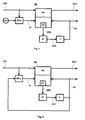
- Fig. 1 shows a known transmission unit with a clock regeneration circuit DPLL, a fixed value oscillator OSZ, a controlled oscillator V, a loop filter LP and a switching unit SE, which consists essentially of a buffer memory PS and a phase discriminator PD.
- the switching unit SE or the buffer memory PS is acted upon on the input side by an incoming data stream DAI which is simultaneously fed to the clock regeneration circuit DPLL.
- the clock regeneration circuit DPLL is supplied with a reference frequency generated in the fixed value oscillator OSZ, which is used together with the transmission rate of the incoming data stream DAI to generate a write clock FI, with which the data of the incoming data stream DAI are written into the buffer memory PS.
- the clock regeneration circuit DPLL is preferably implemented as a digital phase locked loop.
- a possible embodiment can be found in German Offenlegungsschrift DE 32 34 576 A1.
- An outgoing data stream DAO and a reading clock FO are provided on the output side of the transmission unit, which corresponds to the data transmission rate of the outgoing data stream DAO and which is supplied to the switching unit SE for reading the data from the buffer memory PS.
- the reading clock FO is generated in a further phase locked loop, which consists of the loop filter LP, the controlled oscillator V and the phase discriminator PD contained in the switching unit SE. Further information on this phase-locked loop can be found, for example, in documents EP-0 572 367 A1 and EP-0 204 894 B1.
- the phase-locked loop of the clock regeneration circuit DPLL is of low quality (U. Tietze and Ch. Schenk, "Semiconductor Circuitry", Springer Verlag, 6th edition, page 22), with which the write clock FI with the has the same jitter as the coming data stream DAI.
- the data of the coming data stream DAI are thus read without errors into the buffer memory PS of the switching unit SE.
- the data read with the reading clock FO from the buffer memory PS are available in the outgoing data stream DAO together with the reading clock FO.
- the reading clock FO is jitter-free in accordance with the quality selected for this phase locked loop.
- the clock regeneration circuit DPLL preferably consists of a digital phase locked loop, which, however, requires an external reference frequency.
- the known transmission unit has a total of two phase locked loops and two oscillators, which causes considerable costs and a corresponding space requirement in the circuit implementation of the transmission unit.
- FIG. 2 shows the transmission unit according to the invention, which differs from the known transmission unit shown in FIG. 1 in that the reading clock FO of the oscillator V is used as the reference frequency for the clock regeneration circuit DPLL.
- the fixed value oscillator OSZ used in the known teaching according to the explanations for FIG. 1 is no longer necessary, which leads to corresponding cost savings due to the smaller amount of circuitry required for the entire transmission unit, because a smaller circuit area is required for an overall integration of the circuit of the transmission unit.
- phase-locked loop of the clock regeneration circuit DPLL By returning the reading clock FO to the clock-side regeneration circuit DPLL on the input side, two control systems are interleaved, which can be unstable if their parameters are chosen unfavorably.
- time constant U. Tietze and Ch. Schenk, "semiconductor circuit technology", Springer publishers, 6th edition, pages 11 and 15
- the transmission unit is stable.
- the phase-locked loop on the output side is therefore of a higher quality than the phase-locked loop of the clock regeneration circuit DPLL.
- the reading clock FO for forming the outgoing data stream DAO is fixed to a predetermined frequency value that comes directly from the oscillator V, which is a fixed value oscillator in this embodiment.
- this transmission unit is rigid with respect to the transmission frequency, since the oscillator V is not regulated. In this embodiment of the transmission unit, therefore, neither a phase discriminator PD (FIG. 2) in the switching unit SE nor a loop filter LP (FIG. 2) is necessary.
- the circuit arrangement shown in FIG. 3 can be used in a known PDH (Plesiochronous Digital Hierarchy) multiplexer, in which the incoming data are packaged in a frame-structured outgoing data stream.
- the transmission rate of the outgoing data stream is therefore slightly higher than that of the incoming data stream. Bits that become free are filled with so-called "empty" stuff bits.
Landscapes
- Engineering & Computer Science (AREA)
- Computer Hardware Design (AREA)
- Computer Networks & Wireless Communication (AREA)
- Signal Processing (AREA)
- Synchronisation In Digital Transmission Systems (AREA)
Applications Claiming Priority (2)
| Application Number | Priority Date | Filing Date | Title |
|---|---|---|---|
| CH3677/94 | 1994-12-05 | ||
| CH03677/94A CH690152A5 (de) | 1994-12-05 | 1994-12-05 | Verfahren zur Datenübertragung über eine Uebertragungseinheit und eine Schaltungsanordnung zur Durchführung des Verfahrens. |
Publications (1)
| Publication Number | Publication Date |
|---|---|
| EP0716519A1 true EP0716519A1 (fr) | 1996-06-12 |
Family
ID=4261142
Family Applications (1)
| Application Number | Title | Priority Date | Filing Date |
|---|---|---|---|
| EP95116784A Withdrawn EP0716519A1 (fr) | 1994-12-05 | 1995-10-25 | Procédé et dispositif pour l'échange de données entre une unité de transmission et une mémoire tampon ainsi que récupération d'horloge |
Country Status (3)
| Country | Link |
|---|---|
| EP (1) | EP0716519A1 (fr) |
| CH (1) | CH690152A5 (fr) |
| NO (1) | NO954918L (fr) |
Cited By (4)
| Publication number | Priority date | Publication date | Assignee | Title |
|---|---|---|---|---|
| WO1998044671A1 (fr) * | 1997-04-02 | 1998-10-08 | Qualcomm Incorporated | Procede et systeme de transmission synchronisee de donnees a un reseau ayant un signal d'horloge de reference |
| WO2002051060A2 (fr) * | 2000-12-20 | 2002-06-27 | Primarion, Inc. | Synchronisation de donnees de boucle a phase asservie et de boucle a asservissement retard pll/(dll) utilisant un indicateur de niveau de remplissage granulaire fifo |
| WO2002058317A2 (fr) * | 2000-12-20 | 2002-07-25 | Primarion, Inc. | Synchronisation de donnees a l'aide d'une boucle double pll/dll |
| EP1542382A1 (fr) * | 2003-12-08 | 2005-06-15 | Alcatel | Procédé et circuit d'entrée pour transférer un flux des données d'entrée en rafale |
Citations (3)
| Publication number | Priority date | Publication date | Assignee | Title |
|---|---|---|---|---|
| EP0067971A2 (fr) * | 1981-06-23 | 1982-12-29 | ANT Nachrichtentechnik GmbH | Dispositif de réduction de variations de phase dans une horloge de sortie de mémoires élastiques |
| EP0435383A2 (fr) * | 1989-12-23 | 1991-07-03 | Philips Patentverwaltung GmbH | Circuit d'adaptation de débit binaire |
| JPH04246939A (ja) * | 1991-02-01 | 1992-09-02 | Nec Corp | スタッフジッタ抑圧回路 |
-
1994
- 1994-12-05 CH CH03677/94A patent/CH690152A5/de not_active IP Right Cessation
-
1995
- 1995-10-25 EP EP95116784A patent/EP0716519A1/fr not_active Withdrawn
- 1995-12-04 NO NO954918A patent/NO954918L/no not_active Application Discontinuation
Patent Citations (3)
| Publication number | Priority date | Publication date | Assignee | Title |
|---|---|---|---|---|
| EP0067971A2 (fr) * | 1981-06-23 | 1982-12-29 | ANT Nachrichtentechnik GmbH | Dispositif de réduction de variations de phase dans une horloge de sortie de mémoires élastiques |
| EP0435383A2 (fr) * | 1989-12-23 | 1991-07-03 | Philips Patentverwaltung GmbH | Circuit d'adaptation de débit binaire |
| JPH04246939A (ja) * | 1991-02-01 | 1992-09-02 | Nec Corp | スタッフジッタ抑圧回路 |
Non-Patent Citations (1)
| Title |
|---|
| PATENT ABSTRACTS OF JAPAN vol. 17, no. 19 (E - 1306) 13 January 1993 (1993-01-13) * |
Cited By (8)
| Publication number | Priority date | Publication date | Assignee | Title |
|---|---|---|---|---|
| WO1998044671A1 (fr) * | 1997-04-02 | 1998-10-08 | Qualcomm Incorporated | Procede et systeme de transmission synchronisee de donnees a un reseau ayant un signal d'horloge de reference |
| WO2002051060A2 (fr) * | 2000-12-20 | 2002-06-27 | Primarion, Inc. | Synchronisation de donnees de boucle a phase asservie et de boucle a asservissement retard pll/(dll) utilisant un indicateur de niveau de remplissage granulaire fifo |
| WO2002058317A2 (fr) * | 2000-12-20 | 2002-07-25 | Primarion, Inc. | Synchronisation de donnees a l'aide d'une boucle double pll/dll |
| WO2002051060A3 (fr) * | 2000-12-20 | 2003-01-23 | Primarion Inc | Synchronisation de donnees de boucle a phase asservie et de boucle a asservissement retard pll/(dll) utilisant un indicateur de niveau de remplissage granulaire fifo |
| WO2002058317A3 (fr) * | 2000-12-20 | 2003-12-31 | Primarion Inc | Synchronisation de donnees a l'aide d'une boucle double pll/dll |
| US7366270B2 (en) | 2000-12-20 | 2008-04-29 | Primarion, Inc. | PLL/DLL dual loop data synchronization utilizing a granular FIFO fill level indicator |
| US7743168B2 (en) | 2000-12-20 | 2010-06-22 | Primarion Corporation | PLL/DLL dual loop data synchronization |
| EP1542382A1 (fr) * | 2003-12-08 | 2005-06-15 | Alcatel | Procédé et circuit d'entrée pour transférer un flux des données d'entrée en rafale |
Also Published As
| Publication number | Publication date |
|---|---|
| NO954918L (no) | 1996-06-06 |
| CH690152A5 (de) | 2000-05-15 |
| NO954918D0 (no) | 1995-12-04 |
Similar Documents
| Publication | Publication Date | Title |
|---|---|---|
| DE3107232C2 (fr) | ||
| DE60029826T2 (de) | Mehrratentransportsystem sowie chipsatz | |
| DE69432587T2 (de) | Verzögerungsleitungsseparator für datenbus | |
| DE3886819T2 (de) | Digitaler Asynchron-Synchronmultiplexer/Demultiplexer mit asynchroner Taktregeneration. | |
| EP0429888B1 (fr) | Méthode de transmission par un réseau multiplex hierarchisé synchrone et numérique d'un signal à large bande distribué entre des unités de transmission subordonnées | |
| DE69232057T2 (de) | Digitale schaltungen zur taktentflatterung mit minimalem zittern | |
| DE69217526T2 (de) | Linearer In-line-Desynchronisierer | |
| EP0507385A2 (fr) | Système de transmission pour la hiérarchie numérique synchrone | |
| EP0475498B1 (fr) | Circuit d'adaption du débit binaire de deux signaux numériques | |
| EP0503732A2 (fr) | Système de transmission pour la hiérarchie numérique synchrone | |
| DE10014477A1 (de) | Verfahren und System zum Synchronisieren von mehreren Untersystemen unter Anwendung eines spannungsgesteuerten Oszillators | |
| EP0708541A1 (fr) | Système de transmission avec une boucle de commande | |
| DE69411511T2 (de) | Schaltung zur Taktrückgewinnung mit angepassten Oszillatoren | |
| DE4336239A1 (de) | Schaltungsanordnung für einen Taktgenerator | |
| DE69229668T2 (de) | Synchrone Schaltung | |
| EP0777351B1 (fr) | Système de transmission numérique synchrone | |
| DE2757462A1 (de) | Elastischer speicher zur unterdrueckung einer phasenstoerung in einem system zur uebertragung von digitalsignalen | |
| DE69128835T2 (de) | Logische Maschine zur Verarbeitung von Kontrollinformation eines Telekommunikation-Übertragungsrahmens | |
| DE2616380B2 (de) | Schaltungsanordnung zur Synchronisierung eines Emgabetaktes mit einem Ausgabetakt bei einem Pufferspeicher für digitale Daten | |
| EP0716519A1 (fr) | Procédé et dispositif pour l'échange de données entre une unité de transmission et une mémoire tampon ainsi que récupération d'horloge | |
| EP0963069A2 (fr) | Système de désynchronisation pour système de transmission digitale synchrone | |
| EP0456903B1 (fr) | Procédé et dispositif de réduction de jitter à temps d'attente | |
| EP1094610A1 (fr) | Boucle de verrouillage de phase numérique | |
| DE69221748T2 (de) | Schaltungsanordnung zur Taktrückgewinnung | |
| DE10260713A1 (de) | Digital steuerbarer Oszillator |
Legal Events
| Date | Code | Title | Description |
|---|---|---|---|
| PUAI | Public reference made under article 153(3) epc to a published international application that has entered the european phase |
Free format text: ORIGINAL CODE: 0009012 |
|
| 17P | Request for examination filed |
Effective date: 19951121 |
|
| AK | Designated contracting states |
Kind code of ref document: A1 Designated state(s): AT CH DE ES GB IT LI |
|
| STAA | Information on the status of an ep patent application or granted ep patent |
Free format text: STATUS: THE APPLICATION IS DEEMED TO BE WITHDRAWN |
|
| 18D | Application deemed to be withdrawn |
Effective date: 20010508 |