EP0712017A2 - Optoelectronic component - Google Patents
Optoelectronic component Download PDFInfo
- Publication number
- EP0712017A2 EP0712017A2 EP95116668A EP95116668A EP0712017A2 EP 0712017 A2 EP0712017 A2 EP 0712017A2 EP 95116668 A EP95116668 A EP 95116668A EP 95116668 A EP95116668 A EP 95116668A EP 0712017 A2 EP0712017 A2 EP 0712017A2
- Authority
- EP
- European Patent Office
- Prior art keywords
- spherical body
- semiconductor element
- led
- housing
- opening edge
- Prior art date
- Legal status (The legal status is an assumption and is not a legal conclusion. Google has not performed a legal analysis and makes no representation as to the accuracy of the status listed.)
- Withdrawn
Links
Images

Classifications
-
- G—PHYSICS
- G02—OPTICS
- G02B—OPTICAL ELEMENTS, SYSTEMS OR APPARATUS
- G02B6/00—Light guides; Structural details of arrangements comprising light guides and other optical elements, e.g. couplings
- G02B6/24—Coupling light guides
- G02B6/42—Coupling light guides with opto-electronic elements
- G02B6/4201—Packages, e.g. shape, construction, internal or external details
- G02B6/4219—Mechanical fixtures for holding or positioning the elements relative to each other in the couplings; Alignment methods for the elements, e.g. measuring or observing methods especially used therefor
- G02B6/4236—Fixing or mounting methods of the aligned elements
- G02B6/4237—Welding
Definitions
- the invention relates to an optoelectronic component according to the precharacterising part of claim 1.
- the invention also relates to a method for mounting of such an optoelectronic component.
- An optoelectronic component of the kind mentioned in the introductory part of claim 1 is known, for example from EP-B-O 583 331.
- the optoelectronic component may, for example, be intended to be connected to a light guide.
- the optoelectronic element may, for example, be a light-emitting diode (LED) which emits light in the light guide, or a photodetector which detects light from the light guide.
- LED light-emitting diode
- the housing comprises a body with a cylindrical recess.
- the LED is surrounded by a mounting body in the form of a ring with a double-curved envelope surface.
- the envelope surface has a spherical shape with a diameter which coincides with the diameter of the recess.
- the intensity of the light emitted from the far end of the light guide is measured.
- By rotating and axially displacing the LED with the mounting ring in the recess it can be adjusted so as to obtain a maximum value of the intensity.
- the LED is mechanically locked to the housing with the aid of a fast-curing resin, whereafter the gap between the ring and the recess is filled with a resin with a high mechanical stability, for example epoxy resin.
- the LED When the LED, provided with a mounting ring, is to be welded to the recess, the problem arises as to where to place a welded joint. To make it possible to weld, the distance between two points to be welded must not exceed a certain maximally tolerable distance. Since the LED with the mounting ring is inserted a certain distance into the recess, the distance from the opening edge of the recess to that point where the distance between the mounting ring and the recess is lower than the maximally tolerable distance becomes too large to make access to welding possible (see Figure 5 in the above-mentioned publication). The adjustment of the LED along its symmetry axis also causes problems since the position of the welded joint will vary between different components.
- the invention aims at providing an optoelectronic component of the above-mentioned kind which enables the connection between the housing and the semiconductor element to be made by welding without endangering adjustment to maximum luminous efficiency of the optoelectronic component.
- the invention suggests an optoelectronic component according to the introductory part of claim 1, which is characterized by the features of the characterizing part of claim 1.
- a method for mounting an optoelectronic component according to the invention is characterized by the features of claim 6.
- the invention solves the problem as to how to join an optoelectronic semiconductor element provided with a mounting ring to the housing. It provides a completely tight joint between the optoelectronic semiconductor element, the mounting ring and the housing.
- the mounting method according to the invention offers a fast, simple and efficient adjustment of the optoelectronic semiconductor element included in the component.
- the method comprises adjustment of the optoelectronic semiconductor element in the axial direction, to a recess in the housing so as to obtain said completely tight joint.
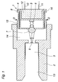
- Figure 1 shows an optoelectronic component which constitutes one embodiment of the invention.
- the component comprises an optoelectronic semiconductor element which in this case is an LED 1.
- the LED is arranged in a housing 2, which is provided with means for connection of a light guide 3.
- the LED is adapted to emit radiation towards the light guide for transmission therethrough.
- the LED 1 has a base 4, on which is mounted a semiconductor body 5 which constitutes the active and light-emitting element of the LED. Adjacent to the semiconductor body there is arranged a lens 6 for focussing the radiation. Further, the LED has a cover 8 which is provided with an exit opening for the radiation, in which a lens 7 is arranged. The lenses 6 and 7 focus the radiation towards the optical fibre end 9 of the light guide 3.
- the LED is provided with schematically shown connection conductors 10, 11, and its base is filled with glass or a plastic material 12. In that end of the LED which faces away from the light guide, the base 4 and the cover 8 together form an outwardly directed flange, hereinafter referred to as light-emitting flange 16, which runs around the whole LED.
- the housing 2 is made of metal and is substantially rotationally symmetrical.
- the housing is provided with an axial bore 13 for accommodating the light guide 3.
- the housing In the righthand part of the housing 2, as shown in the figure, the housing has a cylindrical recess 14.
- the symmetry axis of the housing and the optical axis of the LED coincide approximately with the longitudinal axis of the light guide 3, hereinafter referred to as the z axis.
- the LED 1 is surrounded by a mounting body in the form of a mounting ring 15 of a weldable metal, for example stainless steel.
- Figure 2 shows the mounting ring 15 which is rotationally symmetrical with a symmetry axis E-E.
- the mounting ring has a round hole 20 for receiving the LED 1.
- the lefthand part of the mounting ring as shown in the figure, has an external envelope surface 21 with an approximately spherical shape and with a centre at the point 22, and a diameter d which substantially corresponds to the diameter D of the cylindrical recess 14.
- the mounting ring has its largest periphery 25 where its outer circumference is equal to the diameter d of the spherically formed envelope surface.
- the righthand part 23 of the mounting ring has the shape of a straight cylinder and is provided with an outwardly directed flange furthest to the right, hereinafter referred to as a mounting flange 24, which runs around the whole mounting ring.
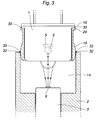
- FIG. 3 shows that end of the housing 2 in which the LED is arranged and is intended to illustrate the method for mounting.
- the LED 1 is first joined to the mounting ring 15 by welding the mounting flange 24 and the LED flange 16 to each other around the whole LED such that a hermetically sealed joint 30 is obtained.
- the LED, mounted in the mounting ring is inserted into the recess 14 in the housing.
- the LED is inserted so far that that part of the mounting ring which has the largest periphery 25, that is, that part of the mounting ring which has an outer circumference corresponding to the circumference of the recess, is on a level with the opening edge 32 of the recess.
- the LED is connected to a current source and is caused to emit light. Light beams emitted from the LED are focussed towards a point at the end of the light guide. In general, this point will not be located at the end surface of the optical fibre 9, the reason for this being unavoidable deviations during manufacturing and mounting.
- a measuring member is connected to the opposite end of the light guide 3 for detection of the intensity of the light which exits from the light guide.
- the LED in the mounting ring can now be rotated and also be axially displaced until maximum intensity is obtained in the light detected at the opposite end of the light guide.
- the LED is then in its position of maximum intensity and is fixed in relation to the housing by means of at least three weld points between the opening edge and the mounting ring, whereupon the current source is disconnected. Thereafter, the opening edge and the mounting ring are welded to each other by means of a welded joint 33 running around the whole opening edge, thus obtaining a hermetically sealed joint.
- An advantageous welding method to use in the invention is laser welding.
- the distance between two points to be welded to each other may not exceed 50 ⁇ m.
- the gap opening which is formed between the opening edge and the mounting ring not exceed 50 ⁇ m.
- This gap opening will hereinafter be referred to as the welding gap. Measurements have shown that the LED maximally needs to be adjusted about 0.2 mm in each direction in the axial direction. For mounting reasons, the recess and the mounting ring cannot have exactly the same diameter, but the mounting ring must have a diameter which is somewhat smaller than the diameter of the recess.
- a welding gap is formed which is at most 10 ⁇ m.
- the method is not suited for welding of semiconductor elements with too small dimensions.
- the size of the welding gap that may be bridged is, of course, dependent on which welding method is applied.
- an optoelectronic component with hermetically sealed joints is obtained with a fast and simple mounting and an efficient adjustment.
- the LED in the above example may, of course, consist of another optoelectronic semiconductor element, for example a laser diode or a photodetector.
- the component described above is intended for connection to a light guide.
- the invention is not limited to this case but may be applied and provide the same advantages also in connection with other fields of use.
Abstract
Description
- The invention relates to an optoelectronic component according to the precharacterising part of
claim 1. The invention also relates to a method for mounting of such an optoelectronic component. - An optoelectronic component of the kind mentioned in the introductory part of
claim 1 is known, for example from EP-B-O 583 331. The optoelectronic component may, for example, be intended to be connected to a light guide. The optoelectronic element may, for example, be a light-emitting diode (LED) which emits light in the light guide, or a photodetector which detects light from the light guide. - From the above-mentioned publication it is known to arrange an LED such that it is adjustable in relation to the light guide when mounting the optoelectronic component. The symmetry axis of the optoelectronic component and the optical axis of the LED coincide approximately with the longitudinal axis of the light guide. The housing comprises a body with a cylindrical recess. The LED is surrounded by a mounting body in the form of a ring with a double-curved envelope surface. The envelope surface has a spherical shape with a diameter which coincides with the diameter of the recess. When mounting the component, the light guide is first mounted in the housing, whereupon the LED with a mounting ring is pushed a certain distance into the recess and is connected to a current source. The intensity of the light emitted from the far end of the light guide is measured. By rotating and axially displacing the LED with the mounting ring in the recess, it can be adjusted so as to obtain a maximum value of the intensity. In this position, the LED is mechanically locked to the housing with the aid of a fast-curing resin, whereafter the gap between the ring and the recess is filled with a resin with a high mechanical stability, for example epoxy resin.
- One disadvantage of using resin for joining together the LED and the housing is that there is a certain risk of the joint leaking moisture or other gases. Another disadvantage is that the resin must cure for a certain time before the component endures being moved, which entails an extension of the mounting time. It is, therefore, desirable for the LED and the housing instead to be joined together by means of a welded joint. The advantages of a welded joint are that it is completely tight, has a high mechanical strength, and needs no time for curing.
- When the LED, provided with a mounting ring, is to be welded to the recess, the problem arises as to where to place a welded joint. To make it possible to weld, the distance between two points to be welded must not exceed a certain maximally tolerable distance. Since the LED with the mounting ring is inserted a certain distance into the recess, the distance from the opening edge of the recess to that point where the distance between the mounting ring and the recess is lower than the maximally tolerable distance becomes too large to make access to welding possible (see Figure 5 in the above-mentioned publication). The adjustment of the LED along its symmetry axis also causes problems since the position of the welded joint will vary between different components.
- To avoid the above-mentioned problems, attempts were made to mount the LED direct in the recess without the mounting ring. This led to the creation of a space between the LED and the recess, which made possible adjustment of the LED in directions perpendicular to its symmetry axis. That end of the LED which faces away from the light guide has a flange which runs around the whole LED. After the adjustment, the opening edge of the recess and the flange of the LED were welded to each other. This method of mounting does not provide for any axial displacement of the LED and hence no adjustment of the LED in relation to the light guide in the axial direction. It was found that this gave such a poor adjustment of the LED that a majority of the mounted components had to be rejected. The conclusion is that an adjustment of the LED in the axial direction is necessary to obtain an acceptable luminous efficiency between the LED and the light guide.
- The invention aims at providing an optoelectronic component of the above-mentioned kind which enables the connection between the housing and the semiconductor element to be made by welding without endangering adjustment to maximum luminous efficiency of the optoelectronic component.
- To achieve this aim the invention suggests an optoelectronic component according to the introductory part of
claim 1, which is characterized by the features of the characterizing part ofclaim 1. - Further developments of the optoelectronic component are characterized by the features of the
additional claims 2 to 5. - A method for mounting an optoelectronic component according to the invention is characterized by the features of
claim 6. - Further developments of this method are characterized by the features of the
additional claims - The invention solves the problem as to how to join an optoelectronic semiconductor element provided with a mounting ring to the housing. It provides a completely tight joint between the optoelectronic semiconductor element, the mounting ring and the housing.
- The mounting method according to the invention offers a fast, simple and efficient adjustment of the optoelectronic semiconductor element included in the component. The method comprises adjustment of the optoelectronic semiconductor element in the axial direction, to a recess in the housing so as to obtain said completely tight joint.
- By way of example, the invention will now be described in greater detail with reference to the accompanying drawings showing in
- Figure 1
- a section through a component according to the invention, which comprises an LED and connection means for a light guide,
- Figure 2
- a section through a mounting body for adjustable mounting of the LED,
- Figure 3 ,
- with reference to a section through the component, the principle of adjustment and attachment of the LED.
- Figure 1 shows an optoelectronic component which constitutes one embodiment of the invention. The component comprises an optoelectronic semiconductor element which in this case is an
LED 1. The LED is arranged in ahousing 2, which is provided with means for connection of alight guide 3. The LED is adapted to emit radiation towards the light guide for transmission therethrough. - The
LED 1 has abase 4, on which is mounted asemiconductor body 5 which constitutes the active and light-emitting element of the LED. Adjacent to the semiconductor body there is arranged alens 6 for focussing the radiation. Further, the LED has acover 8 which is provided with an exit opening for the radiation, in which alens 7 is arranged. Thelenses optical fibre end 9 of thelight guide 3. The LED is provided with schematically shownconnection conductors 10, 11, and its base is filled with glass or aplastic material 12. In that end of the LED which faces away from the light guide, thebase 4 and thecover 8 together form an outwardly directed flange, hereinafter referred to as light-emittingflange 16, which runs around the whole LED. - The
housing 2 is made of metal and is substantially rotationally symmetrical. The housing is provided with anaxial bore 13 for accommodating thelight guide 3. In the righthand part of thehousing 2, as shown in the figure, the housing has acylindrical recess 14. The symmetry axis of the housing and the optical axis of the LED coincide approximately with the longitudinal axis of thelight guide 3, hereinafter referred to as the z axis. - The
LED 1 is surrounded by a mounting body in the form of amounting ring 15 of a weldable metal, for example stainless steel. Figure 2 shows the mountingring 15 which is rotationally symmetrical with a symmetry axis E-E. The mounting ring has around hole 20 for receiving theLED 1. The lefthand part of the mounting ring, as shown in the figure, has anexternal envelope surface 21 with an approximately spherical shape and with a centre at thepoint 22, and a diameter d which substantially corresponds to the diameter D of thecylindrical recess 14. The mounting ring has itslargest periphery 25 where its outer circumference is equal to the diameter d of the spherically formed envelope surface. Therighthand part 23 of the mounting ring, as shown in the figure, has the shape of a straight cylinder and is provided with an outwardly directed flange furthest to the right, hereinafter referred to as a mountingflange 24, which runs around the whole mounting ring. - Figure 3 shows that end of the
housing 2 in which the LED is arranged and is intended to illustrate the method for mounting. During mounting, theLED 1 is first joined to the mountingring 15 by welding the mountingflange 24 and theLED flange 16 to each other around the whole LED such that a hermetically sealed joint 30 is obtained. Thereafter, the LED, mounted in the mounting ring, is inserted into therecess 14 in the housing. The LED is inserted so far that that part of the mounting ring which has thelargest periphery 25, that is, that part of the mounting ring which has an outer circumference corresponding to the circumference of the recess, is on a level with the openingedge 32 of the recess. - The LED is connected to a current source and is caused to emit light. Light beams emitted from the LED are focussed towards a point at the end of the light guide. In general, this point will not be located at the end surface of the
optical fibre 9, the reason for this being unavoidable deviations during manufacturing and mounting. A measuring member is connected to the opposite end of thelight guide 3 for detection of the intensity of the light which exits from the light guide. The LED in the mounting ring can now be rotated and also be axially displaced until maximum intensity is obtained in the light detected at the opposite end of the light guide. The LED is then in its position of maximum intensity and is fixed in relation to the housing by means of at least three weld points between the opening edge and the mounting ring, whereupon the current source is disconnected. Thereafter, the opening edge and the mounting ring are welded to each other by means of a welded joint 33 running around the whole opening edge, thus obtaining a hermetically sealed joint. - An advantageous welding method to use in the invention is laser welding. During laser welding, the distance between two points to be welded to each other may not exceed 50 µm. Thus, it is a condition for a successful welding that the gap opening which is formed between the opening edge and the mounting ring not exceed 50 µm. This gap opening will hereinafter be referred to as the welding gap. Measurements have shown that the LED maximally needs to be adjusted about 0.2 mm in each direction in the axial direction. For mounting reasons, the recess and the mounting ring cannot have exactly the same diameter, but the mounting ring must have a diameter which is somewhat smaller than the diameter of the recess. When the mounting ring before being adjusted is placed in the recess with its largest periphery on a level with the opening edge, a welding gap is formed which is at most 10 µm. In this example, the recess, and hence also the spherical part of the mounting ring, have a diameter d = D = 5 mm. A movement of 0.2 mm in the axial direction of the mounting ring from the position at the beginning of the adjustment gives an increase of the welding gap of about 8 µm, that is, the welding gap becomes about 18 µm. Since it is not certain that the LED is centred in the recess, the welding gap may maximally be 2-18 µm = 36 µm, which is considerably less than 50 µm.
- The calculation of the increase of the opening gap is performed as follows:
x + z = r (the equation for a sphere) wherein
r = the radius of the sphere = 2.5 mm
x = r - s
s = the gap width
z = the movement in the axial direction = 0.2 mm
- If r = 1.5 mm ⇒ s = 14 µm ⇒ the maximum welding gap becomes 2-14 µm + 20 µm = 48 µm.
- As will be clear from the above reasoning, the method is not suited for welding of semiconductor elements with too small dimensions. The size of the welding gap that may be bridged is, of course, dependent on which welding method is applied.
- During a mounting method according to the invention, an optoelectronic component with hermetically sealed joints is obtained with a fast and simple mounting and an efficient adjustment.
- The LED in the above example may, of course, consist of another optoelectronic semiconductor element, for example a laser diode or a photodetector.
- The component described above is intended for connection to a light guide. However, the invention is not limited to this case but may be applied and provide the same advantages also in connection with other fields of use.
Claims (8)
- An optoelectronic component comprising a housing (2) and an optoelectronic semiconductor element (1) mounted in a spherical body (15) which is adjustably journalled in a cylindrical recess (14) in the housing (2), the diameter of the spherical body and the diameter of the cylindrical recess being substantially the same, characterized in that the cylindrical recess (14) has an opening edge (32) which is joined to the spherical body (15) by means of a welded joint (33) running around the whole opening edge so as to obtain a hermetically sealed joint.
- An optoelectronic component according to claim 1, characterized in that the spherical body (15) is annular and surrounds the optoelectronic semiconductor element (1).
- An optoelectronic component according to claim 1 or 2, characterized in that the optoelectronic semiconductor element (1) and the spherical body (15) are joined together by a welded joint (30).
- An optoelectronic component according to claim 3, characterized in that the optoelectronic semiconductor element (1) and the spherical body (15) are joined together by a welded joint (30) running around the whole semiconductor element, thus forming a hermetically sealed joint.
- An optoelectronic component according to any or the preceding claims, characterized in that the housing (2) comprises means for connection of a light guide (3) for transmission of light from (or to) the optoelectronic semiconductor element (1).
- A method for mounting an optoelectronic component comprising a housing (2) and an optoelectronic semiconductor element (1) mounted in a spherical body (15) which is adjustably journalled in a cylindrical recess (14) in the housing, the diameter of the spherical body and the diameter of the cylindrical recess being substantially the same, characterized in that- the optoelectronic semiconductor element (1) is arranged in the spherical body (15) and is welded thereto,- the spherical body and the semiconductor element arranged therein are arranged in the recess (14) with its largest periphery (25) at the opening edge (32) of the recess,- the orientation and position of the semiconductor element are adjusted, and- the spherical body (15) and the housing (2) are welded to each other by a welded joint (33) arranged at the opening edge.
- A method according to claim 6, characterized in that the opening edge (32) and the spherical body (15) are joined together by means of a welded joint running around the whole opening edge, thus obtaining a hermetically sealed joint.
- A method according to claim 6 or 7, characterized in that the opening edge (32) and the spherical body (15) are first fixed to each other by a number of weld points and thereafter joined together by means of a welded joint running around the whole opening edge.
Applications Claiming Priority (2)
| Application Number | Priority Date | Filing Date | Title |
|---|---|---|---|
| SE9403648 | 1994-10-25 | ||
| SE9403648A SE503416C2 (en) | 1994-10-25 | 1994-10-25 | Optoelectric component and method of mounting such |
Publications (2)
| Publication Number | Publication Date |
|---|---|
| EP0712017A2 true EP0712017A2 (en) | 1996-05-15 |
| EP0712017A3 EP0712017A3 (en) | 1996-06-05 |
Family
ID=20395734
Family Applications (1)
| Application Number | Title | Priority Date | Filing Date |
|---|---|---|---|
| EP95116668A Withdrawn EP0712017A2 (en) | 1994-10-25 | 1995-10-23 | Optoelectronic component |
Country Status (4)
| Country | Link |
|---|---|
| US (1) | US5604361A (en) |
| EP (1) | EP0712017A2 (en) |
| JP (1) | JPH08211257A (en) |
| SE (1) | SE503416C2 (en) |
Cited By (1)
| Publication number | Priority date | Publication date | Assignee | Title |
|---|---|---|---|---|
| WO2007065457A1 (en) * | 2005-12-07 | 2007-06-14 | Pirelli & C. S.P.A. | Optical assembly connecting a laser with an optical fibre |
Families Citing this family (27)
| Publication number | Priority date | Publication date | Assignee | Title |
|---|---|---|---|---|
| JPH09307144A (en) * | 1996-05-14 | 1997-11-28 | Matsushita Electric Ind Co Ltd | Light emitting element and its manufacture |
| US5896214A (en) * | 1996-07-01 | 1999-04-20 | Intermec Ip Corp. | Mounting bracket for mounting electronic components in a portable electronic device and method of making same |
| US5831290A (en) * | 1997-02-25 | 1998-11-03 | Quarton, Inc. | Laser diode mounting structure |
| US6092935A (en) * | 1997-08-22 | 2000-07-25 | Siemens Aktiengesellschaft | Optoelectronic transmitting and/or receiving module and method for its production |
| JP3196699B2 (en) * | 1997-09-04 | 2001-08-06 | 住友電気工業株式会社 | Optical component assembling method and optical component |
| DE10053670A1 (en) * | 2000-10-28 | 2002-05-08 | Daimler Chrysler Ag | Optical signal transmission system |
| US20030095755A1 (en) * | 2001-11-16 | 2003-05-22 | Vladimir Vaganov | Feature and method to align and assemble photonic components |
| US6905259B2 (en) * | 2001-12-31 | 2005-06-14 | Texas Instruments Incorporated | Tilt-in-place alignment system and method |
| US6826336B2 (en) * | 2002-05-22 | 2004-11-30 | The Boeing Company | Fiber optic LED illuminator |
| US7072534B2 (en) * | 2002-07-22 | 2006-07-04 | Applied Materials, Inc. | Optical ready substrates |
| US7110629B2 (en) * | 2002-07-22 | 2006-09-19 | Applied Materials, Inc. | Optical ready substrates |
| US7043106B2 (en) * | 2002-07-22 | 2006-05-09 | Applied Materials, Inc. | Optical ready wafers |
| US7044648B1 (en) * | 2003-01-10 | 2006-05-16 | Avanex Corporation | Method and apparatus for a fiber optic housing and aligning device |
| KR20060026027A (en) * | 2003-05-29 | 2006-03-22 | 어플라이드 머티어리얼스, 인코포레이티드 | Serial routing of optical signals |
| EP1649566A4 (en) * | 2003-06-27 | 2007-08-15 | Applied Materials Inc | Pulsed quantum dot laser system with low jitter |
| US20050016446A1 (en) | 2003-07-23 | 2005-01-27 | Abbott John S. | CaF2 lenses with reduced birefringence |
| US20060222024A1 (en) * | 2005-03-15 | 2006-10-05 | Gray Allen L | Mode-locked semiconductor lasers with quantum-confined active region |
| US20060227825A1 (en) * | 2005-04-07 | 2006-10-12 | Nl-Nanosemiconductor Gmbh | Mode-locked quantum dot laser with controllable gain properties by multiple stacking |
| FR2887996B1 (en) * | 2005-06-30 | 2007-08-17 | Prismaflex Internat Sa | RETROECTION COMMUNICATION PANEL |
| WO2007027615A1 (en) | 2005-09-01 | 2007-03-08 | Applied Materials, Inc. | Ridge technique for fabricating an optical detector and an optical waveguide |
| US7561607B2 (en) * | 2005-12-07 | 2009-07-14 | Innolume Gmbh | Laser source with broadband spectrum emission |
| WO2007065614A2 (en) * | 2005-12-07 | 2007-06-14 | Innolume Gmbh | Laser source with broadband spectrum emission |
| US7835408B2 (en) * | 2005-12-07 | 2010-11-16 | Innolume Gmbh | Optical transmission system |
| EP1884809B1 (en) * | 2006-07-31 | 2018-02-14 | TE Connectivity Corporation | Expanded beam connector |
| WO2010065731A2 (en) * | 2008-12-03 | 2010-06-10 | Innolume Gmbh | Semiconductor laser with low relative intensity noise of individual longitudinal modes and optical transmission system incorporating the laser |
| US8731347B2 (en) * | 2012-10-11 | 2014-05-20 | Avago Technologies General Ip (Singapore) Pte. Ltd. | Lens standoff and protection for optical communication systems |
| CN103605192B (en) * | 2013-11-29 | 2015-07-15 | 武汉光迅科技股份有限公司 | Optical coupling device and manufacturing method thereof |
Citations (1)
| Publication number | Priority date | Publication date | Assignee | Title |
|---|---|---|---|---|
| EP0583331B1 (en) | 1991-05-06 | 1998-03-04 | Asea Brown Boveri Ab | Optoelectronic component |
Family Cites Families (1)
| Publication number | Priority date | Publication date | Assignee | Title |
|---|---|---|---|---|
| GB9112087D0 (en) * | 1991-06-05 | 1991-07-24 | Gca Electronics Ltd | Fibre optic device and its manufacture |
-
1994
- 1994-10-25 SE SE9403648A patent/SE503416C2/en not_active IP Right Cessation
-
1995
- 1995-10-23 EP EP95116668A patent/EP0712017A2/en not_active Withdrawn
- 1995-10-24 US US08/547,321 patent/US5604361A/en not_active Expired - Fee Related
- 1995-10-24 JP JP7275940A patent/JPH08211257A/en active Pending
Patent Citations (1)
| Publication number | Priority date | Publication date | Assignee | Title |
|---|---|---|---|---|
| EP0583331B1 (en) | 1991-05-06 | 1998-03-04 | Asea Brown Boveri Ab | Optoelectronic component |
Cited By (2)
| Publication number | Priority date | Publication date | Assignee | Title |
|---|---|---|---|---|
| WO2007065457A1 (en) * | 2005-12-07 | 2007-06-14 | Pirelli & C. S.P.A. | Optical assembly connecting a laser with an optical fibre |
| US7909518B2 (en) | 2005-12-07 | 2011-03-22 | Pgt Photonics S.P.A. | Optical assembly connecting a laser with optical fibre |
Also Published As
| Publication number | Publication date |
|---|---|
| US5604361A (en) | 1997-02-18 |
| SE9403648L (en) | 1996-04-26 |
| SE9403648D0 (en) | 1994-10-25 |
| SE503416C2 (en) | 1996-06-10 |
| EP0712017A3 (en) | 1996-06-05 |
| JPH08211257A (en) | 1996-08-20 |
Similar Documents
| Publication | Publication Date | Title |
|---|---|---|
| EP0712017A2 (en) | Optoelectronic component | |
| US5386488A (en) | Optical module and manufacturing method therefor | |
| US4988159A (en) | Fiber tailed optoelectronic transducer | |
| EP0363496B1 (en) | Semiconductor laser module and positioning method thereof | |
| JP2875812B2 (en) | Optoelectronic device with coupling between optical fiber and semiconductor laser diode | |
| US6865333B2 (en) | Visual alignment of multiple-reflector collimation system | |
| EP0441403B1 (en) | Method of fabricating an optical package | |
| US6935791B2 (en) | Apparatus and methods for micro-positioning and alignment | |
| US20210033804A1 (en) | Transistor outline package and method for producing a transistor outline package | |
| US6742938B2 (en) | Optical module for coupling an optical semiconductor element having a sealing cap with an optical fiber | |
| USH551H (en) | Optical package with improved fiber alignment fixture | |
| WO2002068998A2 (en) | Fiber-optic cable alignment system | |
| CN107764294B (en) | Fusion welding packaging device for optical fiber Fabry-Perot sensor | |
| JPS6120911A (en) | Coupling device between light emitting element and optical fiber | |
| JPH01181488A (en) | Semiconductor laser device | |
| JPH0196610A (en) | Optical coupling device | |
| JP2713941B2 (en) | Optoelectronic device with optical coupler and method of manufacturing the same | |
| JPS63241505A (en) | Semiconductor laser diode package | |
| JPH0964482A (en) | Laser beam generation device | |
| JPH0894889A (en) | Semiconductor laser module | |
| US6705770B2 (en) | Method of manufacturing a receptacled opto-electronic module | |
| JPS61255312A (en) | Coupling device for optical element | |
| KR100402828B1 (en) | The optical coupling apparatus and method of photo diode housing | |
| JPS63223723A (en) | Structure for fixing photosemiconductor collimator | |
| JP2003279795A (en) | Optical fiber collimator and manufacturing method thereof |
Legal Events
| Date | Code | Title | Description |
|---|---|---|---|
| PUAI | Public reference made under article 153(3) epc to a published international application that has entered the european phase |
Free format text: ORIGINAL CODE: 0009012 |
|
| PUAL | Search report despatched |
Free format text: ORIGINAL CODE: 0009013 |
|
| AK | Designated contracting states |
Kind code of ref document: A2 Designated state(s): DE ES FR GB IT |
|
| AK | Designated contracting states |
Kind code of ref document: A3 Designated state(s): DE ES FR GB IT |
|
| 17P | Request for examination filed |
Effective date: 19960617 |
|
| 17Q | First examination report despatched |
Effective date: 20010615 |
|
| STAA | Information on the status of an ep patent application or granted ep patent |
Free format text: STATUS: THE APPLICATION IS DEEMED TO BE WITHDRAWN |
|
| 18D | Application deemed to be withdrawn |
Effective date: 20040501 |