EP0710985A1 - X-ray image sensor - Google Patents
X-ray image sensor Download PDFInfo
- Publication number
- EP0710985A1 EP0710985A1 EP95116643A EP95116643A EP0710985A1 EP 0710985 A1 EP0710985 A1 EP 0710985A1 EP 95116643 A EP95116643 A EP 95116643A EP 95116643 A EP95116643 A EP 95116643A EP 0710985 A1 EP0710985 A1 EP 0710985A1
- Authority
- EP
- European Patent Office
- Prior art keywords
- image
- scintillator
- image sensor
- converters
- ray image
- Prior art date
- Legal status (The legal status is an assumption and is not a legal conclusion. Google has not performed a legal analysis and makes no representation as to the accuracy of the status listed.)
- Granted
Links
- 239000000835 fiber Substances 0.000 claims description 21
- 230000008878 coupling Effects 0.000 claims 1
- 238000010168 coupling process Methods 0.000 claims 1
- 238000005859 coupling reaction Methods 0.000 claims 1
- 230000003287 optical effect Effects 0.000 abstract 3
- 239000013307 optical fiber Substances 0.000 abstract 2
- 238000010276 construction Methods 0.000 description 1
- 238000009607 mammography Methods 0.000 description 1
- 239000011159 matrix material Substances 0.000 description 1
- 230000005855 radiation Effects 0.000 description 1
Images

Classifications
-
- H—ELECTRICITY
- H01—ELECTRIC ELEMENTS
- H01L—SEMICONDUCTOR DEVICES NOT COVERED BY CLASS H10
- H01L25/00—Assemblies consisting of a plurality of individual semiconductor or other solid state devices ; Multistep manufacturing processes thereof
- H01L25/03—Assemblies consisting of a plurality of individual semiconductor or other solid state devices ; Multistep manufacturing processes thereof all the devices being of a type provided for in the same subgroup of groups H01L27/00 - H01L33/00, or in a single subclass of H10K, H10N, e.g. assemblies of rectifier diodes
- H01L25/04—Assemblies consisting of a plurality of individual semiconductor or other solid state devices ; Multistep manufacturing processes thereof all the devices being of a type provided for in the same subgroup of groups H01L27/00 - H01L33/00, or in a single subclass of H10K, H10N, e.g. assemblies of rectifier diodes the devices not having separate containers
- H01L25/065—Assemblies consisting of a plurality of individual semiconductor or other solid state devices ; Multistep manufacturing processes thereof all the devices being of a type provided for in the same subgroup of groups H01L27/00 - H01L33/00, or in a single subclass of H10K, H10N, e.g. assemblies of rectifier diodes the devices not having separate containers the devices being of a type provided for in group H01L27/00
- H01L25/0655—Assemblies consisting of a plurality of individual semiconductor or other solid state devices ; Multistep manufacturing processes thereof all the devices being of a type provided for in the same subgroup of groups H01L27/00 - H01L33/00, or in a single subclass of H10K, H10N, e.g. assemblies of rectifier diodes the devices not having separate containers the devices being of a type provided for in group H01L27/00 the devices being arranged next to each other
-
- H—ELECTRICITY
- H01—ELECTRIC ELEMENTS
- H01L—SEMICONDUCTOR DEVICES NOT COVERED BY CLASS H10
- H01L2924/00—Indexing scheme for arrangements or methods for connecting or disconnecting semiconductor or solid-state bodies as covered by H01L24/00
- H01L2924/0001—Technical content checked by a classifier
- H01L2924/0002—Not covered by any one of groups H01L24/00, H01L24/00 and H01L2224/00
Definitions
- X-ray images can be produced by an X-ray image sensor that has a flat electronic image converter (e.g. a CCD) that is preceded by a scintillator as a fluorescent screen.
- the image converter is optically coupled to the scintillator and generates image signals from which an image of the examined area of a patient can be generated electronically.
- the image converters that can be implemented today have limited dimensions, so that large objects can only be detected by complex design, in particular by the fiber optics that conduct the light from the scintillator to the image converter.
- the invention has for its object to design an X-ray image sensor based on electronic image converters so that a relatively large image area is created with a simple construction.
- the optically inactive edge zones in which e.g. Gate connections and registers are located, do not cause gaps in the X-ray image.
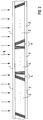
- FIG. 1 shows a scintillator 1 which is optically coupled to image converters 3 with the aid of fiber optics 2.
- the drawing shows that a plurality of image converters 3 adjoin one another in one area. They have optically inactive edge zones 4.
- the fiber optics 2 are under one so that no image dropouts are caused thereby from 90 ° different angles to the image converter 3 and the scintillator 1 inclined. They adjoin each other on the scintillator 1, thus capture the entire image of the scintillator 1, but leave the edge zones 4 of the image converter 3 free.
- the fiber optics 2 consist of bundles of parallel fibers which are cut off at the end at an angle deviating from 90 ° to the fiber axis. They are placed between the> image converter 3 and the scintillator 1 in such a way that they adjoin one another on the scintillator 1, but leave the edge zones 4 free.
- Arrows 6 also show the X-ray radiation that strikes the scintillator 1.
- the fiber optics 2 also serve to shield the image converter 3 against the X-rays.
- the image converter 3 covers a relatively large image field, so that relatively large objects can also be recorded. They can be in a row, but also as a matrix of e.g. four image converters can be arranged.
- Fig. 2 shows an embodiment in which the left fiber optic 2 in Fig. 1 is replaced by a fiber optic 5 which is perpendicular to the image converter 3, i.e. in contrast to the fiber optics 2 at an angle of 90 ° to the image converter 3.
- the edge zones 4 of the image converter 3 are also left free in this solution.
- FIG. 3 shows a solution in which three fiber optics 2, 5, 2 follow one another, corresponding to the sequence of three image converters 3.
- An X-ray image sensor of the type described is particularly suitable for mammography.
Abstract
Description
Röntgenbilder können durch einen Röntgenbildsensor angefertigt werden, der einen flächenhaften elektronischen Bildwandler (z.B. ein CCD) aufweist, dem ein Szintillator als Leuchtschirm vorgeschaltet ist. Der Bildwandler wird dabei optisch am Szintillator angekoppelt und erzeugt Bildsignale, aus denen ein Bild des untersuchten Bereiches eines Patienten elektronisch generiert werden kann. Die heute realisierbaren Bildwandler haben jedoch limitierte Abmessungen, so daß große Objekte dadurch nur durch aufwendige konstruktive Gestaltung, insbesondere der das Licht vom Szintillator auf den Bildwandler leitenden Fiberoptik erfaßt werden können.X-ray images can be produced by an X-ray image sensor that has a flat electronic image converter (e.g. a CCD) that is preceded by a scintillator as a fluorescent screen. The image converter is optically coupled to the scintillator and generates image signals from which an image of the examined area of a patient can be generated electronically. However, the image converters that can be implemented today have limited dimensions, so that large objects can only be detected by complex design, in particular by the fiber optics that conduct the light from the scintillator to the image converter.
Der Erfindung liegt die Aufgabe zugrunde, einen Röntgenbildsensor auf der Basis von elektronischen Bildwandlern so zu gestalten, daß bei einfachem konstruktivem Aufbau eine relativ große Bildfläche geschaffen wird.The invention has for its object to design an X-ray image sensor based on electronic image converters so that a relatively large image area is created with a simple construction.
Diese Aufgabe ist erfindungsgemäß gelost durch die Merkmale des Patentanspruches. Bei dem erfindungsgemäßen Röntgenbildsensor grenzen z.B. mehrere CCD-Bildwandler aneinander, wobei die optisch nicht aktiven Randzonen, in denen z.B. Gate-Anschlüsse und Register liegen, keine Lücken im Röntgenbild verursachen.According to the invention, this object is achieved by the features of the patent claim. In the X-ray image sensor according to the invention, e.g. several CCD image converters together, the optically inactive edge zones, in which e.g. Gate connections and registers are located, do not cause gaps in the X-ray image.
Die Erfindung ist nachfolgend anhand von drei in den Fig. 1 bis 3 dargestellten Ausführungsbeispielen näher erläutert.The invention is explained in more detail below with reference to three exemplary embodiments shown in FIGS. 1 to 3.
In der Fig. 1 ist ein Szintillator 1 dargestellt, der mit Hilfe von Fiberoptiken 2 an Bildwandlern 3 optisch angekoppelt ist. Die Zeichnung zeigt, daß mehrere Bildwandler 3 in einer Fläche aneinander angrenzen. Sie weisen optisch nicht aktive Randzonen 4 auf. Damit dadurch keine Bildausfälle verursacht werden, sind die Fiberoptiken 2 unter einem von 90° abweichenden Winkel gegenüber den Bildwandlern 3 und dem Szintillator 1 geneigt. Sie grenzen dabei am Szintillator 1 aneinander an, erfassen also das gesamte Bild des Szintillators 1, lassen jedoch die Randzonen 4 der Bildwandler 3 frei.1 shows a scintillator 1 which is optically coupled to
Die Fiberoptiken 2 bestehen aus Bündeln paralleler Fasern, die unter einem von 90° abweichenden Winkel zur Faserachse stirnseitig abgeschnitten sind. Sie sind so zwischen die >Bildwandler 3 und den Szintillator 1 gelegt, daß sie am Szintillator 1 aneinander angrenzen, die Randzonen 4 jedoch freilassen.The
Durch Pfeile 6 ist noch die Röntgenstrahlung dargestellt, die auf dem Szintillator 1 auftrifft. Die Fiberoptiken 2 dienen auch zur Abschirmung der Bildwandler 3 gegen die Röntgenstrahlung. Die Bildwandler 3 decken ein relativ großes Bildfeld ab, so daß auch relativ große Objekte aufgenommen werden können. Sie können in einer Reihe, aber auch als Matrix von z.B. vier Bildwandlern angeordnet sein.
Die Fig. 2 zeigt eine Ausführungsform, bei der die linke Fiberoptik 2 in Fig. 1 durch eine Fiberoptik 5 ersetzt ist, welche senkrecht zu den Bildwandlern 3 verläuft, d.h. im Gegensatz zur Fiberoptik 2 unter einem Winkel von 90° zu dem Bildwandler 3 liegt. Auch bei dieser Lösung sind die Randzonen 4 der Bildwandler 3 freigelassen.Fig. 2 shows an embodiment in which the left fiber optic 2 in Fig. 1 is replaced by a fiber optic 5 which is perpendicular to the
Schließlich zeigt die Fig. 3 eine Lösung, bei der drei Fiberoptiken 2, 5, 2 aufeinanderfolgen, entsprechend der Aufeinanderfolge von drei Bildwandlern 3.Finally, FIG. 3 shows a solution in which three
Ein Röntgenbildsensor der beschriebenen Art eignet sich besonders für die Mammographie.An X-ray image sensor of the type described is particularly suitable for mammography.
Claims (4)
Applications Claiming Priority (4)
| Application Number | Priority Date | Filing Date | Title |
|---|---|---|---|
| DE4439260 | 1994-11-03 | ||
| DE4439260 | 1994-11-03 | ||
| DE19503034A DE19503034A1 (en) | 1994-11-03 | 1995-01-31 | X-ray image sensor |
| DE19503034 | 1995-01-31 |
Publications (2)
| Publication Number | Publication Date |
|---|---|
| EP0710985A1 true EP0710985A1 (en) | 1996-05-08 |
| EP0710985B1 EP0710985B1 (en) | 1998-03-25 |
Family
ID=25941653
Family Applications (1)
| Application Number | Title | Priority Date | Filing Date |
|---|---|---|---|
| EP95116643A Expired - Lifetime EP0710985B1 (en) | 1994-11-03 | 1995-10-23 | X-ray image sensor |
Country Status (3)
| Country | Link |
|---|---|
| US (1) | US5563414A (en) |
| EP (1) | EP0710985B1 (en) |
| JP (1) | JPH08211155A (en) |
Families Citing this family (13)
| Publication number | Priority date | Publication date | Assignee | Title |
|---|---|---|---|---|
| US5715292A (en) * | 1994-11-25 | 1998-02-03 | Loral Fairchild Corporation | Digital sensor cassette for mammography |
| US6005911A (en) | 1995-11-17 | 1999-12-21 | Trex Medical Corporation | Large area array, single exposure digital mammography |
| EP1148349A4 (en) | 1998-12-14 | 2003-07-09 | Hamamatsu Photonics Kk | Optical element and radiation detector using the same |
| JP3276614B2 (en) * | 1999-04-22 | 2002-04-22 | 浜松ホトニクス株式会社 | Optical element, radiation image sensor, and method of manufacturing optical element |
| JP3595759B2 (en) | 1999-07-02 | 2004-12-02 | キヤノン株式会社 | Imaging apparatus and imaging system |
| US6800857B2 (en) * | 2000-08-10 | 2004-10-05 | Canon Kabushiki Kaisha | Large-area fiber plate, radiation image pickup apparatus utilizing the same and producing method therefor |
| US6800870B2 (en) * | 2000-12-20 | 2004-10-05 | Michel Sayag | Light stimulating and collecting methods and apparatus for storage-phosphor image plates |
| SE0100382D0 (en) * | 2001-02-07 | 2001-02-07 | Lp Roentgenteknik Ab | X-ray detector |
| JP3870156B2 (en) * | 2002-02-07 | 2007-01-17 | キヤノン株式会社 | Fiber plate and manufacturing method thereof, radiation imaging apparatus, and radiation imaging system |
| IL158345A0 (en) * | 2003-10-09 | 2004-05-12 | Interon As | Pixel detector and method of manufacture and assembly thereof |
| JP7046698B2 (en) * | 2018-04-24 | 2022-04-04 | 浜松ホトニクス株式会社 | Radiation detector, manufacturing method of radiation detector, and image processing method |
| JP7206431B2 (en) * | 2018-04-24 | 2023-01-17 | 浜松ホトニクス株式会社 | Radiation detector, radiation detector manufacturing method, and image processing method |
| CN109545810A (en) * | 2018-11-20 | 2019-03-29 | 京东方科技集团股份有限公司 | A kind of flat panel detector and preparation method thereof |
Citations (4)
| Publication number | Priority date | Publication date | Assignee | Title |
|---|---|---|---|---|
| EP0296737A1 (en) * | 1987-06-15 | 1988-12-28 | Seiko Instruments Inc. | X-ray radiation sensor |
| WO1991015785A1 (en) * | 1990-04-11 | 1991-10-17 | Washington University | Method and apparatus for forming plastic multi-fiber |
| US5138642A (en) * | 1989-03-02 | 1992-08-11 | Innovative Imaging Systems, Inc. | Detector imaging arrangement for an industrial CT device |
| EP0597725A1 (en) * | 1992-11-13 | 1994-05-18 | Debex (Proprietary) Limited | System for scanning bodies |
Family Cites Families (6)
| Publication number | Priority date | Publication date | Assignee | Title |
|---|---|---|---|---|
| US4179100A (en) * | 1977-08-01 | 1979-12-18 | University Of Pittsburgh | Radiography apparatus |
| JPS58210582A (en) * | 1982-05-31 | 1983-12-07 | Shimadzu Corp | Radiation position detector |
| US4755681A (en) * | 1986-09-30 | 1988-07-05 | Shimadzu Corporation | Radiation image detecting apparatus with IC modules stacked stepwise |
| JPH0344966A (en) * | 1989-07-13 | 1991-02-26 | Sony Corp | Solid-state image pickup device |
| JP2507282Y2 (en) * | 1990-11-26 | 1996-08-14 | 株式会社モリタ製作所 | Medical X-ray image detector |
| US5391879A (en) * | 1993-11-19 | 1995-02-21 | Minnesota Mining And Manufacturing Company | Radiation detector |
-
1995
- 1995-10-13 US US08/542,910 patent/US5563414A/en not_active Expired - Lifetime
- 1995-10-23 EP EP95116643A patent/EP0710985B1/en not_active Expired - Lifetime
- 1995-10-31 JP JP7283284A patent/JPH08211155A/en active Pending
Patent Citations (4)
| Publication number | Priority date | Publication date | Assignee | Title |
|---|---|---|---|---|
| EP0296737A1 (en) * | 1987-06-15 | 1988-12-28 | Seiko Instruments Inc. | X-ray radiation sensor |
| US5138642A (en) * | 1989-03-02 | 1992-08-11 | Innovative Imaging Systems, Inc. | Detector imaging arrangement for an industrial CT device |
| WO1991015785A1 (en) * | 1990-04-11 | 1991-10-17 | Washington University | Method and apparatus for forming plastic multi-fiber |
| EP0597725A1 (en) * | 1992-11-13 | 1994-05-18 | Debex (Proprietary) Limited | System for scanning bodies |
Also Published As
| Publication number | Publication date |
|---|---|
| EP0710985B1 (en) | 1998-03-25 |
| JPH08211155A (en) | 1996-08-20 |
| US5563414A (en) | 1996-10-08 |
Similar Documents
| Publication | Publication Date | Title |
|---|---|---|
| EP0710985A1 (en) | X-ray image sensor | |
| DE10160723A1 (en) | CT detector module with improved scintillator / diode coupling | |
| DE3118458C2 (en) | Light receiving device | |
| DE19610816C2 (en) | Backlight system for a scoreboard | |
| DE3609669C2 (en) | ||
| DE3111746C2 (en) | Photoelectric converter | |
| EP0064736A1 (en) | Light pick-up device | |
| DE19753268A1 (en) | Collimator for computer tomography system with X-ray source and detection array | |
| DE2529073C2 (en) | Coupling element for fiber optic light guides | |
| EP1014684A2 (en) | Apparatus and method for reading on a phosphorlayer stored data | |
| EP0381786A1 (en) | Optical data transmission device | |
| DE2811435A1 (en) | ROENTGEN DETECTOR | |
| DE102009038028A1 (en) | Detector arrangement with increased sensitivity | |
| DE102008063323A1 (en) | Radiation detector, light detector assembly, manufacturing method and imaging system | |
| DE60025191T2 (en) | METHOD AND DEVICE FOR SIMPLIFIED ALIGNMENT IN X-RAY IMAGING | |
| DE3616530A1 (en) | ARRANGEMENT OF OPTICAL ELEMENTS | |
| DE19503034A1 (en) | X-ray image sensor | |
| EP2240801A2 (en) | Device and method for recording an image | |
| WO2003079372A1 (en) | Detector for x-ray computer tomography scanners | |
| EP3217408A2 (en) | Focussing module for a form filter and form filter for adjusting a spatial intensity distribution of a x-ray beam | |
| EP1124251A3 (en) | Electron energy filter with magnetic deflection unit | |
| DE2729291C2 (en) | Photoelectric imager | |
| DE1805097C3 (en) | Arrangement for generating coordinate signals corresponding to the displacements of a freely movable stylus in a writing plane | |
| DE2655227A1 (en) | LIGHT TRANSFER DEVICE | |
| DE3742920C2 (en) |
Legal Events
| Date | Code | Title | Description |
|---|---|---|---|
| PUAI | Public reference made under article 153(3) epc to a published international application that has entered the european phase |
Free format text: ORIGINAL CODE: 0009012 |
|
| AK | Designated contracting states |
Kind code of ref document: A1 Designated state(s): DE FR GB IT |
|
| 17P | Request for examination filed |
Effective date: 19960604 |
|
| 17Q | First examination report despatched |
Effective date: 19970515 |
|
| GRAG | Despatch of communication of intention to grant |
Free format text: ORIGINAL CODE: EPIDOS AGRA |
|
| GRAG | Despatch of communication of intention to grant |
Free format text: ORIGINAL CODE: EPIDOS AGRA |
|
| GRAH | Despatch of communication of intention to grant a patent |
Free format text: ORIGINAL CODE: EPIDOS IGRA |
|
| GRAH | Despatch of communication of intention to grant a patent |
Free format text: ORIGINAL CODE: EPIDOS IGRA |
|
| GRAA | (expected) grant |
Free format text: ORIGINAL CODE: 0009210 |
|
| AK | Designated contracting states |
Kind code of ref document: B1 Designated state(s): DE FR GB IT |
|
| REF | Corresponds to: |
Ref document number: 59501697 Country of ref document: DE Date of ref document: 19980430 |
|
| ET | Fr: translation filed | ||
| GBT | Gb: translation of ep patent filed (gb section 77(6)(a)/1977) |
Effective date: 19980507 |
|
| ITF | It: translation for a ep patent filed |
Owner name: STUDIO JAUMANN P. & C. S.N.C. |
|
| PGFP | Annual fee paid to national office [announced via postgrant information from national office to epo] |
Ref country code: FR Payment date: 19981023 Year of fee payment: 4 |
|
| PLBE | No opposition filed within time limit |
Free format text: ORIGINAL CODE: 0009261 |
|
| STAA | Information on the status of an ep patent application or granted ep patent |
Free format text: STATUS: NO OPPOSITION FILED WITHIN TIME LIMIT |
|
| 26N | No opposition filed | ||
| PG25 | Lapsed in a contracting state [announced via postgrant information from national office to epo] |
Ref country code: GB Free format text: LAPSE BECAUSE OF NON-PAYMENT OF DUE FEES Effective date: 19991023 |
|
| GBPC | Gb: european patent ceased through non-payment of renewal fee |
Effective date: 19991023 |
|
| PG25 | Lapsed in a contracting state [announced via postgrant information from national office to epo] |
Ref country code: FR Free format text: LAPSE BECAUSE OF NON-PAYMENT OF DUE FEES Effective date: 20000630 |
|
| REG | Reference to a national code |
Ref country code: FR Ref legal event code: ST |
|
| PGFP | Annual fee paid to national office [announced via postgrant information from national office to epo] |
Ref country code: DE Payment date: 20041220 Year of fee payment: 10 |
|
| PG25 | Lapsed in a contracting state [announced via postgrant information from national office to epo] |
Ref country code: IT Free format text: LAPSE BECAUSE OF NON-PAYMENT OF DUE FEES;WARNING: LAPSES OF ITALIAN PATENTS WITH EFFECTIVE DATE BEFORE 2007 MAY HAVE OCCURRED AT ANY TIME BEFORE 2007. THE CORRECT EFFECTIVE DATE MAY BE DIFFERENT FROM THE ONE RECORDED. Effective date: 20051023 |
|
| PG25 | Lapsed in a contracting state [announced via postgrant information from national office to epo] |
Ref country code: DE Free format text: LAPSE BECAUSE OF NON-PAYMENT OF DUE FEES Effective date: 20060503 |