EP0704793B1 - Method and circuit to compare the sum of two numbers to a third number - Google Patents
Method and circuit to compare the sum of two numbers to a third number Download PDFInfo
- Publication number
- EP0704793B1 EP0704793B1 EP95306861A EP95306861A EP0704793B1 EP 0704793 B1 EP0704793 B1 EP 0704793B1 EP 95306861 A EP95306861 A EP 95306861A EP 95306861 A EP95306861 A EP 95306861A EP 0704793 B1 EP0704793 B1 EP 0704793B1
- Authority
- EP
- European Patent Office
- Prior art keywords
- cinr
- value
- xor
- values
- sum
- Prior art date
- Legal status (The legal status is an assumption and is not a legal conclusion. Google has not performed a legal analysis and makes no representation as to the accuracy of the status listed.)
- Expired - Lifetime
Links
Images

Classifications
-
- G—PHYSICS
- G06—COMPUTING; CALCULATING OR COUNTING
- G06F—ELECTRIC DIGITAL DATA PROCESSING
- G06F7/00—Methods or arrangements for processing data by operating upon the order or content of the data handled
- G06F7/38—Methods or arrangements for performing computations using exclusively denominational number representation, e.g. using binary, ternary, decimal representation
- G06F7/48—Methods or arrangements for performing computations using exclusively denominational number representation, e.g. using binary, ternary, decimal representation using non-contact-making devices, e.g. tube, solid state device; using unspecified devices
- G06F7/57—Arithmetic logic units [ALU], i.e. arrangements or devices for performing two or more of the operations covered by groups G06F7/483 – G06F7/556 or for performing logical operations
-
- G—PHYSICS
- G06—COMPUTING; CALCULATING OR COUNTING
- G06F—ELECTRIC DIGITAL DATA PROCESSING
- G06F7/00—Methods or arrangements for processing data by operating upon the order or content of the data handled
- G06F7/02—Comparing digital values
- G06F7/026—Magnitude comparison, i.e. determining the relative order of operands based on their numerical value, e.g. window comparator
-
- G—PHYSICS
- G06—COMPUTING; CALCULATING OR COUNTING
- G06F—ELECTRIC DIGITAL DATA PROCESSING
- G06F7/00—Methods or arrangements for processing data by operating upon the order or content of the data handled
- G06F7/38—Methods or arrangements for performing computations using exclusively denominational number representation, e.g. using binary, ternary, decimal representation
- G06F7/48—Methods or arrangements for performing computations using exclusively denominational number representation, e.g. using binary, ternary, decimal representation using non-contact-making devices, e.g. tube, solid state device; using unspecified devices
- G06F7/50—Adding; Subtracting
- G06F7/505—Adding; Subtracting in bit-parallel fashion, i.e. having a different digit-handling circuit for each denomination
Definitions
- This invention relates to improvements in comparator schemes, as carried out in the Arithmetic Logic Unit (ALU) of a microprocessor.
- ALU Arithmetic Logic Unit
- a typical microprocessor includes the following functional blocks.
- a central Processing Unit which comprises circuitry required to access the appropriate locations in memory and interpret resulting instructions. The execution of the instructions take place in the CPU.
- the CPU contains the Arithmetic Logic Unit (ALU), a control section, various registers etc.. The exact content of the CPU will obviously vary depending on the application of the microprocessor.
- the ALU is a combinational network that performs arithmetic and logical operations on data. Typical operations which are carried out include adding, subtracting, multiplying, dividing and comparing operations.
- the speed of the processor is dependent on the speed of operation of any of the individual blocks within the processor. In addition there is constant effort being undertaken to make the components of the processor both smaller and less speed critical.
- European Patent Application No. 0 328 871 discloses a method of determining whether the sum of two numbers is equal to zero and, if not, which of the two numbers is the larger by performing a digit by digit comparison of the two numbers.
- One object of the present invention is to provide a method which tests whether the sum of two variables is equal to, greater than or smaller than a third variable with one simple test.
- the invention provides a method of operation of a comparator capable of comparing the sum of two binary variables A and B with a third binary variable V, including the steps of:
- the step of determining the result of the comparison includes:
- the invention also provides a comparator capable of indicating whether A+B ⁇ V, where A, B and V are binary variables including:
- the means for determining the result of the comparison includes:
- each of said means for selecting the value of Cinr which corresponds to the most significant 0 of the value of ZH includes a multiplexer and an AND gate, the multiplexer being connected to receive Cinr[n] and Cinr[n-1] as inputs and ZH[n] as a control signal and the AND gate being connected to receive ZH[n] and ZH[n-1] as inputs.
- the means for deriving a ZH value includes a multiplexer which, in operation, provides the ZH value at an output terminal, a first exclusive-nor gate connected to receive V[n] and Z[n] as input values and connected to supply its output signal to a first input terminal of the multiplexer, a second exclusive-nor gate connected to receive ⁇ V[n] and H[n] as input values and connected to supply its output signal to a second input terminal of the multiplexer, a control terminal of the multiplexer being connected to receive V[n-1].
- an arithmetic and logic unit includes a comparator in accordance with the invention.
- the invention is concerned with identifying the value of the sum of A and B relative to a predetermined value V.
- the following is one method by which the method operates.
- EITHER the Sum is known, OR the relationship to the previous bit is known. If the full result of the ADD is known, all that is required to test if the answer is the required value, is for each bit to say if it is correct, (i.e. invert if testing for zero, pass if testing for 1), and put these into a wide fast parallel AND gate.
- This method does not wait on the SUM at each bit to be available, but considers overlapping pairs.
- the TEST at each bit is a double test, EITHER Sum[n] is known, and it is correct, OR IF Sum[n] is not known, its relationship to Sum[n-1] must be correct. If the double test PASSES at EVERY bit position the answer WILL be the required result. If this double test FAILS at any bit position the result WILL NOT be the required result.
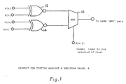
- the circuit of figure 1 may be used.
- This circuit uses eight more transistors than the XOR gate that is required if the Sum is used, but these gates are now not speed critical, and so could be substantially smaller than would previously have been the case.
- a circuit to carry out the invention may comprise two XNOR gates 12, 14 and a MUX 16. Outputs of the XNOR gates are passed to the MUX and the register value R[n-1] determines which to pass to the AND gate. Obviously this is just one means by which the function of this invention can be achieved. As will be apparent to the man skilled in the art other Boolean architectures can be chosen which have the same result.
- the second part of the new circuit takes these results a stage further by indicating what the effect of the incorrect carry value will be. This is achieved by comparing the required 'carry in" at every bit position to produce the target result with the actual carry in. If the carry required to produce the target value is a 1, but the actual carry is a 0 the result will be less than the target value. If the required carry is a 0, but the actual carry is a 1, the result will be more than the target value.
- the comparator will transfer the value of the required carry in (Cinr[n] at the most significant bit position where the ZH values indicate the carry path will not produce the required target value V.
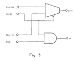
- Figure 3 shows the detail of each block.
- FIG. 3 shows the basic building block for this.
- the Z and H values are used to determine if the sum A+B will be equal to V. If they are not, the value of the required carry-in at the left most failing position determines which is the larger, A+B or V.
- this circuit is significantly faster than performing the addition and then passing the result to a magnitude comparator.
- the number of transistor per bit required for this circuit is constant, and the delay increases only logarithmically.
Description
- This invention relates to improvements in comparator schemes, as carried out in the Arithmetic Logic Unit (ALU) of a microprocessor.
- A typical microprocessor includes the following functional blocks. A central Processing Unit (CPU) which comprises circuitry required to access the appropriate locations in memory and interpret resulting instructions. The execution of the instructions take place in the CPU. The CPU contains the Arithmetic Logic Unit (ALU), a control section, various registers etc.. The exact content of the CPU will obviously vary depending on the application of the microprocessor. The ALU is a combinational network that performs arithmetic and logical operations on data. Typical operations which are carried out include adding, subtracting, multiplying, dividing and comparing operations.
- In operation, the speed of the processor is dependent on the speed of operation of any of the individual blocks within the processor. In addition there is constant effort being undertaken to make the components of the processor both smaller and less speed critical.
- Certain methods have been proposed to determine whether the sum of two numbers will be equal to a third. One such method is disclosed in our European
patent application No 0 679 989 (TIL-17549 GB). In this method the sum of two or more variables is compared with a predetermined constant value. A test is carried out which confirms that the sum is either equal to or not equal to the constant value. - One problem with this method is that if the test confirms that the sum is not equal to the constant there is no way of knowing which is larger than the other. There are methods which determine the larger of two numbers but this obviously causes a delay and requires more hardware.
- European Patent Application No. 0 328 871 discloses a method of determining whether the sum of two numbers is equal to zero and, if not, which of the two numbers is the larger by performing a digit by digit comparison of the two numbers.
- One object of the present invention is to provide a method which tests whether the sum of two variables is equal to, greater than or smaller than a third variable with one simple test.
- The invention provides a method of operation of a comparator capable of comparing the sum of two binary variables A and B with a third binary variable V, including the steps of:
- deriving a set of values Cinr where Cinr[n] = V[n] xor P[n], where V[n] is the nth digit of the third variable V and P[n] is a value P[n] = A[n] xor B[n], A[n] and B[n] being the digits of A and B at the position n and xor being the eXclusive OR logic function,
- deriving a set of values ZH, where
ZH[n] = Z[n] if V[n] = 0 and V[n-1] = 0,
ZH[n] = ∼H[n] if V[n] = 0 and V[n-1] = 1,
ZH[n] = ∼Z[n] if V[n] = 1 and V[n-1] = 0,
ZH[n] = H[n] if V[n] = 1 and V[n-1] = 1, where
"∼" indicates the complement of a value,
H[n] = P[n] xor G[n-1] and Z[n] = P[n] xor K[n-1] according to the following: - G[n-1] is 1 only if the digits A[n-1] and B[n-1] at the position n-1 in the variables A and B are both 1,
- K[n-1] is 1 only if the digits A[n-1] and B[n-1] at the position n-1 in the variables A and B are both 0 and
- determining the result of the comparison by selecting the value of Cinr which corresponds to the most significant 0 of the value of ZH, one value of the selected Cinr indicating whether or not A+B<V.
-
- Preferably, the step of determining the result of the comparison includes:
- combining adjacent pairs of Cinr and ZH (Cinr[n], ZH[n], Cinr[n-1],
ZH[n-1]) and reducing each pair to a single Cinr[out] and ZH[out] in accordance with:
- if ZH[n] is 0, then Cinr[n] becomes Cinr[out] and ZH[out] is 0 and,
- if ZH[n] is 1 and ZH[n-1] is 0, then Cinr[n-1] becomes C[out] and ZH[out] is 0,
- if both ZH[n] and ZH[n-1] are 1, C[out] having a "don't care" condition, this being
indicated by ZH[out] being 1,
combining adjacent pairs of Cinr[out] and ZH[out] and so reduced and reducing the adjacent values to a succeeding set in accordance with the above rules and
continuing the combine-and-reduce steps until a single Cinr and ZH pair is obtained. -
- Preferably, the method includes the step of providing an output indicating that A+B=V when all of the values of ZH are 1.
- The invention also provides a comparator capable of indicating whether A+B<V, where A, B and V are binary variables including:
- means for deriving a set of values Cinr where Cinr[n] = V[n] xor P[n], where V[n] is the nth digit of the third variable V and P[n] is a value P[n] = A[n] xor B[n], A[n] and B[n] being the digits of A and b at the position n and xor being the eXclusive OR logic function,
- means for deriving a set of values ZH, where
ZH[n] = Z[n] if V[n] = 0 and V[n-1] = 0,
ZH[n] = ∼H[n] if V[n] = 0 and V[n-1] = 1,
ZH[n] = ∼Z[n] if V[n] = 1 and V[n-1] = 0,
ZH[n] = H[n] if V[n] = 1 and V[n-1] = 1, where
"∼" indicates the complement of a value,
H[n] = P[n] xor G[n-1] and Z[n] = P[n] xor K[n-1] according to the following: - G[n-1] is 1 only if the digits A[n-1] and B[n-1] at the position n-1 in the variables A and B are both 1,
- K[n-1] is 1 only if the digits A[n-1] and B[n-1] at the position n-1 in the variables A and B are both 0 and
- means for determining the result of the comparison by selecting the value of Cinr which corresponds to the most significant 0 of the value of ZH, one value of the selected Cinr indicating whether or not A+B<V.
-
- Preferably, the means for determining the result of the comparison includes:
- a first set of means for receiving and combining adjacent pairs of Cinr and ZH
(Cinr[n], ZH[n], Cinr[n-1], ZH[n-1]) and reducing each pair to a single Cinr[out] and
ZH[out] in accordance with:
- if ZH[n] is 0, then Cinr[n] becomes Cinr[out] and ZH[out] is 0, and,
- if ZH[n] is 1 and ZH[n-1] is 0, then Cinr[n-1] becomes C[out] and ZH[out] is 0,
- if both ZH[n] and ZH[n-1] are 1, C[out] having a "don't care" condition, this being indicated by ZH[out] being 1,
- a second set of means for receiving and combining adjacent pairs of Cinr and ZH connected to receive Cinr[out] and ZH[out] for reducing the adjacent values to a succeeding set in accordance with the above rules and
- as many further sets of means connected to receive Cinr and ZH values from the previous means for continuing the combine-and-reduce steps as required to obtain a single Cinr and ZH.
-
- Preferably, each of said means for selecting the value of Cinr which corresponds to the most significant 0 of the value of ZH includes a multiplexer and an AND gate, the multiplexer being connected to receive Cinr[n] and Cinr[n-1] as inputs and ZH[n] as a control signal and the AND gate being connected to receive ZH[n] and ZH[n-1] as inputs.
- Preferably, the comparator includes means capable of providing an output indicating that A+B=V when all of the values of ZH are 1.
- Preferably, the means for deriving a ZH value includes a multiplexer which, in operation, provides the ZH value at an output terminal, a first exclusive-nor gate connected to receive V[n] and Z[n] as input values and connected to supply its output signal to a first input terminal of the multiplexer, a second exclusive-nor gate connected to receive ∼V[n] and H[n] as input values and connected to supply its output signal to a second input terminal of the multiplexer, a control terminal of the multiplexer being connected to receive V[n-1].
- Advantageously, an arithmetic and logic unit (ALU) includes a comparator in accordance with the invention.
- This has the advantage that it is possible to determine whether the sum is equal to, greater than or smaller than the third variable.
- Reference will now be made, by way of example, to the accompanying drawings, in which:
- Figure 1 is a diagram of one part of the circuit of the invention,
- Figure 2 is a diagram of the structure position of a magnitude comparator according to the present invention; and
- Figure 3 is a diagram of the functions included in each block of the Figure 2 structure.
-
- The invention is concerned with identifying the value of the sum of A and B relative to a predetermined value V.
- The first part of the new circuit is based on the method for performing an A+B=V test. This relies on comparing the possible carry values with those required to produce the correct target result. It checks if there are any occurrences where the carry path cannot have the value required to produce the sum. If there are no occurrences then A+B equals V. If there are occurrences, then A+B does not equal V. The following is one method by which the method operates.
- The INPUTS to the carry ripple portion of an adder at any bit position [n] can be represented using three MUTUALLY EXCLUSIVE variables, namely:-
P[n] Propagate, Cout=Cin When adding 1+0, or 0+1; G[n] Generate, Cout=1 When adding 1+1; and K[n] Kill, Cout=0 When adding 0+0. - Sum[n]=P[n] xor Cout[n-1].
- If P[n-1] is false, then Cout[n-1] is known and so Sum[n] can be determined with certainty. If P[n-1] is true, then Cout[n-1] is not known and so Sum[n] is not known. But, if P[n] is also true then Sum[n] will be the same as Sum[n-1]. Or, if P[n] is false then Sum[n] will be the opposite to Sum[n-1].
- From this it can be seen that examination of P[n,n-1], G[n,n-1] and K[n,n-1] will lead to four possible conditions:-
- 1 Sum[n]=O;
- 2 Sum[n]=l;
- 3 Sum[n]=Sum[n-1]; and
- 4 Sum[n]=∼Sum[n-1].
-
- From this information it is possible to make further assumptions. If P[n-l]=0 for a certain Sum[n]=O, then:-
- P[n]=l and G[n-1]=1; and/or
- P[n]=0 and K[n-1]=1.
-
- Similarly if P[n-1]=0 for a certain Sum[n]=l, then:-
- P[n]=0 and G[n-l]=1; and/or
- P[n]=l and K[n-1]=1.
-
- It further follows that if P[n-l]=l for Sum[n]=Sum[n-1] then P[n]=l and for Sum[n]=∼Sum[n-1] then P[n]=0
- As can be seen, EITHER the Sum is known, OR the relationship to the previous bit is known. If the full result of the ADD is known, all that is required to test if the answer is the required value, is for each bit to say if it is correct, (i.e. invert if testing for zero, pass if testing for 1), and put these into a wide fast parallel AND gate.
- This method does not wait on the SUM at each bit to be available, but considers overlapping pairs. The TEST at each bit is a double test, EITHER Sum[n] is known, and it is correct, OR IF Sum[n] is not known, its relationship to Sum[n-1] must be correct. If the double test PASSES at EVERY bit position the answer WILL be the required result. If this double test FAILS at ANY bit position the result WILL NOT be the required result.
- If the target result is 00 i.e., we want to know if Sum[n]=O and Sum [n-l]=0 then EITHER Sum[n]=O, OR Sum[n]=Sum[n-1] which yields the following:-
P[n]=l and G[n-l]=l Sum[n]=O; P[n]=O and K[n-l]=l Sum[n]=O; and P[n]=l and P[n-l]=l Sum[n]=Sum[n-1]. - If the target result is 01 i.e., we want to know if Sum[n]=O and Sum[n-l]=1 then EITHER Sum[n]=O, OR Sum[n]=∼Sum[n-1] which yields the following:-
P[n]=l and G[n-l]=l Sum[n]=O; P[n]=O and K[n-l]=l Sum[n]=O; and P[n]=O and P[n-l]=l Sum[n]=∼Sum[n-1]. - If the target result is 10 i.e., we want to know if Sum[n]=l and Sum [n-l]=0 then EITHER Sum[n]=l, OR Sum[n]=∼Sum[n-1] which yields the following:-
P[n]=O and G[n-l]=l Sum[n]=l; P[n]=l and K[n-l]=l Sum[n]=l; P[n]=0 and P[n-l]=l Sum[n]=∼Sum[n-1]. - If the target result is 11 i.e., we want to know if Sum[n]=l and Sum[n-l]=1 then EITHER Sum[n]=l, OR Sum[n]=Sum[n-1] which yields the following:-
P[n]=O and G[n-l]=l Sum[n]=1; P[n]=l and K[n-l]=l Sum[n]=1; and P[n]=l and P[n-l]=l Sum[n]=Sum[n-1]. - If we create two new variables, i.e.:-
- P[n] xor K[n-l]=Z[n]; and
- P[n] xor G[n-l]=H[n], then the 00 test is Z[n], the 01 test is
∼H[n], the 10 test is ∼Z[n] and the 11 test is H[n]. The test
for bit zero is slightly different. Here it is necessary to
test for a 1 with P[0] xor cin; and test for a 0 with
P[0] xor ∼cin. (i.e. evaluate it). The table below illustrates this.
-
- One way of implementing all this is to build 2 extra xor gates per ALU bit, and create the Z[n] and H[n] terms. These are then used, as appropriate, as inputs to a wide AND gate to detect any required value. This is very simple for a constant, for example C.
- To compare against a register value, R, the circuit of figure 1 may be used. This circuit uses eight more transistors than the XOR gate that is required if the Sum is used, but these gates are now not speed critical, and so could be substantially smaller than would previously have been the case. As can be seen from the figure a circuit to carry out the invention may comprise two
XNOR gates MUX 16. Outputs of the XNOR gates are passed to the MUX and the register value R[n-1] determines which to pass to the AND gate. Obviously this is just one means by which the function of this invention can be achieved. As will be apparent to the man skilled in the art other Boolean architectures can be chosen which have the same result. - The second part of the new circuit takes these results a stage further by indicating what the effect of the incorrect carry value will be. This is achieved by comparing the required 'carry in" at every bit position to produce the target result with the actual carry in. If the carry required to produce the target value is a 1, but the actual carry is a 0 the result will be less than the target value. If the required carry is a 0, but the actual carry is a 1, the result will be more than the target value.
- Within an addition it is quite possible for there to be many places where the required carry and the actual carry differ. It is necessary to use the difference with the most significant bit (MSB) position to determine the result of the A+B>=V test. This is where the conventional (A>=B) magnitude comparator is used. A simple two operand magnitude comparator finds the most significant bit position where the two operands are different and this is used to say if A>B or B>A. (If, at this position, A[n]= 1 and B[n]=O then A>B, or, ir A[n]=O and B[n]=l then B>A.
- The required carry in (Cinr[n]) is easy to determine. The result at any position is Sum[n] = P[n] xor Cin[n], where Cina[n] is the actual carry in. From this, it can be seen that the required carry in Cinr[n] = P[n] xor V[n] .
- Referring to Figure 2, in this case the comparator will transfer the value of the required carry in (Cinr[n] at the most significant bit position where the ZH values indicate the carry path will not produce the required target value V. Figure 3 shows the detail of each block.
- If ZH[n] = 0, then the corresponding Cinr[n] is irrelevant. Only if ZH[n] = 1 is Cinr[n] relevant, and then the value of Cinr which corresponds to the most significant zero of ZH[n] is the one that determines the result.
- The method shown in Figures 2 and 3 is a way of transferring to the output value of Cinr[n] which corresponds to the most significant zero of ZH[n].
- For example:
n 7 6 5 4 3 2 1 0 Cinr 0 1 0 0 1 0 1 0 ZH 1 1 0 1 0 1 0 1 * In this case ZH[5] is the most significant zero and so Cinr[5](0) must be transferred to the output - For example:
n 7 6 5 4 3 2 1 0 Cinr 0 1 0 0 1 0 1 0 ZH 1 1 1 1 0 1 0 1 * In this case ZH[3] is the most significant zero and so Cinr[3](1) must be transferred to the output - Figure 3 shows the basic building block for this.
- 2 adjacent input values of Cinr and ZH are combined and reduced to a single set of Cinr(out) and ZH(out) in the following manner. If both ZH inputs are 1, then both Cinr[0] and Cinr[l] are irrelevant and this is indicated by ZH(out) also being a l. (The AND gates does this).
If ZH[1] = 0 then Cinr[l] is the value which determines Cinr(out) and so it is transferred to the output. If ZH[1] = 1 then Cinr[0] will be transferred to the output. (The MUX does this). - This can be summarized as follows:
ZH[1] ZH[0] ZH[out] transfer 0 0 0 Cinr[1] 0 1 0 Cinr[1] 1 0 0 Cinr[0] 1 1 1 Cinr[0] - The last case where ZH[1] = ZH[0] = 1, the transfer out is actually a 'don't care'.
- Figure 2 shows how the basic building block is recursively combined in order to keep reducing the number of terms until eventually there is only a single ZH (the AND of all input ZH's) and a single Cinr which has come from the most significant ZH[n]=O, if there is one.
- The Z and H values are used to determine if the sum A+B will be equal to V. If they are not, the value of the required carry-in at the left most failing position determines which is the larger, A+B or V.
- The advantages are that this circuit is significantly faster than performing the addition and then passing the result to a magnitude comparator. The number of transistor per bit required for this circuit is constant, and the delay increases only logarithmically.
- required carry in is 0, therefore A+B >V

- required carry in is 1, therefore A+B < V

Claims (9)
- A method of operation of a comparator capable of comparing the sum of two binary variables A and B with a third binary variable V, including the steps of:deriving a set of values Cinr where Cinr[n] = V[n] xor P[n], where V[n] is the nth digit of the third variable V and P[n] is a value P[n] = A[n] xor B[n], A[n] and B[n] being the digits of A and B at the position n and xor being the eXclusive OR logic function,deriving a set of values ZH, where
ZH[n] = Z[n] if V[n] = 0 and V[n-1] = 0,
ZH[n] = ∼H[n] if V[n] = 0 and V [n-1] = 1,
ZH[n] = ∼Z[n] if V[n] = 1 and V[n-1] = 0,
ZH[n] = H[n] if V[n] = 1 and V[n-1] = 1, where
"∼" indicates the complement of a value,
H[n] = P[n] xor G[n-1] and Z[n] = P[n] xor K[n-1] according to the following:G[n-1] is 1 only if the digits A[n-1] and B[n-1] at the position n-1 in the variables A andB are both 1,K[n-1] is 1 only if the digits A[n-1] and B[n-1] at the position n-1 in the variables A andB are both 0 anddetermining the result of the comparison by selecting the value of Cinr which corresponds to the most significant 0 of the value of ZH, one value of the selected Cinr indicating whether or not A+B<V. - A method as claimed in claim 1, wherein the step of determining the result of the comparison includes:combining adjacent pairs of Cinr and ZH (Cinr[n], ZH[n], Cinr[n-1], ZH[n-1]) and reducing each pair to a single Cinr[out] and ZH[out] in accordance with:if ZH[n] is 0 , then Cinr[n] becomes Cinr[out] and ZH[out] is 0 and,if ZH[n] is 1 and ZH[n-1] is 0, then Cinr[n-1] becomes C[out] and ZH[out] is 0,if both ZH[n] and ZH[n-1] are 1, C[out] having a "don't care" condition, this being indicated by ZH[out] being 1,combining adjacent pairs of Cinr[out] and ZH[out] and so reduced and reducing the adjacent values to a succeeding set in accordance with the above rules andcontinuing the combine-and-reduce steps until a single Cinr and ZH pair is obtained.
- A method as claimed in claim 1 or claim 2, including the step of providing an output indicating that A+B=V when all of the values of ZH are 1.
- A comparator capable of indicating whether A+B<V, where A, B and V are binary variables including:means for deriving a set of values Cinr where Cinr[n] = V[n] xor P[n], where V[n] is the nth digit of the third variable V and P[n] is a value P[n] = A[n] xor B[n], A[n] and B[n] being the digits of A and b at the position n and xor being the eXclusive OR logic function,means (12, 14, 16) for deriving a set of values ZH, where
ZH[n] = Z[n] if V[n] = 0 and V[n-1] = 0,
ZH[n] = ∼H[n] if V[n] = 0 and V[n-1] = 1,
ZH[n] = ∼Z[n] if V[n] = 1 and V[n-1] = 0,
ZH[n] = H[n] if V[n] = 1 and V[n-1] = 1, where
"∼" indicates the complement of a value,
H[n] = P[n] xor G[n-1] and Z[n] = P[n] xor K[n-1] according to the following:G[n-1] is 1 only if the digits A[n-1] and B[n-1] at the position n-1 in the variables A andB are both 1,K[n-1] is 1 only if the digits A[n-1] and B[n-1] at the position n-1 in the variables A and B are both 0 andmeans for determining the result of the comparison by selecting the value of Cinr which corresponds to the most significant 0 of the value of ZH, one value of the selected Cinr indicating whether or not A+B<V. - A comparator as claimed in claim 4, wherein the means for determining the result of the comparison includes:a first set of means (1, 3, 5...31) for receiving and combining adjacent pairs of Cinr and ZH (Cinr[n], ZH[n], Cinr[n-1], ZH[n-1]) and reducing each pair to a single Cinr[out] and ZH[out] in accordance with:if ZH[n] is 0, then Cinr[n] becomes Cinr[out] and ZH[out] is 0, and,if ZH[n] is 1 and ZH[n-1] is 0, then Cinr[n-1] becomes C[out] and ZH[out] is 0,if both ZH[n] and ZH[n-1] are 1, C[out] having a "don't care" condition, this being indicated by ZH[out] being 1,a second set of means (2, 6, 10... 30) for receiving and combining adjacent pairs of Cinr and ZH connected to receive Cinr[out] and ZH[out] for reducing the adjacent values to a succeeding set in accordance with the above rules andas many further sets of means (8, 16, 24) connected to receive Cinr and ZH values from the previous means for continuing the combine-and-reduce steps as required to obtain a single Cinr and ZH.
- A comparator as claimed in claim 4 or claim 5, wherein each of said means for selecting the value of Cinr which corresponds to the most significant 0 of the value of ZH includes a multiplexer and an AND gate, the multiplexer being connected to receive Cinr[n] and Cinr[n-1] as inputs and ZH[n] as a control signal and the AND gate being connected to receive ZH[n] and ZH[n-1] as inputs.
- A comparator as claimed in any one of claims 4 to 6, including means capable of providing an output indicating that A+B=V when all of the values of ZH are 1.
- A comparator as claimed in any one of claims 4 to 7, wherein the means for deriving a ZH value includes a multiplexer which, in operation, provides the ZH value at an output terminal, a first exclusive-nor gate connected to receive V[n] and Z[n] as input values and connected to supply its output signal to a first input terminal of the multiplexer, a second exclusive-nor gate connected to receive ∼V[n] and H[n] as input values and connected to supply its output signal to a second input terminal of the multiplexer, a control terminal of the multiplexer being connected to receive V[n-1].
- An arithmetic and logic unit (ALU) including a comparator as claimed in any one of claims 4 to 8.
Applications Claiming Priority (2)
| Application Number | Priority Date | Filing Date | Title |
|---|---|---|---|
| GB9419614A GB2293665A (en) | 1994-09-29 | 1994-09-29 | A look-ahead scheme. |
| GB9419614 | 1994-09-29 |
Publications (3)
| Publication Number | Publication Date |
|---|---|
| EP0704793A2 EP0704793A2 (en) | 1996-04-03 |
| EP0704793A3 EP0704793A3 (en) | 1996-05-01 |
| EP0704793B1 true EP0704793B1 (en) | 2002-05-08 |
Family
ID=10762062
Family Applications (1)
| Application Number | Title | Priority Date | Filing Date |
|---|---|---|---|
| EP95306861A Expired - Lifetime EP0704793B1 (en) | 1994-09-29 | 1995-09-28 | Method and circuit to compare the sum of two numbers to a third number |
Country Status (5)
| Country | Link |
|---|---|
| US (1) | US5739745A (en) |
| EP (1) | EP0704793B1 (en) |
| JP (1) | JP3696669B2 (en) |
| DE (1) | DE69526618T2 (en) |
| GB (1) | GB2293665A (en) |
Families Citing this family (1)
| Publication number | Priority date | Publication date | Assignee | Title |
|---|---|---|---|---|
| KR100305679B1 (en) * | 1999-02-24 | 2001-09-26 | 윤종용 | Test method of tester of a semiconductor memory device and apparatus thereof |
Family Cites Families (7)
| Publication number | Priority date | Publication date | Assignee | Title |
|---|---|---|---|---|
| DE191452C (en) * | ||||
| NL297219A (en) * | 1962-08-29 | 1900-01-01 | ||
| EP0191452B1 (en) * | 1985-02-11 | 1989-05-10 | Siemens Aktiengesellschaft | Method and circuit for monitoring the sum or difference of two quantities by comparison with a third quantity in a binary representation |
| US4737926A (en) * | 1986-01-21 | 1988-04-12 | Intel Corporation | Optimally partitioned regenerative carry lookahead adder |
| US4924422A (en) * | 1988-02-17 | 1990-05-08 | International Business Machines Corporation | Method and apparatus for modified carry-save determination of arithmetic/logic zero results |
| US4935719A (en) * | 1989-03-31 | 1990-06-19 | Sgs-Thomson Microelectronics, Inc. | Comparator circuitry |
| US5528181A (en) * | 1994-11-02 | 1996-06-18 | Advanced Micro Devices, Inc. | Hazard-free divider circuit |
-
1994
- 1994-09-29 GB GB9419614A patent/GB2293665A/en not_active Withdrawn
-
1995
- 1995-09-28 DE DE69526618T patent/DE69526618T2/en not_active Expired - Lifetime
- 1995-09-28 JP JP25146595A patent/JP3696669B2/en not_active Expired - Fee Related
- 1995-09-28 EP EP95306861A patent/EP0704793B1/en not_active Expired - Lifetime
-
1997
- 1997-03-04 US US08/811,333 patent/US5739745A/en not_active Expired - Lifetime
Also Published As
| Publication number | Publication date |
|---|---|
| US5739745A (en) | 1998-04-14 |
| DE69526618D1 (en) | 2002-06-13 |
| JP3696669B2 (en) | 2005-09-21 |
| DE69526618T2 (en) | 2002-10-31 |
| GB9419614D0 (en) | 1994-11-16 |
| EP0704793A2 (en) | 1996-04-03 |
| JPH08185310A (en) | 1996-07-16 |
| GB2293665A (en) | 1996-04-03 |
| EP0704793A3 (en) | 1996-05-01 |
Similar Documents
| Publication | Publication Date | Title |
|---|---|---|
| US5317527A (en) | Leading one/zero bit detector for floating point operation | |
| EP0585619B1 (en) | Method of detecting zero condition of arithmetic or logical computation result, and circuit for same | |
| US5586069A (en) | Arithmetic logic unit with zero sum prediction | |
| JP3589719B2 (en) | Efficient hardware handling of positive and negative overflows resulting from arithmetic operations | |
| EP0127988B1 (en) | A normalizing circuit | |
| JPH0542011B2 (en) | ||
| EP0136174B1 (en) | Enhanced alu test hardware | |
| EP0328619B1 (en) | Apparatus and method for using a single carry chain for leading one detection and for ''sticky'' bit calculation | |
| US4811272A (en) | Apparatus and method for an extended arithmetic logic unit for expediting selected floating point operations | |
| US8370415B2 (en) | Overflow detection and clamping with parallel operand processing for fixed-point multipliers | |
| US6499044B1 (en) | Leading zero/one anticipator for floating point | |
| US4947359A (en) | Apparatus and method for prediction of zero arithmetic/logic results | |
| US5867413A (en) | Fast method of floating-point multiplication and accumulation | |
| US6629118B1 (en) | Zero result prediction | |
| EP0704793B1 (en) | Method and circuit to compare the sum of two numbers to a third number | |
| JPH04350724A (en) | Shift extent detecting circuit | |
| US5644521A (en) | Comparator scheme | |
| EP0762268A1 (en) | Apparatus and method to determine a most significant digit | |
| JPS6051728B2 (en) | High-speed calculation processing method | |
| US4914579A (en) | Apparatus for branch prediction for computer instructions | |
| EP0313817B1 (en) | Method and apparatus for explicitly evaluating conditions in a data processor | |
| US6272514B1 (en) | Method and apparatus for interruption of carry propagation on partition boundaries | |
| US6301597B1 (en) | Method and apparatus for saturation in an N-NARY adder/subtractor | |
| KR0175358B1 (en) | Status Flag Detection Circuit of Computer for High Speed | |
| JPH03105615A (en) | Composite arithmetic circuit of multiplication and addition provided with maximum value or minimum value detecting function |
Legal Events
| Date | Code | Title | Description |
|---|---|---|---|
| PUAI | Public reference made under article 153(3) epc to a published international application that has entered the european phase |
Free format text: ORIGINAL CODE: 0009012 |
|
| PUAL | Search report despatched |
Free format text: ORIGINAL CODE: 0009013 |
|
| AK | Designated contracting states |
Kind code of ref document: A2 Designated state(s): DE FR GB IT NL |
|
| RTI1 | Title (correction) | ||
| RTI1 | Title (correction) | ||
| AK | Designated contracting states |
Kind code of ref document: A3 Designated state(s): DE FR GB IT NL |
|
| 17P | Request for examination filed |
Effective date: 19961014 |
|
| 17Q | First examination report despatched |
Effective date: 20000204 |
|
| GRAG | Despatch of communication of intention to grant |
Free format text: ORIGINAL CODE: EPIDOS AGRA |
|
| GRAG | Despatch of communication of intention to grant |
Free format text: ORIGINAL CODE: EPIDOS AGRA |
|
| GRAH | Despatch of communication of intention to grant a patent |
Free format text: ORIGINAL CODE: EPIDOS IGRA |
|
| REG | Reference to a national code |
Ref country code: GB Ref legal event code: IF02 |
|
| GRAH | Despatch of communication of intention to grant a patent |
Free format text: ORIGINAL CODE: EPIDOS IGRA |
|
| GRAA | (expected) grant |
Free format text: ORIGINAL CODE: 0009210 |
|
| AK | Designated contracting states |
Kind code of ref document: B1 Designated state(s): DE FR GB IT NL |
|
| PG25 | Lapsed in a contracting state [announced via postgrant information from national office to epo] |
Ref country code: NL Free format text: LAPSE BECAUSE OF FAILURE TO SUBMIT A TRANSLATION OF THE DESCRIPTION OR TO PAY THE FEE WITHIN THE PRESCRIBED TIME-LIMIT Effective date: 20020508 Ref country code: IT Free format text: LAPSE BECAUSE OF FAILURE TO SUBMIT A TRANSLATION OF THE DESCRIPTION OR TO PAY THE FEE WITHIN THE PRE;WARNING: LAPSES OF ITALIAN PATENTS WITH EFFECTIVE DATE BEFORE 2007 MAY HAVE OCCURRED AT ANY TIME BEFORE 2007. THE CORRECT EFFECTIVE DATE MAY BE DIFFERENT FROM THE ONE RECORDED.SCRIBED TIME-LIMIT Effective date: 20020508 |
|
| REF | Corresponds to: |
Ref document number: 69526618 Country of ref document: DE Date of ref document: 20020613 |
|
| NLV1 | Nl: lapsed or annulled due to failure to fulfill the requirements of art. 29p and 29m of the patents act | ||
| ET | Fr: translation filed | ||
| PLBE | No opposition filed within time limit |
Free format text: ORIGINAL CODE: 0009261 |
|
| STAA | Information on the status of an ep patent application or granted ep patent |
Free format text: STATUS: NO OPPOSITION FILED WITHIN TIME LIMIT |
|
| 26N | No opposition filed |
Effective date: 20030211 |
|
| PGFP | Annual fee paid to national office [announced via postgrant information from national office to epo] |
Ref country code: GB Payment date: 20100809 Year of fee payment: 16 |
|
| PGFP | Annual fee paid to national office [announced via postgrant information from national office to epo] |
Ref country code: DE Payment date: 20100930 Year of fee payment: 16 |
|
| REG | Reference to a national code |
Ref country code: FR Ref legal event code: ST Effective date: 20110531 |
|
| PG25 | Lapsed in a contracting state [announced via postgrant information from national office to epo] |
Ref country code: FR Free format text: LAPSE BECAUSE OF NON-PAYMENT OF DUE FEES Effective date: 20100930 |
|
| PGFP | Annual fee paid to national office [announced via postgrant information from national office to epo] |
Ref country code: FR Payment date: 20090916 Year of fee payment: 15 |
|
| GBPC | Gb: european patent ceased through non-payment of renewal fee |
Effective date: 20110928 |
|
| REG | Reference to a national code |
Ref country code: DE Ref legal event code: R119 Ref document number: 69526618 Country of ref document: DE Effective date: 20120403 |
|
| PG25 | Lapsed in a contracting state [announced via postgrant information from national office to epo] |
Ref country code: DE Free format text: LAPSE BECAUSE OF NON-PAYMENT OF DUE FEES Effective date: 20120403 |
|
| PG25 | Lapsed in a contracting state [announced via postgrant information from national office to epo] |
Ref country code: GB Free format text: LAPSE BECAUSE OF NON-PAYMENT OF DUE FEES Effective date: 20110928 |