EP0704787B1 - Circuit for eliminating glitches from a series of clock pulses - Google Patents
Circuit for eliminating glitches from a series of clock pulses Download PDFInfo
- Publication number
- EP0704787B1 EP0704787B1 EP95113633A EP95113633A EP0704787B1 EP 0704787 B1 EP0704787 B1 EP 0704787B1 EP 95113633 A EP95113633 A EP 95113633A EP 95113633 A EP95113633 A EP 95113633A EP 0704787 B1 EP0704787 B1 EP 0704787B1
- Authority
- EP
- European Patent Office
- Prior art keywords
- output
- pulse
- circuit
- potential
- input
- Prior art date
- Legal status (The legal status is an assumption and is not a legal conclusion. Google has not performed a legal analysis and makes no representation as to the accuracy of the status listed.)
- Expired - Lifetime
Links
Images

Classifications
-
- H—ELECTRICITY
- H03—ELECTRONIC CIRCUITRY
- H03K—PULSE TECHNIQUE
- H03K5/00—Manipulating of pulses not covered by one of the other main groups of this subclass
- H03K5/125—Discriminating pulses
- H03K5/1252—Suppression or limitation of noise or interference
Definitions
- the invention relates to a circuit arrangement for interference-freeing a clock signal pulse sequence from disturbances occurring with the pulse edges.
- this clock is generated or fed in at a central location and distributed via a clock distribution system, which may have considerable line lengths.
- a clock distribution system which may have considerable line lengths.
- faults can be masked out by clocking the data signals, e.g. by the information being recorded by the receivers with the negative clock edge, so that the disturbances arising with the positive clock edge have already subsided at the time of transfer.
- this method cannot be used for the clock itself and for a pulse frame signal derived from it, which is used as a synchronization signal for the units of the data processing system.
- the distribution network for clock and synchronization pulses has been made insensitive to interference by appropriate decoupling measures in cases of such data processing systems, or by using interference-sensitive reception gates to avoid the effects of interference.
- the object of the invention is therefore to provide a circuit arrangement with which clock pulse sequences which are disturbed in the manner mentioned are freed from disturbances in order to be able to ensure proper data processing operation with comparatively little outlay.
- a circuit arrangement according to the solution to this problem has the features specified in the characterizing part of patent claim 1.
- the circuit arrangement according to the invention therefore has the effect that an edge change occurring after a pulse pause, regardless of whether it is to be regarded as a fault because the full signal value is not achieved thereby or whether it represents an undisturbed pulse edge, leads to a potential jump on the output side. which represents an undisturbed impulse.
- Potential changes occurring within the predefined time span have no effect.
- Further edge changes following an edge change at the end of the pulse also have no effect if they lie within the predefined time.
- a special embodiment of the circuit arrangement according to the invention is characterized in a subclaim.
- a circuit arrangement for interference-freeing of the pulse frame or synchronization signal mentioned is the subject of another patent application.
- Figure 1 as an example of the distribution system for clock and synchronization pulses the part of a data processing system in the form of a telephone switching system, which includes such a distribution system.
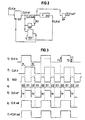
- FIG. 2 shows an embodiment of the circuit arrangement according to the invention.
- Figure 3 is a pulse diagram illustrating the operation of this circuit arrangement.
- FIG. 1 shows a part of a telephone exchange that belongs to its periphery.
- connection modules SLMO-0 to SLMO-3 are shown, to which subscriber lines are to be thought of.
- These line modules contain a corresponding number of subscriber sets, as well as a line group processor.
- connection modules mentioned are part of a larger plurality, which may be 128, for example.
- FIG. 1 also shows a central interface unit I1, via which the data is exchanged with the central parts of the switching center and via which the connection modules are supplied with clock pulses and synchronization signals.
- Distribution units BD0 to BD7 ensure a partially central distribution of data, clock and synchronization signals. They form an interface I2 on the input side and an interface I3 on the output side.
- the output 0 of the part of the interface I3 belonging to the distribution unit BD0 leads, as shown, to the connection modules SLMO-0 to SLMO-3 shown.
- the remaining outputs of this distribution unit or the outputs of the other distribution units lead to further connection modules, not shown here.
- connections of the illustrated distribution network may serve for the distribution of the clock pulse signals.
- Corresponding connections are to be considered for the transmission of the pulse frame signal and the data.
- the circuit shown in FIG. 2 is assigned to the outputs of the distribution units BD0 to BD7, to which it supplies interference-free clock pulses, from where only line connections to the connection modules SLMO-0 to SLMO-3 must be traversed by at most 60 cm, so that disruptive couplings can be avoided here without any special effort. If the clock signals arriving at the connection modules are nevertheless subject to interference, the circuit arrangement according to the invention can also be assigned to its inputs.
- the circuit arrangement according to FIG. 2 has a blocking gate G1, to which the clock pulses, which may be subject to interference, are fed.
- a driver circuit G2 is connected to the output of this blocking gate G1, the output of which is fed back to the input via a resistor R1.
- the output of the blocking gate G1 is also connected to the input of a delay element V, the output of which is connected to the one input of a comparator G3, the other input of which is also connected to the output of the blocking gate G1.
- the output signal of the comparator G3 is fed to the blocking input X of the blocking gate G1.
- Holding circuit which is such that it immediately transfers a potential change at the start and end of the pulse to the output of the circuit arrangement in the form of a potential jump in the amount of the pulse amplitude, regardless of whether the input-side potential change leads to the pulse amplitude being reached or not, if only a threshold value is exceeded. After that, potential changes occurring at its input do not pass on until a certain period of time has elapsed. The time span is dimensioned so that after the end of the impulses occurring at the start and end of the impulse have subsided.
- the holding function could also be generated with the aid of a bistable flip-flop.
- line 1) shows a clock pulse sequence CLKin as it is fed to the blocking gate G1.
- the pulses are shown without interference, in the right part it is shown by way of example that the leading edge of a pulse is subject to interference in such a way that the signal does not yet reach the full amplitude when the edge changes after the pulse pause, and again the value before the edge falls back, see T1, i.e. is faulty and only assumes the correct value after a fault time.
- T2 shows a clock pulse sequence CLKin as it is fed to the blocking gate G1.
- the comparator G3 After the delay time has elapsed, the comparator G3 signals equality again, so that the blocking gate is switched back to the active state and can thus react to an edge change again. Because of the time span, during the disturbances, persistent delay time will be the subsequent falling edge of the pulse.
- resistor R1 is dimensioned such that the potential CLKin * supplied by the now active blocking gate is compared to that occurring at the output of resistor R1 Potential CLKin # can enforce.
Abstract
Description
Die Erfindung betrifft eine Schaltungsanordnung zur Störbefreiung einer Taktsignalimpulsfolge von mit den Impulsflanken auftretenden Störungen.The invention relates to a circuit arrangement for interference-freeing a clock signal pulse sequence from disturbances occurring with the pulse edges.
In Datenverarbeitungsanlagen mit einer Vielzahl von auf der Basis eines Taktsignals arbeitenden Einheiten wird dieser Takt an einer zentralen Stelle erzeugt bzw. eingespeist und über ein Taktverteilsystem verteilt, das unter Umständen beträchtliche Leitungslängen aufweist. Bei einem derartigen Verteilnetz besteht die Gefahr von durch Kopplungen im Augenblick der Umschaltzeitpunkte der Taktsignalimpulse entstehenden Störungen, deren Amplituden die Schaltschwellen von Eingangsschaltungen der Einheiten übersteigen und damit die Gesamtfunktion der Anlage beeinträchtigen.In data processing systems with a large number of units operating on the basis of a clock signal, this clock is generated or fed in at a central location and distributed via a clock distribution system, which may have considerable line lengths. In such a distribution network, there is a risk of interference arising from couplings at the moment of the switching timing of the clock signal pulses, the amplitudes of which exceed the switching thresholds of input circuits of the units and thus impair the overall function of the system.
Soweit hiervon zwischen den Einheiten der Datenverarbeitungsanlage zu übertragende Daten betroffen sind, lassen sich solche Störungen durch Taktung der Datensignale ausblenden, z.B. indem die Informationsaufnahme der Empfänger mit der negativen Taktflanke erfolgt, so daß die mit der positiven Taktflanke entstehenden Störungen zum Übernahmezeitpunkt schon abgeklungen sind.Insofar as this affects data to be transmitted between the units of the data processing system, such faults can be masked out by clocking the data signals, e.g. by the information being recorded by the receivers with the negative clock edge, so that the disturbances arising with the positive clock edge have already subsided at the time of transfer.
Für den Takt selbst und für ein von ihm abgeleitetes Pulsrahmensignal, das als Synchronisiersignal für die Einheiten der Datenverarbeitungsanlage herangezogen wird, kann diese Methode natürlich nicht angewendet werden.Of course, this method cannot be used for the clock itself and for a pulse frame signal derived from it, which is used as a synchronization signal for the units of the data processing system.
Bisher wurde daher in Fällen solcher Datenverarbeitungsanlagen das Verteilnetz für Takt- und Synchronisierimpulse durch entsprechende Entkopplungsmaßnahmen störunempfindlich gemacht, bzw. durch Verwendung von störunempfindlichen Empfangsgattern die Auswirkung von Störungen vermieden.So far, the distribution network for clock and synchronization pulses has been made insensitive to interference by appropriate decoupling measures in cases of such data processing systems, or by using interference-sensitive reception gates to avoid the effects of interference.
Eine solche Lösung erfordert allerdings einen beträchtlichen Aufwand, gegebenenfalls werden auch die Laufzeiten und Laufzeittoleranzen auf dem Verteilsystem zu hoch.However, such a solution requires considerable effort, and the runtimes and runtime tolerances on the distribution system may become too high.
Die Aufgabe der Erfindung besteht daher darin, eine Schaltungsanordnung anzugeben, mit der in der genannten Art gestörte Taktimpulsfolgen von Störungen befreit werden, um mit vergleichsweise geringem Aufwand einen ordnungsgemäßen Datenverarbeitungsbetrieb gewährleisten zu können.The object of the invention is therefore to provide a circuit arrangement with which clock pulse sequences which are disturbed in the manner mentioned are freed from disturbances in order to be able to ensure proper data processing operation with comparatively little outlay.
Eine Schaltungsanordnung gemäß der Lösung dieser Aufgabe weist die im Kennzeichen des Patentanspruchs 1 angegebenen Merkmale auf.A circuit arrangement according to the solution to this problem has the features specified in the characterizing part of
Durch die erfindungsgemäße Schaltungsanordnung ist also bewirkt, daß ein nach einer Impulspause auftretender Flankenwechsel, unabhängig davon, ob er als Störung zu betrachten ist, weil damit der volle Signalwert nicht erreicht wird, oder ob er eine ungestörte Impulsflanke darstellt, ausgangsseitig zu einem Potentialsprung führt, der einen ungestörten Impuls darstellt. Danach innerhalb der vordefinierten Zeitspanne auftretende Potentialwechsel bleiben ohne Auswirkung. Auf einen Flankenwechsel am Impulsende folgende weitere Flankenwechsel wirken sich ebenfalls nicht aus, sofern sie innerhalb der vordefinierten Zeit liegen.The circuit arrangement according to the invention therefore has the effect that an edge change occurring after a pulse pause, regardless of whether it is to be regarded as a fault because the full signal value is not achieved thereby or whether it represents an undisturbed pulse edge, leads to a potential jump on the output side. which represents an undisturbed impulse. Potential changes occurring within the predefined time span have no effect. Further edge changes following an edge change at the end of the pulse also have no effect if they lie within the predefined time.
Eine spezielle Ausgestaltung der erfindungsgemäßen Schaltungsanordnung ist in einem Unteranspruch gekennzeichnet.A special embodiment of the circuit arrangement according to the invention is characterized in a subclaim.
Eine Schaltungsanordnung zur Störbefreiung des erwähnten Pulsrahmen- bzw. Synchronisiersignals ist Gegenstand einer anderen Patentanmeldung.A circuit arrangement for interference-freeing of the pulse frame or synchronization signal mentioned is the subject of another patent application.
Nachstehend wird die Erfindung anhand eines Ausführungsbeispiels unter Bezugnahme auf eine Zeichnung näher erläutert.The invention is explained in more detail below using an exemplary embodiment with reference to a drawing.
In der Zeichnung zeigen:The drawing shows:
Figur 1 als Beispiel für das Verteilsystem für Takt- und Synchronisierimpulse den Teil einer Datenverarbeitungsanlage in Form einer Fernsprechvermittlungsanlage, der ein solches Verteilsystem beinhaltet.Figure 1 as an example of the distribution system for clock and synchronization pulses the part of a data processing system in the form of a telephone switching system, which includes such a distribution system.
Figur 2 ein Ausführungsbeispiel der erfindungsgemäßen Schaltungsanordnung.Figure 2 shows an embodiment of the circuit arrangement according to the invention.
Figur 3 ein den Betrieb dieser Schaltungsanordnung veranschaulichendes Impulsdiagramm.Figure 3 is a pulse diagram illustrating the operation of this circuit arrangement.
In der Figur 1 ist ein Teil einer Fernsprechvermittlungsstelle angedeutet, der deren Peripherie angehört. Es sind vier Anschlußbaugruppen SLMO-0 bis SLMO-3 gezeigt, an die Teilnehmeranschlußleitungen angeschlossen zu denken sind. Diese Anschlußbaugruppen enthalten eine entsprechende Anzahl von Teilnehmersätzen, sowie einen Anschlußgruppenprozessor.FIG. 1 shows a part of a telephone exchange that belongs to its periphery. Four connection modules SLMO-0 to SLMO-3 are shown, to which subscriber lines are to be thought of. These line modules contain a corresponding number of subscriber sets, as well as a line group processor.
Die genannten Anschlußbaugruppen sind Teil einer größeren Mehrzahl, die beispielsweise 128 betragen kann.The connection modules mentioned are part of a larger plurality, which may be 128, for example.
Die Figur 1 zeigt ferner eine zentrale Schnittstelleneinheit I1, über die der Datenaustausch mit den zentralen Teilen der Vermittlungsstelle erfolgt und über die die Anschlußbaugruppen mit Taktimpulsen und Synchronisiersignalen versorgt werden. Verteilereinheiten BD0 bis BD7 sorgen für eine teilzentrale Verteilung von Daten-, Takt- und Synchronisiersignalen. Sie bilden eingangsseitig eine Schnittstelle I2 und ausgangsseitig eine Schnittstelle I3. Der Ausgang 0 des zur Verteilereinheit BD0 gehörigen Teils der Schnittstelle I3 führt, wie dargestellt, zu den gezeigten Anschlußbaugruppen SLMO-0 bis SLMO-3. Die übrigen Ausgänge dieser Verteilereinheit bzw. die Ausgänge der übrigen Verteilereinheiten führen zu hier nicht dargestellten weiteren Anschlußbaugruppen.FIG. 1 also shows a central interface unit I1, via which the data is exchanged with the central parts of the switching center and via which the connection modules are supplied with clock pulses and synchronization signals. Distribution units BD0 to BD7 ensure a partially central distribution of data, clock and synchronization signals. They form an interface I2 on the input side and an interface I3 on the output side. The
Die Verbindungen des dargestellen Verteilernetzes mögen der Verteilung der Taktimpulssignale dienen. Entsprechende Verbindungen sind für die Übertragung des Pulsrahmensignals und der Daten zu denken.The connections of the illustrated distribution network may serve for the distribution of the clock pulse signals. Corresponding connections are to be considered for the transmission of the pulse frame signal and the data.
Die in Figur 2 dargestellte Schaltung ist bei einem Einsatz in einer Anordnung gemäß Figur 1 jeweils den Ausgängen der Verteileinheiten BD0 bis BD7 zugeordnet, an die sie störbefreite Taktimpulse liefert, von wo aus bis zu den Anschlußbaugruppen SLMO-0 bis SLMO-3 nur noch Leitungsverbindungen von höchstens 60 cm zu durchlaufen sind, so daß hier störende Kopplungen ohne besonderen Aufwand vermieden werden können. Sollten die bei den Anschlußbaugruppen ankommenden Taktsignale dennoch störbehaftet sein, so kann die erfindungsgemäße Schaltungsanordnung auch deren Eingängen zugeordnet sein.When used in an arrangement according to FIG. 1, the circuit shown in FIG. 2 is assigned to the outputs of the distribution units BD0 to BD7, to which it supplies interference-free clock pulses, from where only line connections to the connection modules SLMO-0 to SLMO-3 must be traversed by at most 60 cm, so that disruptive couplings can be avoided here without any special effort. If the clock signals arriving at the connection modules are nevertheless subject to interference, the circuit arrangement according to the invention can also be assigned to its inputs.
Eingangsseitig weist die Schaltungsanordnung gemäß Figur 2 ein Sperrgatter G1 auf, dem die unter Umständen störbehafteten Taktimpulse zugeführt werden.On the input side, the circuit arrangement according to FIG. 2 has a blocking gate G1, to which the clock pulses, which may be subject to interference, are fed.
An den Ausgang dieses Sperrgatters G1 ist eine Treiberschaltung G2 angeschlossen, deren Ausgang über einen Widerstand R1 an den Eingang rückgekoppelt ist.A driver circuit G2 is connected to the output of this blocking gate G1, the output of which is fed back to the input via a resistor R1.
Der Ausgang des Sperrgatters G1 steht ferner mit dem Eingang eines Verzögerungsgliedes V in Verbindung, dessen Ausgang mit dem einen Eingang eines Vergleichers G3 verbunden ist, dessen anderer Eingang ebenfalls mit dem Ausgang des Sperrgatters G1 in Verbindung steht. Das Ausgangssignal des Vergleichers G3 wird dem Sperreingang X des Sperrgatters G1 zugeführt.The output of the blocking gate G1 is also connected to the input of a delay element V, the output of which is connected to the one input of a comparator G3, the other input of which is also connected to the output of the blocking gate G1. The output signal of the comparator G3 is fed to the blocking input X of the blocking gate G1.
Die insoweit beschriebene Schaltungsanordnung gemäß Figur 2 bildet, wie nachstehend noch erläutert werden wird, eine Halteschaltung, die so geartet ist, daß sie einen Potentialwechsel am Impulsanfang und am Impulsende unverzögert an den Ausgang der Schaltungsanordnung in Form eines Potentialsprungs in Höhe der Impulsamplitude weitergibt und zwar unabhängig davon, ob der eingangsseitige Potentialwechsel zum Erreichen der Impulsamplitude führt oder nicht, wenn nur ein Schwellwert überschritten wird. Danach an ihrem Eingang auftretende Potentialwechsel gibt sie bis zum Ablauf einer bestimmten Zeitspanne nicht weiter. Die Zeitspanne ist so bemessen, daß nach ihrem Ablauf am Impulsanfang und am Impulsende auftretende Störungen abgeklungen sind. Die Haltefunktion könnte auch mit Hilfe einer bistabilen Kippstufe erzeugt werden.The circuit arrangement according to FIG. 2 described so far forms one, as will be explained below Holding circuit which is such that it immediately transfers a potential change at the start and end of the pulse to the output of the circuit arrangement in the form of a potential jump in the amount of the pulse amplitude, regardless of whether the input-side potential change leads to the pulse amplitude being reached or not, if only a threshold value is exceeded. After that, potential changes occurring at its input do not pass on until a certain period of time has elapsed. The time span is dimensioned so that after the end of the impulses occurring at the start and end of the impulse have subsided. The holding function could also be generated with the aid of a bistable flip-flop.
In Figur 3 zeigt Zeile 1) eine Taktimpulsfolge CLKin, wie sie dem Sperrgatter G1 zugeführt wird. Im linken Teil dieser Zeile sind die Impulse ohne Störungen dargestellt, im rechten Teil ist beispielhaft gezeigt, daß die Vorderflanke eines Impulses in der Weise störbehaftet ist, daß bei dem auf die Impulspause folgenden Flankenwechsel das Signal noch nicht die volle Amplitude erreicht, und wieder auf den Wert vor der Flanke zurückfällt, siehe T1, also gestört ist und erst nach einer Störzeit den korrekten Wert annimmt. Die Abfallflanke ist in der Weise gestört, daß auf sie noch ein kurzer ebenfalls nicht den vollen Signalwert erreichender Impuls, siehe T2, folgt.In FIG. 3, line 1) shows a clock pulse sequence CLKin as it is fed to the blocking gate G1. In the left part of this line the pulses are shown without interference, in the right part it is shown by way of example that the leading edge of a pulse is subject to interference in such a way that the signal does not yet reach the full amplitude when the edge changes after the pulse pause, and again the value before the edge falls back, see T1, i.e. is faulty and only assumes the correct value after a fault time. The falling edge is disturbed in such a way that it is followed by a short pulse that does not reach the full signal value, see T2.
Da nach einer Impulspause, die wesentlich länger als die Verzögerungszeit tv des Verzögerungsgliedes V dauert, an beiden Eingängen des Vergleichers G3 dasselbe der Impulspause entsprechende Potential anliegt, vergleiche Zeile 5), die den Potentialverlauf CLKin* am Ausgang des Sperrgliedes G1 zeigt, mit Zeile 2), in der das Ausgangssignal CLKd des Verzögerungsgliedes dargestellt ist, der Vergleicher also ein das Sperrgatter durchlässig schaltendes Signal liefert, siehe SG3 in Zeile 3, kann ein nachfolgender Flankenwechsel am Eingang des Sperrgatters auf dessen Ausgang durchgreifen. Unabhängig davon, ob dieser Flankenwechsel störbedingt die Impulsamplitude nicht erreicht oder zum der Impulsamplitude entsprechenden Potentialwert führt, erreicht das Ausgangssignal CLKout, siehe Zeile 7) in Figur 3, den vollen Signalwert.Since after a pulse pause that lasts considerably longer than the delay time tv of the delay element V, the same potential corresponding to the pulse pause is present at both inputs of the comparator G3, compare line 5), which shows the potential profile CLKin * at the output of the blocking element G1, with line 2 ), in which the output signal CLKd of the delay element is shown, that is, the comparator delivers a signal that enables the blocking gate to switch, see SG3 in
Dieser Potentialsprung steht sofort am einen Eingang des Vergleichers G3 und auch am Eingang des Verzögerungsgliedes V an, das jedoch nach wie vor als Ausgangssignal das der Impulspause entsprechende Potential an den anderen Vergleichereingang liefert, weswegen der Vergleicher nunmehr Ungleichheit signalisiert, siehe Zeile 3), und dementsprechend das Sperrgatter undurchlässig macht, beispielsweise in einen passiven Tristate-Zustand schaltet. Wie die Zeile 5) zeigt, bestimmt der Ausgang des Sperrgatters G1 nach diesem Potentialsprung den weiteren Signalverlauf zunächst nicht mehr.This potential jump is immediately present at one input of the comparator G3 and also at the input of the delay element V, which, however, continues to deliver the potential corresponding to the pulse pause to the other comparator input as output signal, which is why the comparator now signals inequality, see line 3), and accordingly makes the blocking gate impermeable, for example switches to a passive tristate state. As line 5) shows, the output of the blocking gate G1 no longer determines the further signal curve after this potential jump.
Da der genannte Potentialsprung aber auch an den Eingang der rückgekoppelten Treiberschaltung G2 gelangt ist, wird das erreichte Potential aufrechterhalten, was die Zeile 6) zeigt, in der ein Potentialverlauf CLKin# gezeigt ist, wie er am Ausgangsanschluß des Widerstands R1 auftritt und der mit dem über die Treiberschaltung G4 an den Ausgang der Gesamtschaltungsanordnung weitergegebenen Signalverlauf CLKout übereinstimmt, siehe Zeile 7). In der Zeile 4) ist der Wechsel der Verantwortlichkeit der Ausgänge des Sperrgliedes G1 und des Ausganges des Widerstandes R1 für den Verlauf des von der Schaltunggsanordnung abgegebenen Signals nochmals veranschaulicht. Potentialänderungen, die innerhalb der Verzögerungszeit tv des Verzögerungsgliedes V bzw. während der Zeit auftreten, während der das Sperrgatter G1 sich im Tristate-Zustand befindet, können also ausgangsseitig die Potentialverhältnisse nicht beeinflussen.However, since the potential jump mentioned has also reached the input of the feedback driver circuit G2, the potential achieved is maintained, which is shown in line 6), in which a potential curve CLKin # is shown as it occurs at the output terminal of the resistor R1 and with that via the driver circuit G4 to the output of the overall circuit arrangement corresponds to the signal curve CLKout (see line 7). In line 4) the change in the responsibility of the outputs of the blocking element G1 and the output of the resistor R1 for the course of the signal emitted by the circuit arrangement is illustrated again. Potential changes that occur within the delay time tv of the delay element V or during the time during which the blocking gate G1 is in the tristate state cannot influence the potential conditions on the output side.
Nach Ablauf der Verzögerungszeit signalisiert der Vergleicher G3 wieder Gleichheit, so daß das Sperrgatter wieder in den aktiven Zustand geschaltet wird und damit wieder auf einen Flankenwechsel reagieren kann. Wegen der die Zeitspanne, während der Störungen auftreten können, überdauernden Verzögerungszeit wird es sich dabei um die nachfolgende Abfallflanke des Impulses handeln.After the delay time has elapsed, the comparator G3 signals equality again, so that the blocking gate is switched back to the active state and can thus react to an edge change again. Because of the time span, during the disturbances, persistent delay time will be the subsequent falling edge of the pulse.
Damit es in der dementsprechenden Übergangsphase nicht zu einer Kollision mit dem durch den Treiber G2 über den Widerstand R1 gelieferten Ausgangssignal kommt, ist der Widerstand R1 so bemessen, daß sich das vom nunmehr aktiven Sperrgatter gelieferte Potential CLKin* gegen das am Ausgang des Widerstands R1 auftretende Potential CLKin# durchsetzen kann.So that there is no collision with the output signal supplied by driver G2 via resistor R1 in the corresponding transition phase, resistor R1 is dimensioned such that the potential CLKin * supplied by the now active blocking gate is compared to that occurring at the output of resistor R1 Potential CLKin # can enforce.
Mit diesem letztgenannten Flankenwechsel liegen aber wieder sofort unterschiedliche Potentiale an den Eingängen des Vergleichers G3, womit das Sperrgatter erneut in den passiven Zustand geschaltet wird, mit der Folge, daß Störungen der Rückflanke eines Taktimpulses, siehe T2 in Zeile 1), nicht durchgreifen können. Das dem Vorliegen der Impulspause entsprechende Potential wird von da an bis zum Ablauf der Verzögerungszeit wieder vom rückgekoppelten Treiber G2 bestimmt, erst danach überwiegt wieder die Wirkung des erneut aktiv geschalteten Sperrgatters G1, siehe im Vergleich die Zeilen 4) und 5) der Figur 3.With this last-mentioned edge change, however, there are immediately different potentials at the inputs of the comparator G3, with which the blocking gate is switched to the passive state again, with the result that interference on the trailing edge of a clock pulse, see T2 in line 1), cannot take effect. From then on, the potential corresponding to the presence of the pulse pause is determined again by the feedback driver G2 until the delay time has elapsed; only then does the effect of the blocking gate G1, which has been reactivated again, predominate, see in comparison lines 4) and 5) of FIG. 3.
Claims (2)
- Circuit arrangement for eliminating glitches from a clock-signal pulse train having a predetermined pulse amplitude, the glitches occurring on the pulse edges, characterized in that it comprises a holding circuit to which the clock pulse train is fed and which forwards a sudden potential change which occurs at the start of a pulse and at the end of a pulse, provided that the said sudden potential change exceeds a threshold value, irrespective of its level as a sudden potential change at the level of the pulse amplitude to the circuit output, and maintains the potential value which is then reached, irrespective of the further potential profile at its input, for a predefined time interval after which a glitch which occurs at the start of a pulse and at the end of a pulse has decayed.
- A circuit arrangement according to Claim 1, characterized in that the holding circuit comprises the following component parts:a) a digital inhibit gate (G1), to which the clock pulse train (CLKin) is fed,b) a driver circuit (G2), the input of which is connected directly to the output of the inhibit gate and the output of which is connected via a resistor (R1) to the output of the inhibit gate,c) a delay element (V), which is connected to the output of the inhibit gate and has a delay time which corresponds to the said holding time intervald) a comparator (G3), which, on the input side, is connected to the output of the inhibit gate, on the one hand, and to the output of the delay element, on the other hand, and whose output is connected to the inhibit input (x) of the inhibit gate,and in that an output driver circuit (G4) is provided which forwards the potential respectively present at the output of the inhibit gate as clock pulse signal (CLKout) from which glitches have been removed.
Applications Claiming Priority (2)
| Application Number | Priority Date | Filing Date | Title |
|---|---|---|---|
| DE4434084A DE4434084C1 (en) | 1994-09-23 | 1994-09-23 | Noise elimination circuit for clock pulse sequence |
| DE4434084 | 1994-09-23 |
Publications (2)
| Publication Number | Publication Date |
|---|---|
| EP0704787A1 EP0704787A1 (en) | 1996-04-03 |
| EP0704787B1 true EP0704787B1 (en) | 1997-11-12 |
Family
ID=6529052
Family Applications (1)
| Application Number | Title | Priority Date | Filing Date |
|---|---|---|---|
| EP95113633A Expired - Lifetime EP0704787B1 (en) | 1994-09-23 | 1995-08-30 | Circuit for eliminating glitches from a series of clock pulses |
Country Status (6)
| Country | Link |
|---|---|
| EP (1) | EP0704787B1 (en) |
| AT (1) | ATE160231T1 (en) |
| DE (2) | DE4434084C1 (en) |
| DK (1) | DK0704787T3 (en) |
| ES (1) | ES2109764T3 (en) |
| GR (1) | GR3025434T3 (en) |
Families Citing this family (1)
| Publication number | Priority date | Publication date | Assignee | Title |
|---|---|---|---|---|
| DE10164806B4 (en) * | 2000-09-29 | 2005-03-31 | Agilent Technologies, Inc. (n.d.Ges.d.Staates Delaware), Palo Alto | Delay line control circuit e.g. for high speed reprogrammable delay line for integrated circuit tester, has fine and coarse delay lines to delay input clock signal sequentially |
Family Cites Families (3)
| Publication number | Priority date | Publication date | Assignee | Title |
|---|---|---|---|---|
| EP0309849A1 (en) * | 1987-09-28 | 1989-04-05 | Siemens Aktiengesellschaft | Arrangement for the correction of the pulse length of a digital signal |
| US4988892A (en) * | 1989-06-02 | 1991-01-29 | Atari Corporation | Method and circuit for generating dependent clock signals |
| JPH03224020A (en) * | 1990-01-30 | 1991-10-03 | Fujitsu Ltd | Clock receiving circuit |
-
1994
- 1994-09-23 DE DE4434084A patent/DE4434084C1/en not_active Expired - Fee Related
-
1995
- 1995-08-30 EP EP95113633A patent/EP0704787B1/en not_active Expired - Lifetime
- 1995-08-30 DK DK95113633T patent/DK0704787T3/en active
- 1995-08-30 ES ES95113633T patent/ES2109764T3/en not_active Expired - Lifetime
- 1995-08-30 AT AT95113633T patent/ATE160231T1/en not_active IP Right Cessation
- 1995-08-30 DE DE59500979T patent/DE59500979D1/en not_active Expired - Fee Related
-
1997
- 1997-11-19 GR GR970403079T patent/GR3025434T3/en unknown
Also Published As
| Publication number | Publication date |
|---|---|
| DK0704787T3 (en) | 1998-07-27 |
| ATE160231T1 (en) | 1997-11-15 |
| ES2109764T3 (en) | 1998-01-16 |
| DE59500979D1 (en) | 1997-12-18 |
| DE4434084C1 (en) | 1996-01-25 |
| GR3025434T3 (en) | 1998-02-27 |
| EP0704787A1 (en) | 1996-04-03 |
Similar Documents
| Publication | Publication Date | Title |
|---|---|---|
| EP0269812A1 (en) | Method and circuitry for supplying one of two clock signals to a clock line in dependence on the level of one of both clock signals | |
| DE3001397C2 (en) | ||
| EP0051141B1 (en) | Method and arrangement for equalizing received binary signals | |
| DE3442613C2 (en) | ||
| DE1226635B (en) | Method and circuit arrangement for the detection of faulty pulse regeneration amplifiers | |
| DE2516802C2 (en) | Encoder for converting analog input signals into differential pulse code signals | |
| DE19960785A1 (en) | Input filter stage for a data stream and method for filtering a data stream | |
| DE2822835B2 (en) | Circuit arrangement for eliminating coincident pulses | |
| EP0704787B1 (en) | Circuit for eliminating glitches from a series of clock pulses | |
| EP0204376B1 (en) | Ternary signal scanning device | |
| DE1199313B (en) | Circuit arrangement for perceiving and correcting data signal distortions | |
| EP0607630B1 (en) | Circuit for delaying a useful signal | |
| DE2539804A1 (en) | SIGNAL CONVERTERS, IN PARTICULAR MULTI-FREQUENCY SIGNAL RECEIVERS | |
| EP1221220A2 (en) | Method and device for bi-directional communication between at least two communication participants | |
| DE3103574C2 (en) | Circuit arrangement for establishing and maintaining synchronization between envelope clock pulses derived from locally generated bit clock pulses and synchronization bits contained in envelopes of a binary-coded signal | |
| EP0193943B1 (en) | Circuit arrangement for noise elimination in digital data signals in a digital transmission system | |
| EP0234355B1 (en) | Circuit arrangement for pcm telecommunication installations, especially pcm telephone exchanges, with a plurality of synchronous clock-controlled transmitters for a common transmission channel | |
| EP0704786B1 (en) | Circuit for eliminating glitches from a framing signal | |
| DE3205948A1 (en) | DATA COMMUNICATION SYSTEM | |
| DE19739245A1 (en) | Digital circuit with a filter unit to suppress interference pulses | |
| EP0062768B1 (en) | Circuitry for monitoring switching devices | |
| EP0725484A1 (en) | Process and arrangement for determining the phase difference between clock signals in communications equipment | |
| DE1952549C3 (en) | Circuit arrangement for the transmission of pulses | |
| DE4140920C1 (en) | Level changing circuitry for flanks of rectangular or trapezoidal signals - has threshold value discriminator with output signal separated into two channels, each having a gate circuit assigned to SR-flip=flop | |
| EP0384920B1 (en) | Circuit for digitally adjusting the gain of a digitally adjustable receiver amplifier |
Legal Events
| Date | Code | Title | Description |
|---|---|---|---|
| PUAI | Public reference made under article 153(3) epc to a published international application that has entered the european phase |
Free format text: ORIGINAL CODE: 0009012 |
|
| AK | Designated contracting states |
Kind code of ref document: A1 Designated state(s): AT BE CH DE DK ES FR GB GR IE IT LI NL PT SE |
|
| 17P | Request for examination filed |
Effective date: 19960419 |
|
| GRAG | Despatch of communication of intention to grant |
Free format text: ORIGINAL CODE: EPIDOS AGRA |
|
| GRAH | Despatch of communication of intention to grant a patent |
Free format text: ORIGINAL CODE: EPIDOS IGRA |
|
| 17Q | First examination report despatched |
Effective date: 19970131 |
|
| GRAH | Despatch of communication of intention to grant a patent |
Free format text: ORIGINAL CODE: EPIDOS IGRA |
|
| GRAA | (expected) grant |
Free format text: ORIGINAL CODE: 0009210 |
|
| AK | Designated contracting states |
Kind code of ref document: B1 Designated state(s): AT BE CH DE DK ES FR GB GR IE IT LI NL PT SE |
|
| PG25 | Lapsed in a contracting state [announced via postgrant information from national office to epo] |
Ref country code: GR Free format text: LAPSE BECAUSE OF FAILURE TO SUBMIT A TRANSLATION OF THE DESCRIPTION OR TO PAY THE FEE WITHIN THE PRESCRIBED TIME-LIMIT Effective date: 19971112 |
|
| REF | Corresponds to: |
Ref document number: 160231 Country of ref document: AT Date of ref document: 19971115 Kind code of ref document: T |
|
| REG | Reference to a national code |
Ref country code: CH Ref legal event code: NV Representative=s name: SIEMENS SCHWEIZ AG Ref country code: CH Ref legal event code: EP |
|
| REF | Corresponds to: |
Ref document number: 59500979 Country of ref document: DE Date of ref document: 19971218 |
|
| ET | Fr: translation filed | ||
| REG | Reference to a national code |
Ref country code: ES Ref legal event code: FG2A Ref document number: 2109764 Country of ref document: ES Kind code of ref document: T3 |
|
| REG | Reference to a national code |
Ref country code: GR Ref legal event code: FG4A Free format text: 3025434 |
|
| GBT | Gb: translation of ep patent filed (gb section 77(6)(a)/1977) |
Effective date: 19980114 |
|
| ITF | It: translation for a ep patent filed |
Owner name: STUDIO JAUMANN P. & C. S.N.C. |
|
| REG | Reference to a national code |
Ref country code: PT Ref legal event code: SC4A Free format text: AVAILABILITY OF NATIONAL TRANSLATION Effective date: 19980209 |
|
| REG | Reference to a national code |
Ref country code: DK Ref legal event code: T3 |
|
| PG25 | Lapsed in a contracting state [announced via postgrant information from national office to epo] |
Ref country code: IE Free format text: LAPSE BECAUSE OF NON-PAYMENT OF DUE FEES Effective date: 19980830 Ref country code: DK Free format text: LAPSE BECAUSE OF NON-PAYMENT OF DUE FEES Effective date: 19980830 Ref country code: AT Free format text: LAPSE BECAUSE OF NON-PAYMENT OF DUE FEES Effective date: 19980830 |
|
| PG25 | Lapsed in a contracting state [announced via postgrant information from national office to epo] |
Ref country code: SE Free format text: LAPSE BECAUSE OF NON-PAYMENT OF DUE FEES Effective date: 19980831 Ref country code: ES Free format text: LAPSE BECAUSE OF NON-PAYMENT OF DUE FEES Effective date: 19980831 Ref country code: BE Free format text: LAPSE BECAUSE OF NON-PAYMENT OF DUE FEES Effective date: 19980831 |
|
| PLBE | No opposition filed within time limit |
Free format text: ORIGINAL CODE: 0009261 |
|
| STAA | Information on the status of an ep patent application or granted ep patent |
Free format text: STATUS: NO OPPOSITION FILED WITHIN TIME LIMIT |
|
| 26N | No opposition filed | ||
| BERE | Be: lapsed |
Owner name: SIEMENS A.G. Effective date: 19980831 |
|
| PG25 | Lapsed in a contracting state [announced via postgrant information from national office to epo] |
Ref country code: PT Free format text: LAPSE BECAUSE OF NON-PAYMENT OF DUE FEES Effective date: 19990228 |
|
| PG25 | Lapsed in a contracting state [announced via postgrant information from national office to epo] |
Ref country code: FR Free format text: LAPSE BECAUSE OF NON-PAYMENT OF DUE FEES Effective date: 19990430 |
|
| EUG | Se: european patent has lapsed |
Ref document number: 95113633.2 |
|
| PG25 | Lapsed in a contracting state [announced via postgrant information from national office to epo] |
Ref country code: DE Free format text: LAPSE BECAUSE OF NON-PAYMENT OF DUE FEES Effective date: 19990601 |
|
| REG | Reference to a national code |
Ref country code: FR Ref legal event code: ST |
|
| REG | Reference to a national code |
Ref country code: PT Ref legal event code: MM4A Free format text: LAPSE DUE TO NON-PAYMENT OF FEES Effective date: 19990228 |
|
| PG25 | Lapsed in a contracting state [announced via postgrant information from national office to epo] |
Ref country code: GB Free format text: LAPSE BECAUSE OF NON-PAYMENT OF DUE FEES Effective date: 19990830 |
|
| PG25 | Lapsed in a contracting state [announced via postgrant information from national office to epo] |
Ref country code: LI Free format text: LAPSE BECAUSE OF NON-PAYMENT OF DUE FEES Effective date: 19990831 Ref country code: CH Free format text: LAPSE BECAUSE OF NON-PAYMENT OF DUE FEES Effective date: 19990831 |
|
| PG25 | Lapsed in a contracting state [announced via postgrant information from national office to epo] |
Ref country code: NL Free format text: LAPSE BECAUSE OF NON-PAYMENT OF DUE FEES Effective date: 20000301 |
|
| REG | Reference to a national code |
Ref country code: CH Ref legal event code: PL |
|
| GBPC | Gb: european patent ceased through non-payment of renewal fee |
Effective date: 19990830 |
|
| NLV4 | Nl: lapsed or anulled due to non-payment of the annual fee |
Effective date: 20000301 |
|
| REG | Reference to a national code |
Ref country code: DK Ref legal event code: EBP |
|
| REG | Reference to a national code |
Ref country code: ES Ref legal event code: FD2A Effective date: 19990910 |
|
| PG25 | Lapsed in a contracting state [announced via postgrant information from national office to epo] |
Ref country code: IT Free format text: LAPSE BECAUSE OF NON-PAYMENT OF DUE FEES;WARNING: LAPSES OF ITALIAN PATENTS WITH EFFECTIVE DATE BEFORE 2007 MAY HAVE OCCURRED AT ANY TIME BEFORE 2007. THE CORRECT EFFECTIVE DATE MAY BE DIFFERENT FROM THE ONE RECORDED. Effective date: 20050830 |