EP0703530A2 - Détection de transitions logiques dans un système de traitement de données - Google Patents
Détection de transitions logiques dans un système de traitement de données Download PDFInfo
- Publication number
- EP0703530A2 EP0703530A2 EP95114544A EP95114544A EP0703530A2 EP 0703530 A2 EP0703530 A2 EP 0703530A2 EP 95114544 A EP95114544 A EP 95114544A EP 95114544 A EP95114544 A EP 95114544A EP 0703530 A2 EP0703530 A2 EP 0703530A2
- Authority
- EP
- European Patent Office
- Prior art keywords
- data processing
- circuit
- circuitry
- transition
- logic
- Prior art date
- Legal status (The legal status is an assumption and is not a legal conclusion. Google has not performed a legal analysis and makes no representation as to the accuracy of the status listed.)
- Withdrawn
Links
Images
Classifications
-
- G—PHYSICS
- G06—COMPUTING OR CALCULATING; COUNTING
- G06F—ELECTRIC DIGITAL DATA PROCESSING
- G06F9/00—Arrangements for program control, e.g. control units
- G06F9/06—Arrangements for program control, e.g. control units using stored programs, i.e. using an internal store of processing equipment to receive or retain programs
- G06F9/30—Arrangements for executing machine instructions, e.g. instruction decode
- G06F9/38—Concurrent instruction execution, e.g. pipeline or look ahead
- G06F9/3867—Concurrent instruction execution, e.g. pipeline or look ahead using instruction pipelines
- G06F9/3871—Asynchronous instruction pipeline, e.g. using handshake signals between stages
Definitions
- the present invention relates to the application of self-timed concepts in data processing and, more particularly, to transition detection in data processing applications in which low power consumption is important.
- Data processing systems are used in myriad applications which touch virtually every aspect of life. In applications where the data processing system uses battery power for any substantial length of time, it is particularly desirable to be able to minimize the power consumption of the data processing system. Examples of systems wherein battery power is used for substantial periods of time include portable data processing systems such as notebook and sub-notebook computer systems, and data processing systems which are employed in remote locations, hazardous weather areas, or earthquake prone areas. In data processing systems that utilize self-timed concepts, and as further discussed below, transition detectors are an important factor in power consumption.
- the size of the transition detector increases with the size of the associated data processing circuitry, thus adversely impacting the system in terms of both size and power consumption.
- the present invention provides, in a data processing system that implements self-timed concepts, a transition detector whose size is independent of the size of the associated data processing circuitry.
- a digital electronic device comprising digital circuitry having a plurality of inputs and responsive to a logic transition at one of said inputs to produce, an output after a processing time has elapsed since said input logic transition, a transition detector for detecting an occurrence of a logic transition at any of said inputs and producing a detection signal indicative of said occurrence, said transition detector including a latch circuit having an output for producing said detection signal, and a self-timed circuit connected to said latch circuit output for receiving said detection signal and, after delaying for an amount of time which approximates to said processing time, producing a done signal.
- a method of signaling that an output of a digital circuit is ready for use comprising the steps of detecting an occurrence of a logic transition at an input of the digital circuit, and using a latch circuit to produce a detection signal indicative of said occurrence, and in response to production of said detection signal, delaying for an amount of time adequate to permit said digital circuit to produce said output, and thereafter producing a done signal.
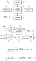
- FIG. 1 is a block diagram of a data processing system 20 according to the present invention.
- the data processing system 20 includes data processing circuitry 21, and peripheral devices 23, 25, 27 and 29.
- the data processing circuitry 21 is connected to each of the peripheral circuitries 23, 25, 27 and 29 for transfer of information between data processing circuitry 21 and peripheral circuities 23, 25, 27 and 29.
- a data processing system according to the present invention could include any quantity and type of peripheral circuitries and peripheral devices (such as peripherals 23, 25, 27 and 29) interconnected among themselves and with data processing circuitry 21 in any manner heretofore or hereafter conceivable to workers in the art.
- Examples are: data processing circuitry 21, a microprocessor; peripheral 23, a memory control unit for accessing a DRAM; peripheral 25, a bus control unit; peripheral 27, a non-volatile memory such as ROM or EPROM; and peripheral 29, a graphics control unit for interfacing with a graphics display unit.
- Other examples are: data processing circuitry 21, an adder circuit module; peripheral 23, an on-chip cache; peripheral 25, an execution/load-store unit; and peripheral 27, a branch offset,
- FIG. 2 illustrates in more detail a portion of the data processing circuitry 21 of Figure 1.
- Data processing logic at 31 receives inputs at 33 and performs data processing operations in response thereto to provide outputs at 35 which are input to the next block of data processing logic 47.
- the inputs 33 are driven by the outputs of latching circuitry 37.
- the inputs of latching circuitry 37 are connected to the data to be processed by data processing logic 31.
- the load signal clocks the latches of latching circuitry 37 so that the desired data is provided at the inputs 33 of data processing logic 31. Once the desired data has been latched through latching circuitry 37 to the inputs 33 of data processing logic 31, then data processing logic 31 provides outputs at 35 in response to the inputs at 33.
- Data processing logic 31 requires an amount of time, referred to herein as processing time, before the outputs 35 are provided in response to the inputs 33. Thus, after the inputs 33 have been latched through latching circuitry 37, the outputs 35 are not available for use by the next logic block 47 until the processing time associated with logic block 31 has elapsed. Once the processing time has elapsed, then logic 31 has completed its data processing operations and the outputs at 35 are ready and available for input to the next logic block 47. Thus, although the next logic block 47 must wait until the processing time has elapsed before beginning its data processing operations, it is desirable from a performance standpoint to enable logic block 47 to begin its data processing operations as soon as the outputs 35 from logic 31 are available and ready.
- a transition detector embodied by latch circuit 41 in Figure 2, and circuitry for implementing a self-timed function 43 are provided.
- the transition detector 41 is a single latch circuit, for example a D type flip-flop, having its data input connected to logic 1 and having its clock input connected to the load signal.
- the latch circuit 41 also clocks logic 1 through to its data output in response to the load signal.
- the data output of latch circuit 41 thus serves as a transition detection signal 39 which is input to the self-timed circuitry 43.
- the self-timed function at 43 is designed to account for the processing time associated with data processing logic 31.
- the self-timed function 43 upon receiving the transition detection signal 39 from the transition detector latch 41, the self-timed function 43 thereafter outputs a done signal when the processing time has elapsed.
- the next block of data processing logic 47 receives the done signal and responds thereto by beginning its data processing operation on the outputs 35 provided by data processing logic 31, which outputs 35 are now ready and available for processing by data processing logic 47.
- the data processing logic 47 can begin its data processing operation as soon as possible after the outputs 35 are available and ready (that is, after the processing time of data processing logic 31 has elapsed).
- the done signal is also fed back to the reset input of transition detector latch 41 so that the transition detection signal 39 goes low again when the done signal goes high.
- Only a single latch circuit 41 for example a single register bit or a single flip-flop, is required to produce the transition detection signal 39, regardless of the size of data processing logic 31 or the number of inputs thereto at 33. This is advantageous both from a power consumption standpoint and an integrated circuit area standpoint.
- Figure 3 illustrates one example of the self-timed function 43 of Figure 2.
- the self-timed function is implemented with bit-slice logic which is literally a duplicate of the worst case path, timewise, through the data processing logic circuitry 31.
- bit-slice logic which is literally a duplicate of the worst case path, timewise, through the data processing logic circuitry 31.
- the worst case path would be the path of the most significant bit of either 32-bit input.
- the logic of the path of the most significant input bit is literally duplicated in the bit-slice logic of the Figure 3 self-timed function.
- Figure 4 illustrates another example of the self-timed function 43 of Figure 2.
- a chain of inverters is arranged so as to mimic the processing delay time of the bit-slice logic of Figure 3.
- inverters are illustrated in Figure 4, a chain of other suitable delay elements will also suffice.
- the self-timed function of Figure 4 will generally approximate the processing time of data processing logic 31 less accurately than the bit-slice logic of Figure 3, but the arrangement of Figure 4 is typically less costly in terms of power consumption and integrated circuit area.
Landscapes
- Engineering & Computer Science (AREA)
- Software Systems (AREA)
- Theoretical Computer Science (AREA)
- Physics & Mathematics (AREA)
- General Engineering & Computer Science (AREA)
- General Physics & Mathematics (AREA)
- Power Sources (AREA)
- Logic Circuits (AREA)
Applications Claiming Priority (2)
| Application Number | Priority Date | Filing Date | Title |
|---|---|---|---|
| US30982594A | 1994-09-21 | 1994-09-21 | |
| US309825 | 1994-09-21 |
Publications (2)
| Publication Number | Publication Date |
|---|---|
| EP0703530A2 true EP0703530A2 (fr) | 1996-03-27 |
| EP0703530A3 EP0703530A3 (fr) | 1996-08-14 |
Family
ID=23199823
Family Applications (1)
| Application Number | Title | Priority Date | Filing Date |
|---|---|---|---|
| EP95114544A Withdrawn EP0703530A3 (fr) | 1994-09-21 | 1995-09-15 | Détection de transitions logiques dans un système de traitement de données |
Country Status (3)
| Country | Link |
|---|---|
| US (1) | US5698996A (fr) |
| EP (1) | EP0703530A3 (fr) |
| JP (1) | JPH0916280A (fr) |
Cited By (2)
| Publication number | Priority date | Publication date | Assignee | Title |
|---|---|---|---|---|
| EP0833451A3 (fr) * | 1996-09-27 | 1999-10-20 | Siemens Aktiengesellschaft | Circuit comportant des blocs combinatoires avec registres intermédiaires |
| DE102011108576A1 (de) * | 2011-07-27 | 2013-01-31 | Texas Instruments Deutschland Gmbh | Selbstgetaktete Multipliziereinheit |
Families Citing this family (4)
| Publication number | Priority date | Publication date | Assignee | Title |
|---|---|---|---|---|
| EP0880738A1 (fr) * | 1996-11-15 | 1998-12-02 | Koninklijke Philips Electronics N.V. | Circuit de traitement de donnees comportant une unite d'execution d'instructions a synchronisation automatique |
| US5912900A (en) * | 1996-12-13 | 1999-06-15 | International Business Machines Corporation | Method and system for testing self-timed circuitry |
| US5939898A (en) * | 1997-06-24 | 1999-08-17 | International Business Machines Corporation | Input isolation for self-resetting CMOS macros |
| US6522170B1 (en) * | 1998-04-27 | 2003-02-18 | International Business Machines Corporation | Self-timed CMOS static logic circuit |
Family Cites Families (10)
| Publication number | Priority date | Publication date | Assignee | Title |
|---|---|---|---|---|
| US3925652A (en) * | 1975-03-26 | 1975-12-09 | Honeywell Inf Systems | Current mode carry look-ahead array |
| US4039858A (en) * | 1976-04-05 | 1977-08-02 | Rca Corporation | Transition detector |
| JPS62151053A (ja) * | 1985-12-25 | 1987-07-06 | Iwatsu Electric Co Ltd | ノイズ除去回路 |
| US4692635A (en) * | 1986-06-26 | 1987-09-08 | National Semiconductor Corp. | Self-timed logic level transition detector |
| US4940904A (en) * | 1988-05-23 | 1990-07-10 | Industrial Technology Research Institute | Output circuit for producing positive and negative pulses at a single output terminal |
| US5121003A (en) * | 1990-10-10 | 1992-06-09 | Hal Computer Systems, Inc. | Zero overhead self-timed iterative logic |
| US5124584A (en) * | 1990-10-22 | 1992-06-23 | Sgs-Thomson Microelectronics, Inc. | Address buffer circuit with transition-based latching |
| US5566129A (en) * | 1992-02-28 | 1996-10-15 | Sony Corporation | Semiconductor memory device with address transition detector |
| US5194768A (en) * | 1992-03-27 | 1993-03-16 | Advanced Micro Devices, Inc. | Apparatus for filtering noise from a periodic signal |
| US5475320A (en) * | 1994-08-11 | 1995-12-12 | Texas Instruments Incorporated | Data processing with a self-timed approach to spurious transitions |
-
1995
- 1995-09-15 EP EP95114544A patent/EP0703530A3/fr not_active Withdrawn
- 1995-09-21 JP JP7243402A patent/JPH0916280A/ja active Pending
-
1996
- 1996-08-01 US US08/692,795 patent/US5698996A/en not_active Expired - Lifetime
Non-Patent Citations (1)
| Title |
|---|
| None |
Cited By (3)
| Publication number | Priority date | Publication date | Assignee | Title |
|---|---|---|---|---|
| EP0833451A3 (fr) * | 1996-09-27 | 1999-10-20 | Siemens Aktiengesellschaft | Circuit comportant des blocs combinatoires avec registres intermédiaires |
| DE102011108576A1 (de) * | 2011-07-27 | 2013-01-31 | Texas Instruments Deutschland Gmbh | Selbstgetaktete Multipliziereinheit |
| US9047140B2 (en) | 2011-07-27 | 2015-06-02 | Texas Instruments Incorporated | Independently timed multiplier |
Also Published As
| Publication number | Publication date |
|---|---|
| US5698996A (en) | 1997-12-16 |
| EP0703530A3 (fr) | 1996-08-14 |
| JPH0916280A (ja) | 1997-01-17 |
Similar Documents
| Publication | Publication Date | Title |
|---|---|---|
| US4841440A (en) | Control processor for controlling a peripheral unit | |
| US7062666B2 (en) | Signal-initiated method for suspending operation of a pipelined data processor | |
| US5630143A (en) | Microprocessor with externally controllable power management | |
| US4144562A (en) | System and method for increasing microprocessor output data rate | |
| EP0579369A1 (fr) | Unité centrale de traitement ayant une consommation réduite | |
| US5632037A (en) | Microprocessor having power management circuitry with coprocessor support | |
| TW338817B (en) | Computer system with touchpad support in operating system | |
| US20050114723A1 (en) | Interruption control system and method | |
| JPH076151A (ja) | オンチップメモリデバイスのアクセスのために最適化されたcpuコアバス | |
| US5881271A (en) | System and method for clock management | |
| US5983339A (en) | Power down system and method for pipelined logic functions | |
| US5708816A (en) | Method and apparatus for interrupt management for low power PDA | |
| US5163145A (en) | Circuit for determining between a first or second type CPU at reset by examining upper M bits of initial memory reference | |
| US5475320A (en) | Data processing with a self-timed approach to spurious transitions | |
| US5698996A (en) | Data processing with self-timed feature and low power transition detection | |
| EP1233325A2 (fr) | Appareil terminal et méthode de commande d'horloge en temps réel | |
| CN217932650U (zh) | 上电控制模块及机箱 | |
| US7363408B2 (en) | Interruption control system and method | |
| EP1237066B1 (fr) | Microprocesseur avec gestion d'alimentation commandée par hardware et broches de commande d'entrée/sortie pouvant être sélectionnées et méthode correspondante | |
| WO1986000734A1 (fr) | Transfert de donnees a haute vitesse entre un premier et un deuxieme organes de traitement | |
| US5742842A (en) | Data processing apparatus for executing a vector operation under control of a master processor | |
| CN100410911C (zh) | 中断控制器、中断信号预处理电路及其中断控制方法 | |
| EP0855639A1 (fr) | Registres de synchronisation à gâchette controllée pour circuits de basse puissance | |
| US20050086407A1 (en) | Interruption control system and method | |
| US6092132A (en) | Method and apparatus for monitoring 60x bus signals at a reduced frequency |
Legal Events
| Date | Code | Title | Description |
|---|---|---|---|
| PUAI | Public reference made under article 153(3) epc to a published international application that has entered the european phase |
Free format text: ORIGINAL CODE: 0009012 |
|
| AK | Designated contracting states |
Kind code of ref document: A2 Designated state(s): DE FR GB IT NL |
|
| PUAL | Search report despatched |
Free format text: ORIGINAL CODE: 0009013 |
|
| AK | Designated contracting states |
Kind code of ref document: A3 Designated state(s): DE FR GB IT NL |
|
| 17P | Request for examination filed |
Effective date: 19970129 |
|
| 17Q | First examination report despatched |
Effective date: 19990722 |
|
| STAA | Information on the status of an ep patent application or granted ep patent |
Free format text: STATUS: THE APPLICATION IS DEEMED TO BE WITHDRAWN |
|
| 18D | Application deemed to be withdrawn |
Effective date: 20000203 |