EP0703086A2 - Method and apparatus for printing having logic circuitry to reduce video data input rate - Google Patents
Method and apparatus for printing having logic circuitry to reduce video data input rate Download PDFInfo
- Publication number
- EP0703086A2 EP0703086A2 EP95306785A EP95306785A EP0703086A2 EP 0703086 A2 EP0703086 A2 EP 0703086A2 EP 95306785 A EP95306785 A EP 95306785A EP 95306785 A EP95306785 A EP 95306785A EP 0703086 A2 EP0703086 A2 EP 0703086A2
- Authority
- EP
- European Patent Office
- Prior art keywords
- bits
- printhead
- printing
- image data
- printing apparatus
- Prior art date
- Legal status (The legal status is an assumption and is not a legal conclusion. Google has not performed a legal analysis and makes no representation as to the accuracy of the status listed.)
- Granted
Links
Images


Classifications
-
- G—PHYSICS
- G06—COMPUTING; CALCULATING OR COUNTING
- G06K—GRAPHICAL DATA READING; PRESENTATION OF DATA; RECORD CARRIERS; HANDLING RECORD CARRIERS
- G06K15/00—Arrangements for producing a permanent visual presentation of the output data, e.g. computer output printers
- G06K15/02—Arrangements for producing a permanent visual presentation of the output data, e.g. computer output printers using printers
- G06K15/10—Arrangements for producing a permanent visual presentation of the output data, e.g. computer output printers using printers by matrix printers
- G06K15/102—Arrangements for producing a permanent visual presentation of the output data, e.g. computer output printers using printers by matrix printers using ink jet print heads
- G06K15/105—Multipass or interlaced printing
- G06K15/107—Mask selection
-
- B—PERFORMING OPERATIONS; TRANSPORTING
- B41—PRINTING; LINING MACHINES; TYPEWRITERS; STAMPS
- B41J—TYPEWRITERS; SELECTIVE PRINTING MECHANISMS, i.e. MECHANISMS PRINTING OTHERWISE THAN FROM A FORME; CORRECTION OF TYPOGRAPHICAL ERRORS
- B41J2/00—Typewriters or selective printing mechanisms characterised by the printing or marking process for which they are designed
- B41J2/005—Typewriters or selective printing mechanisms characterised by the printing or marking process for which they are designed characterised by bringing liquid or particles selectively into contact with a printing material
- B41J2/01—Ink jet
- B41J2/205—Ink jet for printing a discrete number of tones
-
- G—PHYSICS
- G06—COMPUTING; CALCULATING OR COUNTING
- G06K—GRAPHICAL DATA READING; PRESENTATION OF DATA; RECORD CARRIERS; HANDLING RECORD CARRIERS
- G06K2215/00—Arrangements for producing a permanent visual presentation of the output data
- G06K2215/0002—Handling the output data
- G06K2215/0062—Handling the output data combining generic and host data, e.g. filling a raster
- G06K2215/0071—Post-treatment of the composed image, e.g. compression, rotation
- G06K2215/0074—Depleting the image
Definitions
- This invention relates generally to a liquid ink printing apparatus and more particularly to a method and apparatus for reducing the data rate to liquid ink jet print elements when printing in a checkerboard or gray tone mode.
- ink jet printers print most effectively when the spots of liquid ink are deposited on a recording medium, such as paper or a transparency, in a manner which prevents the flow of liquid ink from one spot of liquid ink to an adjacent spot of liquid ink.
- a recording medium such as paper or a transparency
- ink jet printers print a line or a swath of information in at least two passes of the printhead, one overlapping the other.
- a first pass by the printhead prints diagonally adjacent pixel areas in each of two adjacent lines of pixels, so that there is no overlap of ink spots from adjacent pixel areas when the ink is still in a flowable state.
- a second pass deposits ink droplets in the remaining diagonally adjacent pixel areas in either a reverse or a same direction.
- This type of printing is typically called checkerboard printing and is enabled by firing the odd numbered jets in the odd numbered vertical columns of pixels, also referred to as strokes, and the even numbered jets in the even numbered vertical strokes during one of the passes.
- the complementary jets are fired i.e. even numbered jets within the odd number vertical strokes and the odd numbered jets within the even numbered vertical strokes. After two passes of the printhead, 100% coverage of the printed swath is achieved.
- the first pass of liquid ink droplets dries for a period of time before the second pass of liquid ink droplets is deposited.
- certain advantages are achieved, which include, enhancing the optical density of printing, reducing intercolor bleed, and reducing the cockle and curl of the paper due to the deposition of liquid ink droplets.
- US-A-4,748,453 describes a method of depositing spots of liquid ink on a substrate to prevent the flow of liquid ink from one spot which overlaps an adjacent spot.
- a first checkerboard pattern having only diagonally adjacent pixel areas is deposited in a first pass.
- the complementary checkerboard pattern is deposited. Ink is not deposited on horizontally and vertically adjacent pixel areas during the single passes, since the spots on these adjacent areas have overlapping portions.
- US-A-5,233,366 describes half-tone printing with a thermal ink jet printer using random spot distribution in one dimension.
- the individual ink ejectors of the printhead for the ink jet printer are operated according to a probability function which controls the frequency of a random activation of the ejectors as the print medium or sheet moves past the ejectors.
- checkerboard printing improves the quality of the final printed image
- checkerboard printing suffers from the fact that instead of taking one pass to print a swath of information, now two passes or more, of the carriage are required to print the same swath of information.
- marking speed which is limited by the amount of time it takes to eject ink from a nozzle.
- traversal speed or carriage pass speed of each pass there is, however, a need to double the traversal speed or carriage pass speed of each pass to equal the throughput of a single pass approach.
- resolutions and prints speeds however, increase, the data rate to the printhead becomes high which could adversely impact printhead operation and printer apparatus design.
- a 21.6cm ( 8.5'') X 27.9cm (11''), 300 X 300 dot per 2.54cm (inch), 4 page per minute printer requires data rates of about 561 kilobits per second.
- a 21.6cm ( 8.5'') X 27.9cm (11'') 600 X 600 dot per 2.54cm (inch), 8 page per minute printer requires data rates of about 4488 kilobits per second. Consequently, it is desirable to reduce the data rate to the printhead when printing in a checkerboard mode if higher print speeds are desired.
- a printing apparatus having a printhead with a plurality of nozzles for printing an image on a recording medium according to a bitmap of image data having rows and columns.
- the printing apparatus includes selecting means for selecting a portion of the bitmap of image data with the portion selected having selected bits and unselected bits and directing means, in communication with said selecting means, for directing the printhead to emit liquid ink from selected ones of the plurality of nozzles according to the selected bits.
- a further aspect of the invention is to provide a method for printing an image on a recording medium with a printhead having a plurality of nozzles according to a bitmap of image data having rows and columns.
- the method includes selecting a portion of the bitmap of image data with the portion selected having selected bits and unselected bits, transferring the selected bits only in a serial fashion and directing the printhead to emit liquid ink from selected ones of the nozzles according to the selected bits.
- An additional aspect of the invention is to provide a printing apparatus having a printhead with a plurality of drivers for causing ink to be ejected from nozzles to print an image on a recording medium according to a bitmap of image data having rows and columns.
- the printing apparatus includes an electronic selection circuit receiving a selected portion of the bitmap of image data and outputting selected bits of the selected portion, an electronic transfer circuit coupled to the electronic selection circuit receiving the selected bits of the selected portion and outputting the selected bits of the selected portion, and an electronic control circuit coupled to the electronic transfer circuit for receiving the selected bits of the selected portion and outputting the selected bits to selected drivers of the printhead.
- FIG. 8 illustrates a perspective view of an ink jet printer 9 having an ink jet printhead cartridge 10 mounted on a carriage 12 supported by carriage rails 14.
- the carriage rails 14 are supported by a frame 15 of the ink jet printer 9.
- the printhead cartridge 10 includes a housing 16 containing ink for supply to a thermal ink jet printhead 18 which selectively expels droplets of ink under control of electrical signals received from a controller (not shown) of the printer 9 through an electrical cable 20.
- the printhead 18 contains a plurality of ink channels (not shown) which carry ink from the housing 16 to respective ink ejecting orifices or nozzles (also not shown).
- the carriage 12 reciprocates or scans back and forth along the carriage rails 14 in the direction of the arrow 22.
- a recording medium 24 such as a sheet of paper or a transparency
- droplets of ink are expelled from selected ones of the printhead nozzles towards the sheet of paper.
- the ink ejecting orifices or nozzles are typically arranged in a linear array perpendicular to the scanning direction 22.
- the recording medium 24 is held in a stationary position. At the end of each pass, however, the recording medium is stepped in the direction of the arrow 26.
- a swath of information having a height which is equal to the height of the linear array of nozzles is printed while the recording medium 24 is held stationary. Once the swath of information is printed, the recording medium 24 is stepped a distance equal to a height of the linear array of nozzles so that a second adjacent swath of information can be printed.
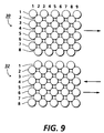
- Single pass printing can lead to various print problems. To overcome these problems, a swath of information can be printed in a first pass of information 30 and a second pass of information 32 as illustrated in FIG. 9.
- Each pass consists of a checkerboard pattern in which dots are alternately printed in both the horizontal and vertical directions so that spaces remain between dots deposited in a column and dots deposited in a row.
- the first pass 30, as illustrated consists of nine columns and eight rows of dots, however, the number of columns and rows may be varied as desired.
- the first pass 30 is printed by firing only the odd numbered jets in the odd numbered strokes here shown as vertical columns 1, 3, 5, and 7 and firing the even numbered jets in the even numbered jets in the even numbered strokes or columns 2, 4, 6 and 8.
- the complementary jets are fired as shown in which only the even numbered jets within the odd numbered strokes or columns 1, 3, 5, and 7 are fired and only the odd numbered jets in the even numbered strokes 2, 4, 6 and 8 are fired, thus, achieving 100% coverage of the printed swath. It is also possible to offset the second pass 32 from the first pass 30 by a number of rows so that banding is reduced or prevented.
- bitmapped imaged data received from a computer or some other source of information is received by the liquid ink printing apparatus.
- Bitmapped imaged data typically exists as a 2-dimensional array of individual bits (either is or Os) which indicate whether or not a spot of ink should be deposited at the location of the bit in the bitmap. Typically, if a bit is a 1, it indicates that a spot of ink should be deposited and if a bit is 0 it indicates that no spot of ink should be deposited in that location.
- a mask is applied to the bitmap to force selected bits of the bitmap to zero in a checkerboard fashion so that, when printed, no ink is deposited where bits are forced to zero.
- a vertical slice of the bitmapped image data which has been masked is extracted from the bitmap, the vertical slice typically having a vertical height equal to the number, N, of nozzles in the linear array of nozzles and having a width of 1-bit wide.
- Each bit of the vertical slice including the bits which were forced to white (zero) is then shipped serially to the printhead for firing each of the nozzles. Parallel shipping of data can also be used, however, serializing the data reduces interconnect and printhead wire bond counts.
- a second adjacent vertical slice of the masked bitmapped imaged data is extracted.
- this data is shipped serially to a print element for firing each of the nozzles of the printhead. Printing of each vertical slice in a swath is completed until a single pass is completed. After completion, the complementary pass is printed vertical slice by vertical slice.
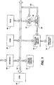
- a central processing unit or CPU 40 is connected through a bus 42 to an interface 44 which, in turn, is connected to an external device such as a host computer.
- the host computer provides information in the form of a bitmapped image to the printer for printing.
- the CPU 40 is also connected to a read only memory (ROM) 46 which includes an operating program for the CPU 40.
- ROM read only memory
- RAM random access memory
- a printer control circuits 50 are also connected to the bus 42 for operation of the printing apparatus which includes carriage driver circuits and paper feed driver circuits as is known by those skilled in the art.
- the printhead 18 (Fig.8) is also controlled by the central processing unit 40 according to the content of signals received over the bus 42 and sent to various printhead control circuits 52.
- the printhead control circuits 52 control the ejection of inks from the nozzles of a printhead element 54 contained in the printhead 18.
- a data packer circuit 56 is coupled to the bus 42.
- the data packer circuit 56 receives a vertical slice of the bitmapped imaged data which is typically stored in the RAM 48. Coupled to the data packer circuit 56 via line 68 is a data unpacker circuit 58.
- the data unpacker circuit 58 is also coupled to the printhead control circuits 52.
- a control line 60 coupled to the bus 42 receives control information from the CPU 40 and is connected to both the data packer 56 and the data unpacker 58.
- the vertical slice of bitmapped imaged data also known as video data
- the data packer 56 is removed from its temporary storage location in the RAM 48 and every other bit in the vertical slice of bitmapped imaged data is removed by the data packer 56.
- This bitmap has not had a mask applied to it. This reduces the bit count by one-half if the vertical slice of bitmapped imaged data contains an even number of bits. Every other bit is removed by an electronic selection circuit 64 of the data packer 56, one embodiment of which is illustrated in FIG. 2.
- the vertical slice of bitmapped information contained in a slice buffer 62 typically residing in the RAM 48 stores eight bits of information from a single bit wide column of information retrieved from the bitmap.
- the eight bits of bitmapped information are passed to a bit selector 64 which selects certain bits contained in the slice buffer 62 according to a signal carried by the control line 60.
- the signal carried by the control line 60 causes the bit selector 64 to select every other bit contained in the slice buffer when printing in a checkerboard pattern as previously described. Consequently, the bit selector 64 includes four output lines since one-half of the information contained in the slice buffer 62 has now been deleted.
- This parallel information contained on the output lines of the bit selector 64 is sent to a parallel to serial logic circuit 66 which converts the parallel output of the bit selector 64 to serial information which is transferred over a serial information line 68.
- a parallel to serial logic circuit 66 which converts the parallel output of the bit selector 64 to serial information which is transferred over a serial information line 68.
- Each of these circuit elements illustrated in FIG. 2 is also coupled to timing lines (not shown) for controlling the timing of the circuitry as is understood by those skilled in the art.
- the print element 54 scans across the recording medium, adjacent vertical slices of data are manipulated and printed alternating between odd and even nozzles.
- the first vertical slice of information in column 1 stored in the slice buffer 62 would contain the bits 1 through 8. Since only the odd bits are to be selected (bits 1, 3, 5, and 7), the logic control line 60 passes, for example, a zero to the bit selector 64 thereby requiring that only the odd bits are selected and transferred to the parallel serial logic circuit 66. This information is then sent to the data unpacker 58 over the line 68 (FIG. 1). After transmission of the first slice, a second slice of vertical information, here shown as the information in column 2, is selected.
- the control line 60 then carries a signal of a one (or high), for example, requiring that only the even bits 2, 4, 6 and 8 are selected by the bit selector 64 and sent through the parallel-to-serial logic circuit 66 and over the line 68 to the data unpacker 58.
- the present invention transfers one-half the pixel information available in the slice buffer 62. By transferring one-half of the pixel information, the data clocking rate is reduced by one-half.
- the bit selector 64 may be, for example, a two line to one line N bit wide data selector/multiplexer logic circuit 70 in which N is the number of bits to be selected from the slice buffer 62.
- N is the number of bits to be selected from the slice buffer 62.
- One embodiment of such selector circuit 70 is illustrated in FIG. 3.
- the control line 60 is coupled to a first AND gate 72 through an inverter 74.
- the control line 60 is also coupled to a second AND gate 76.
- the first AND gate 72 also receives the first or topmost bit of information contained in the slice buffer 62 from a line 78 corresponding to the line 78 of FIG. 2.
- the second AND gate 76 receives a second bit in the column of bits stored in the slice buffer 62 along a line 80 corresponding to the line 80, also shown in FIG. 2.
- a NOR gate 82 receives the output of the first AND gate 72 and the second AND gate 76 to generate an output on a line 84 which corresponds to the line 84 of FIG. 2 and which carries one of the selected bits from the first of two bits held in the slice buffer 62.
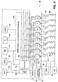
- FIG. 4 is a schematic diagram illustrating the basic elements of a printhead integrated circuit used to selectively expel ink from the array of linearly aligned nozzles.
- a thermal ink jet integrated circuit or chip 86 includes 192 thermal ink jet heating elements 88 which are powered by a 40 volt power supply 90 available from the printer 9 (FIG. 8).
- a voltage regulator 92 regulates power received from the 40 volt power supply 90.
- Each of the heating elements 88 is additionally coupled to a power MOS FET driver 94 having one side thereof coupled to a ground 96.
- the power MOS FET drivers 94 energize the heating elements 88 for expelling ink from the nozzles.
- the present invention is applicable to any number of ink jet heating elements 88, however, eight heating elements 88 are shown in FIG. 4 for illustrative purposes.
- each of the power MOS FET drivers 94 is accomplished by an AND gate 100 having the output thereof coupled to the gate of the driver 94.
- the voltage regulator 92 provides an output of greater than five volts and typically of 13 volts for supply to the AND gates 100. This operating voltage for the AND gates 100 enables the power MOS FET drivers 94 to be turned on harder through the application of a higher gate voltage than would be available from five volt power supply 102 also available from the printer 9. (FIG. 8)
- the thermal ink jet integrated circuit 86 controls up to eight heaters 88 at a time by using a bi-directional X-bit pointer shift register 104. Using this configuration, segments of the linear array of nozzles are sequentially fired, as described in US-A-5,300,968. The length of the shift register 104 depends on the number of heaters 88 fired together and the total number of heaters 88 in the printhead itself. Since the present invention is being described with reference to a 192 nozzle ink-jet printhead, X is equal to 24 since eight heaters are controlled at a time.
- Printing is initiated with a single one bit pointer which begins at the left most side of the shift register 104 at a line or conductor 106.
- the pointer bit starts at the left-hand side and propagates to the right-hand side or, in the alternative starts on the right-hand side and propagates to the left-hand side depending on the state of the data line 68 at the time a reset line 105 goes high. Bi-directional propagation of the single bit is necessary for bi-directional printing.
- the shift register 104 is reset by the reset line 105
- four bits of data received from the data line 68 are loaded into a four bit shift register 108.
- the four-bit shift register 108 is shifted by a shift line 109 which receives shift information from the CPU 40 as understood by one skilled in the art.
- the four bits of data which are then loaded into a four bit latch circuit 110, control whether or not an odd or even heating elements 88 corresponding to odd or even numbered AND gates 100 within a block of eight heating elements will be energized.
- a fire control pulse received from the printhead CPU 40 at a fire line 112 controls the amount of time that individual heaters 88 are energized.
- four new bits of information are loaded into the four bit shift register 108.
- the completion of the fire cycle advances the shift register 104 pointer bit one position and the fire cycle begins again.
- the latch 110 is used to latch the information from the four-bit shift register 108 onto the individual MOS FET drivers 94 for energization.
- each of the heaters 88 for printing a checkerboard pattern is accomplished by an enable signal received over the control line 60 which selects either an odd or an even numbered AND gate 100.
- the combination of the enable signal 60 and the three-input AND gates 100 comprise the data unpacker 58 for selectively addressing either the odd or the even heaters 88.
- every pair of odd and even AND gates are coupled to the same output line of the latch 110 so that the data is available at an odd and even AND gate.
- the enabling signal received over the control line or enabler 60 is coupled to the odd numbered AND gates 100 through an inverter 114.
- the even numbered AND gates are coupled to the control line 60 directly.
- the enabling signal is a 0
- the AND gates 1, 3, 5, and 7 receive a 1 at the input so that the data available at the input to the AND gates from the latch 110 fires the appropriate heaters 88.
- the control line 60 includes an enabling signal of a 1, the inputs at the even numbered AND gates are enabled so that these individual AND gates control their respective heaters 88. In this fashion, odd numbered heaters only or even numbered heaters only are selectively activated for checkerboard printing.
- FIG. 5 illustrates a second embodiment of the integrated circuit chip 86 incorporating the present invention.
- data is sent over the data line 68 to the four-bit shift register 108 as previously described.
- the output of the four-bit shift register 108 is instead coupled to a slice reconstruction circuit 116 which inserts the data removed by the data packer 56 and applied to the data line 68.
- the slice reconstruction circuit is coupled to the enable line 60 which controls whether the four bits output from the four-bit shift register 108 will be directed to odd or even and gates 100. If, for instance, the enable signal is a 0 it indicates that the four bits received from the four-bit shift register 108 will be directed to the odd numbered AND gates.
- the even and gates 2, 4, 6 and 8 should not fire a respective heater 88 and a 0 is inserted between each of the odd numbered bits by the slice reconstruction circuit 116. If, on the other hand, the enable signal is a 1, indicating that the four bits at the output of the four-bit shift register are to be directed to the even numbered AND gates 100, then the slice reconstruction circuit 116 will insert a 0 on the odd numbered output lines.
- a portion of the bit slice reconstruction circuit 116 is illustrated in FIG. 6 for directing a single input bit received from the four-bit shift register 108 to one of two output lines of the circuit 116.
- the top most bit of the four bit shift register 108 is input to a first line 118 of the slice reconstruction circuit 116.
- the enable line 60 is also coupled to the slice reconstruction circuit 116.
- a first AND gate 120 receives the input bit over the line 118 and the inverse of the enable signal over the line 60.
- a second AND gate 122 receives the first bit over the line 118 and the signal of the enable line 60.
- the first bit received from the four-bit shift register on the line 118 will be directed to either the output of the first AND gate 120 or the output of the second AND gate 122 having output lines 124 and 126 respectively.
- one of the output lines 124 or 126 is driven according to the bit received from the four-bit shift register while the other line is set to a 0 so that the appropriate odd or even AND gates 100 is not fired.
- the present invention reduces data rates by one-half for printing of checkerboard patterns in which every other bit in a column and every other bit in a row is not printed in a single pass.
- the present invention is also equally applicable to printing in which every third bit is printed in a single pass. Such printing, however, requires three passes of the printhead for full coverage.
- two control lines as opposed to one would be required. The benefit here is that of reducing the data rate by two-thirds.
- FIG. 7 illustrates a possible implementation of the control lines. As seen in FIG. 7, every third bit is printed in a single column and the printed bits are changed for different columns in a print pass.
- an odd/even stroke control for reduced data clocking rate in a liquid ink printing apparatus is provided.
- the present invention is not limited to printheads which sequentially print segments of the printhead elements as described, but can also be effectively used with printheads which print all the nozzles of the printhead at once.
- the present invention is not limited to scanning printheads, but is equally applicable to printers incorporating pagewidth printbars.
Abstract
Description
- This invention relates generally to a liquid ink printing apparatus and more particularly to a method and apparatus for reducing the data rate to liquid ink jet print elements when printing in a checkerboard or gray tone mode.
- In current drop-on-demand ink jet printers, it has been found that such printers print most effectively when the spots of liquid ink are deposited on a recording medium, such as paper or a transparency, in a manner which prevents the flow of liquid ink from one spot of liquid ink to an adjacent spot of liquid ink. To prevent the flow of liquid ink from one spot to another, ink jet printers print a line or a swath of information in at least two passes of the printhead, one overlapping the other. When printing a swath of information, a first pass by the printhead prints diagonally adjacent pixel areas in each of two adjacent lines of pixels, so that there is no overlap of ink spots from adjacent pixel areas when the ink is still in a flowable state. A second pass deposits ink droplets in the remaining diagonally adjacent pixel areas in either a reverse or a same direction. This type of printing is typically called checkerboard printing and is enabled by firing the odd numbered jets in the odd numbered vertical columns of pixels, also referred to as strokes, and the even numbered jets in the even numbered vertical strokes during one of the passes. During the second pass over the same swath, the complementary jets are fired i.e. even numbered jets within the odd number vertical strokes and the odd numbered jets within the even numbered vertical strokes. After two passes of the printhead, 100% coverage of the printed swath is achieved. By printing checkerboard patterns, the first pass of liquid ink droplets dries for a period of time before the second pass of liquid ink droplets is deposited. By providing a certain amount of time for drying, certain advantages are achieved, which include, enhancing the optical density of printing, reducing intercolor bleed, and reducing the cockle and curl of the paper due to the deposition of liquid ink droplets.
- US-A-4,748,453 describes a method of depositing spots of liquid ink on a substrate to prevent the flow of liquid ink from one spot which overlaps an adjacent spot. A first checkerboard pattern having only diagonally adjacent pixel areas is deposited in a first pass. In a second pass, the complementary checkerboard pattern is deposited. Ink is not deposited on horizontally and vertically adjacent pixel areas during the single passes, since the spots on these adjacent areas have overlapping portions.
- US-A-5,233,366 describes half-tone printing with a thermal ink jet printer using random spot distribution in one dimension. The individual ink ejectors of the printhead for the ink jet printer are operated according to a probability function which controls the frequency of a random activation of the ejectors as the print medium or sheet moves past the ejectors.
- While checkerboard printing improves the quality of the final printed image, checkerboard printing suffers from the fact that instead of taking one pass to print a swath of information, now two passes or more, of the carriage are required to print the same swath of information. At slow print speeds, there is little adverse impact on marking speed which is limited by the amount of time it takes to eject ink from a nozzle. There is, however, a need to double the traversal speed or carriage pass speed of each pass to equal the throughput of a single pass approach. As resolutions and prints speeds, however, increase, the data rate to the printhead becomes high which could adversely impact printhead operation and printer apparatus design. For example, a 21.6cm ( 8.5'') X 27.9cm (11''), 300 X 300 dot per 2.54cm (inch), 4 page per minute printer requires data rates of about 561 kilobits per second. A 21.6cm ( 8.5'') X 27.9cm (11'') 600 X 600 dot per 2.54cm (inch), 8 page per minute printer, however, requires data rates of about 4488 kilobits per second. Consequently, it is desirable to reduce the data rate to the printhead when printing in a checkerboard mode if higher print speeds are desired.
- In accordance with one aspect of the invention, there is provided a printing apparatus having a printhead with a plurality of nozzles for printing an image on a recording medium according to a bitmap of image data having rows and columns. The printing apparatus includes selecting means for selecting a portion of the bitmap of image data with the portion selected having selected bits and unselected bits and directing means, in communication with said selecting means, for directing the printhead to emit liquid ink from selected ones of the plurality of nozzles according to the selected bits.
- A further aspect of the invention is to provide a method for printing an image on a recording medium with a printhead having a plurality of nozzles according to a bitmap of image data having rows and columns. The method includes selecting a portion of the bitmap of image data with the portion selected having selected bits and unselected bits, transferring the selected bits only in a serial fashion and directing the printhead to emit liquid ink from selected ones of the nozzles according to the selected bits.
- An additional aspect of the invention is to provide a printing apparatus having a printhead with a plurality of drivers for causing ink to be ejected from nozzles to print an image on a recording medium according to a bitmap of image data having rows and columns. The printing apparatus includes an electronic selection circuit receiving a selected portion of the bitmap of image data and outputting selected bits of the selected portion, an electronic transfer circuit coupled to the electronic selection circuit receiving the selected bits of the selected portion and outputting the selected bits of the selected portion, and an electronic control circuit coupled to the electronic transfer circuit for receiving the selected bits of the selected portion and outputting the selected bits to selected drivers of the printhead.
- The present invention will now be described by way of example with reference to the accompanying drawings, in which:
- Figure 1 is a block diagram of an electronic circuit for an ink jet printer incorporating odd/even stroke control for reduced video data clocking;
- Figure 2 is block diagram of an electronic selection circuit of a data packer circuit;
- Figure 3 is a circuit diagram of a selector circuit for use in the electronic selection circuit;
- Figure 4 is a circuit diagram illustrating one embodiment of an ink jet integrated circuit;
- Figure 5 is a circuit diagram illustrating another embodiment of an ink jet integrated circuit;
- Figure 6 is a circuit diagram of a portion of a bit slice reconstruction circuit;
- Figure 7 is a functional description of control lines for use in the present invention if printing a checkerboard pattern in which three passes of a printhead are necessary to print a single swath of information;
- Figure 8 is a cutaway view of a printer utilizing thermal ink jet printheads attached to a reciprocating carriage; and
- Figure 9 is an enlarged schematic illustration of two passes of checkerboard printing.
- FIG. 8 illustrates a perspective view of an
ink jet printer 9 having an inkjet printhead cartridge 10 mounted on acarriage 12 supported bycarriage rails 14. Thecarriage rails 14 are supported by aframe 15 of theink jet printer 9. Theprinthead cartridge 10 includes ahousing 16 containing ink for supply to a thermalink jet printhead 18 which selectively expels droplets of ink under control of electrical signals received from a controller (not shown) of theprinter 9 through anelectrical cable 20. Theprinthead 18 contains a plurality of ink channels (not shown) which carry ink from thehousing 16 to respective ink ejecting orifices or nozzles (also not shown). When printing, thecarriage 12 reciprocates or scans back and forth along thecarriage rails 14 in the direction of thearrow 22. As theprinthead cartridge 10 reciprocates back and forth across arecording medium 24, such as a sheet of paper or a transparency, droplets of ink are expelled from selected ones of the printhead nozzles towards the sheet of paper. The ink ejecting orifices or nozzles are typically arranged in a linear array perpendicular to thescanning direction 22. During each pass of thecarriage 12, therecording medium 24 is held in a stationary position. At the end of each pass, however, the recording medium is stepped in the direction of thearrow 26. - In single pass printing, a swath of information having a height which is equal to the height of the linear array of nozzles is printed while the
recording medium 24 is held stationary. Once the swath of information is printed, therecording medium 24 is stepped a distance equal to a height of the linear array of nozzles so that a second adjacent swath of information can be printed. Single pass printing, however, can lead to various print problems. To overcome these problems, a swath of information can be printed in a first pass ofinformation 30 and a second pass ofinformation 32 as illustrated in FIG. 9. Each pass consists of a checkerboard pattern in which dots are alternately printed in both the horizontal and vertical directions so that spaces remain between dots deposited in a column and dots deposited in a row. For instance, as shown in FIG. 9, thefirst pass 30, as illustrated, consists of nine columns and eight rows of dots, however, the number of columns and rows may be varied as desired. Thefirst pass 30 is printed by firing only the odd numbered jets in the odd numbered strokes here shown asvertical columns columns second pass 32, the complementary jets are fired as shown in which only the even numbered jets within the odd numbered strokes orcolumns strokes second pass 32 from thefirst pass 30 by a number of rows so that banding is reduced or prevented. - In known checkerboard printing, bitmapped imaged data received from a computer or some other source of information is received by the liquid ink printing apparatus. Bitmapped imaged data typically exists as a 2-dimensional array of individual bits (either is or Os) which indicate whether or not a spot of ink should be deposited at the location of the bit in the bitmap. Typically, if a bit is a 1, it indicates that a spot of ink should be deposited and if a bit is 0 it indicates that no spot of ink should be deposited in that location.
- A mask is applied to the bitmap to force selected bits of the bitmap to zero in a checkerboard fashion so that, when printed, no ink is deposited where bits are forced to zero. A vertical slice of the bitmapped image data which has been masked is extracted from the bitmap, the vertical slice typically having a vertical height equal to the number, N, of nozzles in the linear array of nozzles and having a width of 1-bit wide. Each bit of the vertical slice including the bits which were forced to white (zero) is then shipped serially to the printhead for firing each of the nozzles. Parallel shipping of data can also be used, however, serializing the data reduces interconnect and printhead wire bond counts. At the next horizontal bit location, a second adjacent vertical slice of the masked bitmapped imaged data is extracted. Again, this data is shipped serially to a print element for firing each of the nozzles of the printhead. Printing of each vertical slice in a swath is completed until a single pass is completed. After completion, the complementary pass is printed vertical slice by vertical slice.
- It is also possible to extract a horizontal slice of the bitmapped image data, for instance, when printing with a pagewidth printbar having a linear array of nozzles aligned perpendicularly to the stepping direction of the recording medium.
- Referring to FIG. 1, there is shown a control system for an ink jet printer incorporating the present invention. A central processing unit or
CPU 40 is connected through abus 42 to aninterface 44 which, in turn, is connected to an external device such as a host computer. The host computer provides information in the form of a bitmapped image to the printer for printing. TheCPU 40 is also connected to a read only memory (ROM) 46 which includes an operating program for theCPU 40. A random access memory (RAM) 48 connected to thebus 42 includes accessible memory including print buffers for the manipulation of data and for the storage of printing information in the form of bitmaps received from the host computer. In addition to theROM 46 and theRAM 48, variousprinter control circuits 50 are also connected to thebus 42 for operation of the printing apparatus which includes carriage driver circuits and paper feed driver circuits as is known by those skilled in the art. - The printhead 18 (Fig.8) is also controlled by the
central processing unit 40 according to the content of signals received over thebus 42 and sent to variousprinthead control circuits 52. Theprinthead control circuits 52 control the ejection of inks from the nozzles of aprinthead element 54 contained in theprinthead 18. - In addition to the
printhead control circuits 52, adata packer circuit 56 is coupled to thebus 42. Thedata packer circuit 56 receives a vertical slice of the bitmapped imaged data which is typically stored in theRAM 48. Coupled to thedata packer circuit 56 vialine 68 is adata unpacker circuit 58. The data unpackercircuit 58 is also coupled to theprinthead control circuits 52. Acontrol line 60 coupled to thebus 42 receives control information from theCPU 40 and is connected to both thedata packer 56 and thedata unpacker 58. - In the present invention, the vertical slice of bitmapped imaged data, also known as video data, is removed from its temporary storage location in the
RAM 48 and every other bit in the vertical slice of bitmapped imaged data is removed by thedata packer 56. This bitmap has not had a mask applied to it. This reduces the bit count by one-half if the vertical slice of bitmapped imaged data contains an even number of bits. Every other bit is removed by anelectronic selection circuit 64 of thedata packer 56, one embodiment of which is illustrated in FIG. 2. - As illustrated in FIG. 2, it is presumed for the purposes of illustration that the vertical slice of bitmapped information contained in a
slice buffer 62 typically residing in theRAM 48 stores eight bits of information from a single bit wide column of information retrieved from the bitmap. The eight bits of bitmapped information are passed to abit selector 64 which selects certain bits contained in theslice buffer 62 according to a signal carried by thecontrol line 60. The signal carried by thecontrol line 60 causes thebit selector 64 to select every other bit contained in the slice buffer when printing in a checkerboard pattern as previously described. Consequently, thebit selector 64 includes four output lines since one-half of the information contained in theslice buffer 62 has now been deleted. This parallel information contained on the output lines of thebit selector 64 is sent to a parallel toserial logic circuit 66 which converts the parallel output of thebit selector 64 to serial information which is transferred over aserial information line 68. Each of these circuit elements illustrated in FIG. 2 is also coupled to timing lines (not shown) for controlling the timing of the circuitry as is understood by those skilled in the art. - As the
print element 54 scans across the recording medium, adjacent vertical slices of data are manipulated and printed alternating between odd and even nozzles. For example, if thefirst swath 30 of FIG. 9 is printed, the first vertical slice of information incolumn 1 stored in theslice buffer 62 would contain thebits 1 through 8. Since only the odd bits are to be selected (bits logic control line 60 passes, for example, a zero to thebit selector 64 thereby requiring that only the odd bits are selected and transferred to the parallelserial logic circuit 66. This information is then sent to thedata unpacker 58 over the line 68 (FIG. 1). After transmission of the first slice, a second slice of vertical information, here shown as the information incolumn 2, is selected. Thecontrol line 60 then carries a signal of a one (or high), for example, requiring that only theeven bits bit selector 64 and sent through the parallel-to-serial logic circuit 66 and over theline 68 to thedata unpacker 58. Using this scheme, the present invention transfers one-half the pixel information available in theslice buffer 62. By transferring one-half of the pixel information, the data clocking rate is reduced by one-half. - The
bit selector 64 may be, for example, a two line to one line N bit wide data selector/multiplexer logic circuit 70 in which N is the number of bits to be selected from theslice buffer 62. One embodiment ofsuch selector circuit 70 is illustrated in FIG. 3. Thecontrol line 60 is coupled to a first ANDgate 72 through aninverter 74. Thecontrol line 60 is also coupled to a second ANDgate 76. The first ANDgate 72 also receives the first or topmost bit of information contained in theslice buffer 62 from aline 78 corresponding to theline 78 of FIG. 2. The second ANDgate 76 receives a second bit in the column of bits stored in theslice buffer 62 along aline 80 corresponding to theline 80, also shown in FIG. 2. A NORgate 82 receives the output of the first ANDgate 72 and the second ANDgate 76 to generate an output on aline 84 which corresponds to theline 84 of FIG. 2 and which carries one of the selected bits from the first of two bits held in theslice buffer 62. - FIG. 4 is a schematic diagram illustrating the basic elements of a printhead integrated circuit used to selectively expel ink from the array of linearly aligned nozzles. In one particular embodiment, a thermal ink jet integrated circuit or
chip 86 includes 192 thermal inkjet heating elements 88 which are powered by a 40volt power supply 90 available from the printer 9 (FIG. 8). Avoltage regulator 92 regulates power received from the 40volt power supply 90. Each of theheating elements 88 is additionally coupled to a powerMOS FET driver 94 having one side thereof coupled to aground 96. The powerMOS FET drivers 94 energize theheating elements 88 for expelling ink from the nozzles. The present invention is applicable to any number of inkjet heating elements 88, however, eightheating elements 88 are shown in FIG. 4 for illustrative purposes. - Selective control of each of the power
MOS FET drivers 94 is accomplished by an ANDgate 100 having the output thereof coupled to the gate of thedriver 94. Thevoltage regulator 92 provides an output of greater than five volts and typically of 13 volts for supply to the ANDgates 100. This operating voltage for the ANDgates 100 enables the powerMOS FET drivers 94 to be turned on harder through the application of a higher gate voltage than would be available from fivevolt power supply 102 also available from theprinter 9. (FIG. 8) - To reduce the amount of circuitry necessary to individually fire each of the
heaters 88, the thermal ink jet integratedcircuit 86 controls up to eightheaters 88 at a time by using a bi-directional X-bitpointer shift register 104. Using this configuration, segments of the linear array of nozzles are sequentially fired, as described in US-A-5,300,968. The length of theshift register 104 depends on the number ofheaters 88 fired together and the total number ofheaters 88 in the printhead itself. Since the present invention is being described with reference to a 192 nozzle ink-jet printhead, X is equal to 24 since eight heaters are controlled at a time. - Printing is initiated with a single one bit pointer which begins at the left most side of the
shift register 104 at a line orconductor 106. The pointer bit starts at the left-hand side and propagates to the right-hand side or, in the alternative starts on the right-hand side and propagates to the left-hand side depending on the state of thedata line 68 at the time areset line 105 goes high. Bi-directional propagation of the single bit is necessary for bi-directional printing. When theshift register 104 is reset by thereset line 105, four bits of data received from thedata line 68 are loaded into a fourbit shift register 108. The four-bit shift register 108 is shifted by ashift line 109 which receives shift information from theCPU 40 as understood by one skilled in the art. The four bits of data, which are then loaded into a fourbit latch circuit 110, control whether or not an odd or evenheating elements 88 corresponding to odd or even numbered ANDgates 100 within a block of eight heating elements will be energized. A fire control pulse received from theprinthead CPU 40 at afire line 112, controls the amount of time thatindividual heaters 88 are energized. During the cycle of the fire control pulse, four new bits of information are loaded into the fourbit shift register 108. The completion of the fire cycle advances theshift register 104 pointer bit one position and the fire cycle begins again. Thelatch 110 is used to latch the information from the four-bit shift register 108 onto the individualMOS FET drivers 94 for energization. - Individual energization of each of the
heaters 88 for printing a checkerboard pattern, as illustrated in FIG. 9, is accomplished by an enable signal received over thecontrol line 60 which selects either an odd or an even numbered ANDgate 100. The combination of theenable signal 60 and the three-input ANDgates 100 comprise the data unpacker 58 for selectively addressing either the odd or theeven heaters 88. - As illustrated in FIG. 4, every pair of odd and even AND gates are coupled to the same output line of the
latch 110 so that the data is available at an odd and even AND gate. The enabling signal received over the control line orenabler 60 is coupled to the odd numbered ANDgates 100 through aninverter 114. The even numbered AND gates are coupled to thecontrol line 60 directly. When the enabling signal is a 0, the ANDgates latch 110 fires theappropriate heaters 88. When thecontrol line 60 includes an enabling signal of a 1, the inputs at the even numbered AND gates are enabled so that these individual AND gates control theirrespective heaters 88. In this fashion, odd numbered heaters only or even numbered heaters only are selectively activated for checkerboard printing. - FIG. 5 illustrates a second embodiment of the
integrated circuit chip 86 incorporating the present invention. In this particular embodiment, data is sent over thedata line 68 to the four-bit shift register 108 as previously described. The output of the four-bit shift register 108, however, is instead coupled to aslice reconstruction circuit 116 which inserts the data removed by thedata packer 56 and applied to thedata line 68. The slice reconstruction circuit is coupled to the enableline 60 which controls whether the four bits output from the four-bit shift register 108 will be directed to odd or even andgates 100. If, for instance, the enable signal is a 0 it indicates that the four bits received from the four-bit shift register 108 will be directed to the odd numbered AND gates. Consequently, the even andgates respective heater 88 and a 0 is inserted between each of the odd numbered bits by theslice reconstruction circuit 116. If, on the other hand, the enable signal is a 1, indicating that the four bits at the output of the four-bit shift register are to be directed to the even numbered ANDgates 100, then theslice reconstruction circuit 116 will insert a 0 on the odd numbered output lines. - A portion of the bit
slice reconstruction circuit 116 is illustrated in FIG. 6 for directing a single input bit received from the four-bit shift register 108 to one of two output lines of thecircuit 116. For example, the top most bit of the fourbit shift register 108 is input to afirst line 118 of theslice reconstruction circuit 116. The enableline 60 is also coupled to theslice reconstruction circuit 116. A first ANDgate 120 receives the input bit over theline 118 and the inverse of the enable signal over theline 60. A second ANDgate 122 receives the first bit over theline 118 and the signal of theenable line 60. Depending on the state of the enable signal on theline 60, the first bit received from the four-bit shift register on theline 118 will be directed to either the output of the first ANDgate 120 or the output of the second ANDgate 122 havingoutput lines output lines gates 100 is not fired. - The present invention reduces data rates by one-half for printing of checkerboard patterns in which every other bit in a column and every other bit in a row is not printed in a single pass. The present invention is also equally applicable to printing in which every third bit is printed in a single pass. Such printing, however, requires three passes of the printhead for full coverage. Using the proposed approach according to the present invention, however, two control lines as opposed to one would be required. The benefit here is that of reducing the data rate by two-thirds. FIG. 7 illustrates a possible implementation of the control lines. As seen in FIG. 7, every third bit is printed in a single column and the printed bits are changed for different columns in a print pass.
- In the present invention, an odd/even stroke control for reduced data clocking rate in a liquid ink printing apparatus is provided. The present invention is not limited to printheads which sequentially print segments of the printhead elements as described, but can also be effectively used with printheads which print all the nozzles of the printhead at once. Furthermore, the present invention is not limited to scanning printheads, but is equally applicable to printers incorporating pagewidth printbars.
Claims (10)
- A printing apparatus (9) having a printhead (18) with a plurality of nozzles for printing an image on a recording medium (24) according to a bitmap of image data (30,32) having rows and columns and a logic circuit (86) to reduce the input video data rate to the printhead, the printing apparatus comprising:
selecting means (56,64) for selecting a portion of the bitmap of image data with the portion selected having selected bits and unselected bits;
directing means (58), in communication with said selecting means, for directing the printhead to emit liquid ink from selected ones of the plurality of nozzles according to the selected bits. - The printing apparatus of claim 1, further comprising transfer means (66) for transferring the selected bits from said selecting means to said directing means.
- The printing apparatus of claims 1 or 2, wherein the portion selected comprises a column of bits one bit wide and N bits high; and wherein the bits selected are each spaced apart in said column by an unselected bit.
- The printing apparatus of any of the preceding claims, further comprising a logic control line (60) coupled to said selecting means, said logic control line transmitting a signal indicating which of the bits of the portion selected are to be selected.
- The printing apparatus of any of the preceding claims, further comprising a logic control line (60) coupled to said directing means (58), said logic control line transmitting a signal indicating which of the nozzles emit ink.
- The printing apparatus of any of the preceding claims, wherein said selecting means comprises a multiplexer logic circuit (70).
- A method for printing an image on a recording medium (24) with a printhead (18) having a plurality of nozzles according to a bitmap of image data (30,32) having rows and columns, the method comprising:
selecting a portion of the bitmap of image data with the portion selected having selected bits and unselected bits;
transferring the selected bits only in a serial fashion; and
directing the printhead to emit liquid ink from selected ones of the nozzles according to the selected bits. - The method of claim 7, wherein the selected portion comprises a column of bits one bit wide and N bits high.
- The method of claims 7 or 8, further comprising the step of controlling the selection of bits by a logic control signal indicating which of the bits of the portion selected are to be selected.
- A printing apparatus (9) having a printhead (18) with a plurality of drivers (94) for causing ink to be ejected from nozzles to print an image on a recording medium (24) according to a bitmap of image data (30,32) having rows and columns, the printing apparatus comprising:
an electronic selection circuit (64) receiving a selected portion of the bitmap of image data and outputting selected bits of the selected portion;
an electronic transfer circuit (66) coupled to said electronic selection circuit, receiving the selected bits of the selected portion and outputting the selected bits of the selected portion; and
an electronic control circuit (86), coupled to said electronic transfer circuit, receiving the selected bits of the selected portion and outputting the selected bits to selected drivers of the printhead
Applications Claiming Priority (2)
| Application Number | Priority Date | Filing Date | Title |
|---|---|---|---|
| US08/312,382 US5692108A (en) | 1994-09-26 | 1994-09-26 | Odd/even stroke control for reduced video data clocking |
| US312382 | 1994-09-26 |
Publications (3)
| Publication Number | Publication Date |
|---|---|
| EP0703086A2 true EP0703086A2 (en) | 1996-03-27 |
| EP0703086A3 EP0703086A3 (en) | 1998-06-03 |
| EP0703086B1 EP0703086B1 (en) | 2002-01-23 |
Family
ID=23211194
Family Applications (1)
| Application Number | Title | Priority Date | Filing Date |
|---|---|---|---|
| EP95306785A Expired - Lifetime EP0703086B1 (en) | 1994-09-26 | 1995-09-26 | Method and apparatus for printing having logic circuitry to reduce video data input rate |
Country Status (5)
| Country | Link |
|---|---|
| US (1) | US5692108A (en) |
| EP (1) | EP0703086B1 (en) |
| JP (1) | JPH08104001A (en) |
| BR (1) | BR9504160A (en) |
| DE (1) | DE69525119T2 (en) |
Cited By (1)
| Publication number | Priority date | Publication date | Assignee | Title |
|---|---|---|---|---|
| US7083266B2 (en) | 2002-10-30 | 2006-08-01 | Lexmark International, Inc. | Micro-miniature fluid jetting device |
Families Citing this family (15)
| Publication number | Priority date | Publication date | Assignee | Title |
|---|---|---|---|---|
| JP3423478B2 (en) * | 1995-05-30 | 2003-07-07 | キヤノン株式会社 | Recording device |
| CN1083337C (en) * | 1996-03-26 | 2002-04-24 | 精工爱普生株式会社 | Printing device and its control method |
| US5870112A (en) * | 1996-06-25 | 1999-02-09 | Xerox Corporation | Dot scheduling for liquid ink printers |
| KR100217996B1 (en) * | 1996-12-23 | 1999-09-01 | 윤종용 | Compensation apparatus and method of nozzle gap of print head |
| US5999705A (en) * | 1998-04-15 | 1999-12-07 | Lexmark International, Inc. | Method of interlaced printing using an ink jet printer |
| US6161918A (en) * | 1998-11-06 | 2000-12-19 | Lexmark International, Inc. | Thermal ink jet printer |
| US6154233A (en) * | 1999-04-19 | 2000-11-28 | Lexmark International, Inc. | System and method for separating raster data for printing |
| US7289243B2 (en) | 2002-08-07 | 2007-10-30 | Lexmark International, Inc. | Apparatus and method for data compression optimized by print head architecture |
| US7722185B2 (en) * | 2005-12-05 | 2010-05-25 | Silverbrook Research Pty Ltd | Cradle for printhead cartridge having power storage interface |
| US7461922B2 (en) * | 2005-12-05 | 2008-12-09 | Silverbrook Research Pty Ltd | Printing system having power regulating printhead cartridge interface |
| US7461910B2 (en) * | 2005-12-05 | 2008-12-09 | Silverbrook Research Pty Ltd | Printing system having power storage printhead cartridge interface |
| US7465020B2 (en) * | 2005-12-05 | 2008-12-16 | Silverbrook Research Pty Ltd | Printhead cartridge interface having power storage |
| US7467853B2 (en) * | 2005-12-05 | 2008-12-23 | Silverbrook Research Pty Ltd | Cradle for printhead cartridge having power regulation interface |
| US8770718B2 (en) * | 2007-04-05 | 2014-07-08 | Marvell World Trade Ltd. | Inkjet printer having switched firing of adjacent nozzles applying common color |
| CN111923606B (en) * | 2020-06-30 | 2022-03-29 | 厦门汉印电子技术有限公司 | Printer and printing method |
Citations (3)
| Publication number | Priority date | Publication date | Assignee | Title |
|---|---|---|---|---|
| US4748453A (en) | 1987-07-21 | 1988-05-31 | Xerox Corporation | Spot deposition for liquid ink printing |
| US5233366A (en) | 1992-05-26 | 1993-08-03 | Xerox Corporation | Half-tone printing with thermal ink jet using random spot distribution in one dimension |
| US5300968A (en) | 1992-09-10 | 1994-04-05 | Xerox Corporation | Apparatus for stabilizing thermal ink jet printer spot size |
Family Cites Families (12)
| Publication number | Priority date | Publication date | Assignee | Title |
|---|---|---|---|---|
| DE3273429D1 (en) * | 1981-06-19 | 1986-10-30 | Toshiba Kk | Thermal printer |
| JPS618360A (en) * | 1984-06-22 | 1986-01-16 | Ricoh Co Ltd | Charge control inkjet printer |
| JPH0678011B2 (en) * | 1984-11-27 | 1994-10-05 | 株式会社リコー | Printer |
| JP2707259B2 (en) * | 1987-11-05 | 1998-01-28 | キヤノン株式会社 | Ink jet recording device |
| US5237344A (en) * | 1987-11-05 | 1993-08-17 | Canon Kabushiki Kaisha | Ink jet recording apparatus and method with dot thinning |
| US4965593A (en) * | 1989-07-27 | 1990-10-23 | Hewlett-Packard Company | Print quality of dot printers |
| US4967203A (en) * | 1989-09-29 | 1990-10-30 | Hewlett-Packard Company | Interlace printing process |
| DE69026599T2 (en) * | 1989-10-17 | 1996-09-12 | Nakajima All Precision Co | METHOD FOR COMPRESSING CHARACTER DATA AND METHOD FOR CHANGING THE CHARACTER |
| US5012257A (en) * | 1990-03-16 | 1991-04-30 | Hewlett-Packard Company | Ink jet color graphics printing |
| JP2861251B2 (en) * | 1990-05-12 | 1999-02-24 | ブラザー工業株式会社 | Printing device |
| US5353387A (en) * | 1990-09-10 | 1994-10-04 | Mannesmann Aktiengesellschaft | Process for reducing the quantity of ink applied to recording substrates by ink printing devices to prevent image degradation |
| US5506609A (en) * | 1993-06-30 | 1996-04-09 | Apple Computer, Inc. | Minimizing color bleed while maximizing throughput for color printing |
-
1994
- 1994-09-26 US US08/312,382 patent/US5692108A/en not_active Expired - Lifetime
-
1995
- 1995-09-18 JP JP7237969A patent/JPH08104001A/en not_active Withdrawn
- 1995-09-25 BR BR9504160A patent/BR9504160A/en not_active Application Discontinuation
- 1995-09-26 DE DE69525119T patent/DE69525119T2/en not_active Expired - Fee Related
- 1995-09-26 EP EP95306785A patent/EP0703086B1/en not_active Expired - Lifetime
Patent Citations (3)
| Publication number | Priority date | Publication date | Assignee | Title |
|---|---|---|---|---|
| US4748453A (en) | 1987-07-21 | 1988-05-31 | Xerox Corporation | Spot deposition for liquid ink printing |
| US5233366A (en) | 1992-05-26 | 1993-08-03 | Xerox Corporation | Half-tone printing with thermal ink jet using random spot distribution in one dimension |
| US5300968A (en) | 1992-09-10 | 1994-04-05 | Xerox Corporation | Apparatus for stabilizing thermal ink jet printer spot size |
Cited By (1)
| Publication number | Priority date | Publication date | Assignee | Title |
|---|---|---|---|---|
| US7083266B2 (en) | 2002-10-30 | 2006-08-01 | Lexmark International, Inc. | Micro-miniature fluid jetting device |
Also Published As
| Publication number | Publication date |
|---|---|
| BR9504160A (en) | 1996-08-06 |
| JPH08104001A (en) | 1996-04-23 |
| DE69525119D1 (en) | 2002-03-14 |
| EP0703086B1 (en) | 2002-01-23 |
| DE69525119T2 (en) | 2002-07-18 |
| EP0703086A3 (en) | 1998-06-03 |
| US5692108A (en) | 1997-11-25 |
Similar Documents
| Publication | Publication Date | Title |
|---|---|---|
| KR100388181B1 (en) | Printhead, printhead driving method, and data output apparatus | |
| EP0703086B1 (en) | Method and apparatus for printing having logic circuitry to reduce video data input rate | |
| US7448709B2 (en) | Printing head, image printing apparatus using the same, and control method therefor | |
| US5621440A (en) | Bidirectional recording device and method for producing consistent images | |
| US6682168B2 (en) | Image printing apparatus, control method therefor, storage medium and program | |
| EP0738068A2 (en) | Random printing techniques for liquid ink printers | |
| EP0646889B1 (en) | Recording apparatus | |
| JPH0825693A (en) | Printing method and apparatus | |
| US7126715B2 (en) | Ink jet recording apparatus and control method therefor | |
| CN101380849B (en) | Printing apparatus and processing method therefore | |
| JP3423478B2 (en) | Recording device | |
| US6793304B2 (en) | Printing apparatus | |
| JP3382438B2 (en) | Recording device | |
| JPH08216455A (en) | Dot data shift method, recording method and recorder using the recording method | |
| EP0897804A2 (en) | Liquid ink printhead | |
| US20040032454A1 (en) | Ink-jet apparatus and ink-jet printing method | |
| JP3517570B2 (en) | Recording apparatus and recording control method | |
| US5984453A (en) | Recording apparatus and method by time-division drive | |
| JP3441868B2 (en) | Recording device | |
| JPH10278346A (en) | Ink jet recording system | |
| JP4164287B2 (en) | Recording device | |
| JPH0966600A (en) | Recorder | |
| JP2007030520A (en) | Ink-jet printer and its driving method | |
| JPH06166176A (en) | Ink jet recording device | |
| JPH091862A (en) | Image recorder |
Legal Events
| Date | Code | Title | Description |
|---|---|---|---|
| PUAI | Public reference made under article 153(3) epc to a published international application that has entered the european phase |
Free format text: ORIGINAL CODE: 0009012 |
|
| AK | Designated contracting states |
Kind code of ref document: A2 Designated state(s): DE FR GB |
|
| PUAL | Search report despatched |
Free format text: ORIGINAL CODE: 0009013 |
|
| RHK1 | Main classification (correction) |
Ipc: B41J 2/485 |
|
| AK | Designated contracting states |
Kind code of ref document: A3 Designated state(s): DE FR GB |
|
| 17P | Request for examination filed |
Effective date: 19981203 |
|
| 17Q | First examination report despatched |
Effective date: 20001212 |
|
| GRAG | Despatch of communication of intention to grant |
Free format text: ORIGINAL CODE: EPIDOS AGRA |
|
| GRAG | Despatch of communication of intention to grant |
Free format text: ORIGINAL CODE: EPIDOS AGRA |
|
| GRAH | Despatch of communication of intention to grant a patent |
Free format text: ORIGINAL CODE: EPIDOS IGRA |
|
| GRAH | Despatch of communication of intention to grant a patent |
Free format text: ORIGINAL CODE: EPIDOS IGRA |
|
| GRAA | (expected) grant |
Free format text: ORIGINAL CODE: 0009210 |
|
| REG | Reference to a national code |
Ref country code: GB Ref legal event code: IF02 |
|
| AK | Designated contracting states |
Kind code of ref document: B1 Designated state(s): DE FR GB |
|
| REF | Corresponds to: |
Ref document number: 69525119 Country of ref document: DE Date of ref document: 20020314 |
|
| ET | Fr: translation filed | ||
| PG25 | Lapsed in a contracting state [announced via postgrant information from national office to epo] |
Ref country code: GB Free format text: LAPSE BECAUSE OF NON-PAYMENT OF DUE FEES Effective date: 20020926 |
|
| PLBE | No opposition filed within time limit |
Free format text: ORIGINAL CODE: 0009261 |
|
| STAA | Information on the status of an ep patent application or granted ep patent |
Free format text: STATUS: NO OPPOSITION FILED WITHIN TIME LIMIT |
|
| 26N | No opposition filed | ||
| PG25 | Lapsed in a contracting state [announced via postgrant information from national office to epo] |
Ref country code: DE Free format text: LAPSE BECAUSE OF NON-PAYMENT OF DUE FEES Effective date: 20030401 |
|
| GBPC | Gb: european patent ceased through non-payment of renewal fee |
Effective date: 20020926 |
|
| PG25 | Lapsed in a contracting state [announced via postgrant information from national office to epo] |
Ref country code: FR Free format text: LAPSE BECAUSE OF NON-PAYMENT OF DUE FEES Effective date: 20030603 |
|
| REG | Reference to a national code |
Ref country code: FR Ref legal event code: ST |