EP0701982A1 - Layered film made of ultrafine particles and a hard composite material for tools possessing the film - Google Patents
Layered film made of ultrafine particles and a hard composite material for tools possessing the film Download PDFInfo
- Publication number
- EP0701982A1 EP0701982A1 EP95402098A EP95402098A EP0701982A1 EP 0701982 A1 EP0701982 A1 EP 0701982A1 EP 95402098 A EP95402098 A EP 95402098A EP 95402098 A EP95402098 A EP 95402098A EP 0701982 A1 EP0701982 A1 EP 0701982A1
- Authority
- EP
- European Patent Office
- Prior art keywords
- set forth
- layered film
- sintered body
- ultrafine particle
- layer
- Prior art date
- Legal status (The legal status is an assumption and is not a legal conclusion. Google has not performed a legal analysis and makes no representation as to the accuracy of the status listed.)
- Granted
Links
- 239000011882 ultra-fine particle Substances 0.000 title claims abstract description 9
- 239000002131 composite material Substances 0.000 title claims description 15
- 238000005520 cutting process Methods 0.000 claims abstract description 51
- 150000001875 compounds Chemical class 0.000 claims abstract description 36
- 150000004767 nitrides Chemical class 0.000 claims abstract description 21
- 229910052782 aluminium Inorganic materials 0.000 claims abstract description 17
- 239000011248 coating agent Substances 0.000 claims abstract description 13
- 238000000576 coating method Methods 0.000 claims abstract description 13
- 229910052710 silicon Inorganic materials 0.000 claims abstract description 12
- 229910052796 boron Inorganic materials 0.000 claims abstract description 9
- ATJFFYVFTNAWJD-UHFFFAOYSA-N Tin Chemical compound [Sn] ATJFFYVFTNAWJD-UHFFFAOYSA-N 0.000 claims description 36
- 239000000463 material Substances 0.000 claims description 36
- 239000000758 substrate Substances 0.000 claims description 36
- 239000002245 particle Substances 0.000 claims description 35
- 229910003460 diamond Inorganic materials 0.000 claims description 29
- 239000010432 diamond Substances 0.000 claims description 29
- 239000000203 mixture Substances 0.000 claims description 29
- 239000013078 crystal Substances 0.000 claims description 22
- PIGFYZPCRLYGLF-UHFFFAOYSA-N Aluminum nitride Chemical compound [Al]#N PIGFYZPCRLYGLF-UHFFFAOYSA-N 0.000 claims description 19
- 239000012535 impurity Substances 0.000 claims description 19
- 239000011230 binding agent Substances 0.000 claims description 18
- 239000010936 titanium Substances 0.000 claims description 18
- 229910052581 Si3N4 Inorganic materials 0.000 claims description 17
- HQVNEWCFYHHQES-UHFFFAOYSA-N silicon nitride Chemical compound N12[Si]34N5[Si]62N3[Si]51N64 HQVNEWCFYHHQES-UHFFFAOYSA-N 0.000 claims description 17
- XEEYBQQBJWHFJM-UHFFFAOYSA-N Iron Chemical compound [Fe] XEEYBQQBJWHFJM-UHFFFAOYSA-N 0.000 claims description 14
- 229910052719 titanium Inorganic materials 0.000 claims description 13
- 229910052582 BN Inorganic materials 0.000 claims description 8
- PZNSFCLAULLKQX-UHFFFAOYSA-N Boron nitride Chemical compound N#B PZNSFCLAULLKQX-UHFFFAOYSA-N 0.000 claims description 8
- VQYHBXLHGKQYOY-UHFFFAOYSA-N aluminum oxygen(2-) titanium(4+) Chemical compound [O-2].[Al+3].[Ti+4] VQYHBXLHGKQYOY-UHFFFAOYSA-N 0.000 claims description 8
- 229910052742 iron Inorganic materials 0.000 claims description 7
- 239000006104 solid solution Substances 0.000 claims description 7
- 150000001399 aluminium compounds Chemical class 0.000 claims description 5
- PMHQVHHXPFUNSP-UHFFFAOYSA-M copper(1+);methylsulfanylmethane;bromide Chemical compound Br[Cu].CSC PMHQVHHXPFUNSP-UHFFFAOYSA-M 0.000 claims description 5
- TWNQGVIAIRXVLR-UHFFFAOYSA-N oxo(oxoalumanyloxy)alumane Chemical compound O=[Al]O[Al]=O TWNQGVIAIRXVLR-UHFFFAOYSA-N 0.000 claims description 5
- 229910052726 zirconium Inorganic materials 0.000 claims description 5
- 229910000997 High-speed steel Inorganic materials 0.000 claims description 4
- SIWVEOZUMHYXCS-UHFFFAOYSA-N oxo(oxoyttriooxy)yttrium Chemical compound O=[Y]O[Y]=O SIWVEOZUMHYXCS-UHFFFAOYSA-N 0.000 claims description 4
- 239000010703 silicon Substances 0.000 claims description 4
- MTPVUVINMAGMJL-UHFFFAOYSA-N trimethyl(1,1,2,2,2-pentafluoroethyl)silane Chemical compound C[Si](C)(C)C(F)(F)C(F)(F)F MTPVUVINMAGMJL-UHFFFAOYSA-N 0.000 claims description 4
- 229910052727 yttrium Inorganic materials 0.000 claims description 4
- 229910052791 calcium Inorganic materials 0.000 claims description 3
- 230000008859 change Effects 0.000 claims description 3
- 229910052804 chromium Inorganic materials 0.000 claims description 3
- 229910052735 hafnium Inorganic materials 0.000 claims description 3
- 229910052749 magnesium Inorganic materials 0.000 claims description 3
- 239000011777 magnesium Substances 0.000 claims description 3
- 229910052759 nickel Inorganic materials 0.000 claims description 3
- HBMJWWWQQXIZIP-UHFFFAOYSA-N silicon carbide Chemical compound [Si+]#[C-] HBMJWWWQQXIZIP-UHFFFAOYSA-N 0.000 claims description 3
- 229910010271 silicon carbide Inorganic materials 0.000 claims description 3
- 229910052721 tungsten Inorganic materials 0.000 claims description 3
- 229910052720 vanadium Inorganic materials 0.000 claims description 3
- JXOOCQBAIRXOGG-UHFFFAOYSA-N [B].[B].[B].[B].[B].[B].[B].[B].[B].[B].[B].[B].[Al] Chemical compound [B].[B].[B].[B].[B].[B].[B].[B].[B].[B].[B].[B].[Al] JXOOCQBAIRXOGG-UHFFFAOYSA-N 0.000 claims description 2
- 229910000449 hafnium oxide Inorganic materials 0.000 claims description 2
- WIHZLLGSGQNAGK-UHFFFAOYSA-N hafnium(4+);oxygen(2-) Chemical compound [O-2].[O-2].[Hf+4] WIHZLLGSGQNAGK-UHFFFAOYSA-N 0.000 claims description 2
- 239000000395 magnesium oxide Substances 0.000 claims description 2
- CPLXHLVBOLITMK-UHFFFAOYSA-N magnesium oxide Inorganic materials [Mg]=O CPLXHLVBOLITMK-UHFFFAOYSA-N 0.000 claims description 2
- AXZKOIWUVFPNLO-UHFFFAOYSA-N magnesium;oxygen(2-) Chemical compound [O-2].[Mg+2] AXZKOIWUVFPNLO-UHFFFAOYSA-N 0.000 claims description 2
- 229910052723 transition metal Inorganic materials 0.000 claims description 2
- 150000003624 transition metals Chemical class 0.000 claims description 2
- 229940077746 antacid containing aluminium compound Drugs 0.000 claims 1
- 239000011195 cermet Substances 0.000 claims 1
- RVTZCBVAJQQJTK-UHFFFAOYSA-N oxygen(2-);zirconium(4+) Chemical compound [O-2].[O-2].[Zr+4] RVTZCBVAJQQJTK-UHFFFAOYSA-N 0.000 claims 1
- -1 rear earth elements Chemical compound 0.000 claims 1
- 229910001928 zirconium oxide Inorganic materials 0.000 claims 1
- 239000010410 layer Substances 0.000 description 99
- 239000010408 film Substances 0.000 description 90
- 238000000034 method Methods 0.000 description 28
- 239000000843 powder Substances 0.000 description 21
- 229910017083 AlN Inorganic materials 0.000 description 17
- 238000003475 lamination Methods 0.000 description 12
- 239000007789 gas Substances 0.000 description 11
- 238000005240 physical vapour deposition Methods 0.000 description 10
- PNEYBMLMFCGWSK-UHFFFAOYSA-N aluminium oxide Inorganic materials [O-2].[O-2].[O-2].[Al+3].[Al+3] PNEYBMLMFCGWSK-UHFFFAOYSA-N 0.000 description 8
- 230000008901 benefit Effects 0.000 description 7
- 229910045601 alloy Inorganic materials 0.000 description 6
- 239000000956 alloy Substances 0.000 description 6
- 238000007733 ion plating Methods 0.000 description 6
- 239000002344 surface layer Substances 0.000 description 6
- 239000010409 thin film Substances 0.000 description 6
- 229910000831 Steel Inorganic materials 0.000 description 5
- 230000005540 biological transmission Effects 0.000 description 5
- 238000010891 electric arc Methods 0.000 description 5
- 239000010959 steel Substances 0.000 description 5
- XKRFYHLGVUSROY-UHFFFAOYSA-N Argon Chemical compound [Ar] XKRFYHLGVUSROY-UHFFFAOYSA-N 0.000 description 4
- 239000010419 fine particle Substances 0.000 description 4
- 230000006872 improvement Effects 0.000 description 4
- 238000002441 X-ray diffraction Methods 0.000 description 3
- 229910052786 argon Inorganic materials 0.000 description 3
- 230000001427 coherent effect Effects 0.000 description 3
- PXHVJJICTQNCMI-UHFFFAOYSA-N nickel Substances [Ni] PXHVJJICTQNCMI-UHFFFAOYSA-N 0.000 description 3
- 230000003763 resistance to breakage Effects 0.000 description 3
- 239000000126 substance Substances 0.000 description 3
- IJGRMHOSHXDMSA-UHFFFAOYSA-N Atomic nitrogen Chemical compound N#N IJGRMHOSHXDMSA-UHFFFAOYSA-N 0.000 description 2
- FAPWRFPIFSIZLT-UHFFFAOYSA-M Sodium chloride Chemical compound [Na+].[Cl-] FAPWRFPIFSIZLT-UHFFFAOYSA-M 0.000 description 2
- 229910052799 carbon Inorganic materials 0.000 description 2
- 239000011247 coating layer Substances 0.000 description 2
- 229910052593 corundum Inorganic materials 0.000 description 2
- 238000009792 diffusion process Methods 0.000 description 2
- 239000006185 dispersion Substances 0.000 description 2
- 238000009826 distribution Methods 0.000 description 2
- 230000000694 effects Effects 0.000 description 2
- 229910052757 nitrogen Inorganic materials 0.000 description 2
- 230000003647 oxidation Effects 0.000 description 2
- 238000007254 oxidation reaction Methods 0.000 description 2
- 230000001681 protective effect Effects 0.000 description 2
- 238000000926 separation method Methods 0.000 description 2
- 238000004544 sputter deposition Methods 0.000 description 2
- 230000035882 stress Effects 0.000 description 2
- 239000013077 target material Substances 0.000 description 2
- 238000003466 welding Methods 0.000 description 2
- 229910001845 yogo sapphire Inorganic materials 0.000 description 2
- 229910052984 zinc sulfide Inorganic materials 0.000 description 2
- 229910000838 Al alloy Inorganic materials 0.000 description 1
- 229910001018 Cast iron Inorganic materials 0.000 description 1
- 229910010037 TiAlN Inorganic materials 0.000 description 1
- 229910008651 TiZr Inorganic materials 0.000 description 1
- RTAQQCXQSZGOHL-UHFFFAOYSA-N Titanium Chemical compound [Ti] RTAQQCXQSZGOHL-UHFFFAOYSA-N 0.000 description 1
- 229910001315 Tool steel Inorganic materials 0.000 description 1
- 238000004833 X-ray photoelectron spectroscopy Methods 0.000 description 1
- 230000032683 aging Effects 0.000 description 1
- 239000004411 aluminium Substances 0.000 description 1
- XAGFODPZIPBFFR-UHFFFAOYSA-N aluminium Chemical compound [Al] XAGFODPZIPBFFR-UHFFFAOYSA-N 0.000 description 1
- QVGXLLKOCUKJST-UHFFFAOYSA-N atomic oxygen Chemical compound [O] QVGXLLKOCUKJST-UHFFFAOYSA-N 0.000 description 1
- 239000007795 chemical reaction product Substances 0.000 description 1
- 230000000052 comparative effect Effects 0.000 description 1
- 238000011109 contamination Methods 0.000 description 1
- 230000003247 decreasing effect Effects 0.000 description 1
- 230000002542 deteriorative effect Effects 0.000 description 1
- 230000018109 developmental process Effects 0.000 description 1
- 229910001873 dinitrogen Inorganic materials 0.000 description 1
- 238000001803 electron scattering Methods 0.000 description 1
- 230000008020 evaporation Effects 0.000 description 1
- 238000001704 evaporation Methods 0.000 description 1
- 229910001026 inconel Inorganic materials 0.000 description 1
- 239000011261 inert gas Substances 0.000 description 1
- 238000010030 laminating Methods 0.000 description 1
- 238000004519 manufacturing process Methods 0.000 description 1
- 229910052751 metal Inorganic materials 0.000 description 1
- 239000002184 metal Substances 0.000 description 1
- 229910052760 oxygen Inorganic materials 0.000 description 1
- 239000001301 oxygen Substances 0.000 description 1
- 229910052761 rare earth metal Inorganic materials 0.000 description 1
- 230000006798 recombination Effects 0.000 description 1
- 238000005215 recombination Methods 0.000 description 1
- 229910052594 sapphire Inorganic materials 0.000 description 1
- 230000035939 shock Effects 0.000 description 1
- 239000011780 sodium chloride Substances 0.000 description 1
- 239000000243 solution Substances 0.000 description 1
- 238000004381 surface treatment Methods 0.000 description 1
- VWQVUPCCIRVNHF-UHFFFAOYSA-N yttrium atom Chemical compound [Y] VWQVUPCCIRVNHF-UHFFFAOYSA-N 0.000 description 1
Images

Classifications
-
- C—CHEMISTRY; METALLURGY
- C04—CEMENTS; CONCRETE; ARTIFICIAL STONE; CERAMICS; REFRACTORIES
- C04B—LIME, MAGNESIA; SLAG; CEMENTS; COMPOSITIONS THEREOF, e.g. MORTARS, CONCRETE OR LIKE BUILDING MATERIALS; ARTIFICIAL STONE; CERAMICS; REFRACTORIES; TREATMENT OF NATURAL STONE
- C04B41/00—After-treatment of mortars, concrete, artificial stone or ceramics; Treatment of natural stone
- C04B41/009—After-treatment of mortars, concrete, artificial stone or ceramics; Treatment of natural stone characterised by the material treated
-
- C—CHEMISTRY; METALLURGY
- C04—CEMENTS; CONCRETE; ARTIFICIAL STONE; CERAMICS; REFRACTORIES
- C04B—LIME, MAGNESIA; SLAG; CEMENTS; COMPOSITIONS THEREOF, e.g. MORTARS, CONCRETE OR LIKE BUILDING MATERIALS; ARTIFICIAL STONE; CERAMICS; REFRACTORIES; TREATMENT OF NATURAL STONE
- C04B35/00—Shaped ceramic products characterised by their composition; Ceramics compositions; Processing powders of inorganic compounds preparatory to the manufacturing of ceramic products
- C04B35/515—Shaped ceramic products characterised by their composition; Ceramics compositions; Processing powders of inorganic compounds preparatory to the manufacturing of ceramic products based on non-oxide ceramics
- C04B35/58—Shaped ceramic products characterised by their composition; Ceramics compositions; Processing powders of inorganic compounds preparatory to the manufacturing of ceramic products based on non-oxide ceramics based on borides, nitrides, i.e. nitrides, oxynitrides, carbonitrides or oxycarbonitrides or silicides
- C04B35/583—Shaped ceramic products characterised by their composition; Ceramics compositions; Processing powders of inorganic compounds preparatory to the manufacturing of ceramic products based on non-oxide ceramics based on borides, nitrides, i.e. nitrides, oxynitrides, carbonitrides or oxycarbonitrides or silicides based on boron nitride
- C04B35/5831—Shaped ceramic products characterised by their composition; Ceramics compositions; Processing powders of inorganic compounds preparatory to the manufacturing of ceramic products based on non-oxide ceramics based on borides, nitrides, i.e. nitrides, oxynitrides, carbonitrides or oxycarbonitrides or silicides based on boron nitride based on cubic boron nitrides or Wurtzitic boron nitrides, including crystal structure transformation of powder
-
- C—CHEMISTRY; METALLURGY
- C04—CEMENTS; CONCRETE; ARTIFICIAL STONE; CERAMICS; REFRACTORIES
- C04B—LIME, MAGNESIA; SLAG; CEMENTS; COMPOSITIONS THEREOF, e.g. MORTARS, CONCRETE OR LIKE BUILDING MATERIALS; ARTIFICIAL STONE; CERAMICS; REFRACTORIES; TREATMENT OF NATURAL STONE
- C04B41/00—After-treatment of mortars, concrete, artificial stone or ceramics; Treatment of natural stone
- C04B41/45—Coating or impregnating, e.g. injection in masonry, partial coating of green or fired ceramics, organic coating compositions for adhering together two concrete elements
- C04B41/4505—Coating or impregnating, e.g. injection in masonry, partial coating of green or fired ceramics, organic coating compositions for adhering together two concrete elements characterised by the method of application
- C04B41/4529—Coating or impregnating, e.g. injection in masonry, partial coating of green or fired ceramics, organic coating compositions for adhering together two concrete elements characterised by the method of application applied from the gas phase
-
- C—CHEMISTRY; METALLURGY
- C04—CEMENTS; CONCRETE; ARTIFICIAL STONE; CERAMICS; REFRACTORIES
- C04B—LIME, MAGNESIA; SLAG; CEMENTS; COMPOSITIONS THEREOF, e.g. MORTARS, CONCRETE OR LIKE BUILDING MATERIALS; ARTIFICIAL STONE; CERAMICS; REFRACTORIES; TREATMENT OF NATURAL STONE
- C04B41/00—After-treatment of mortars, concrete, artificial stone or ceramics; Treatment of natural stone
- C04B41/45—Coating or impregnating, e.g. injection in masonry, partial coating of green or fired ceramics, organic coating compositions for adhering together two concrete elements
- C04B41/52—Multiple coating or impregnating multiple coating or impregnating with the same composition or with compositions only differing in the concentration of the constituents, is classified as single coating or impregnation
-
- C—CHEMISTRY; METALLURGY
- C04—CEMENTS; CONCRETE; ARTIFICIAL STONE; CERAMICS; REFRACTORIES
- C04B—LIME, MAGNESIA; SLAG; CEMENTS; COMPOSITIONS THEREOF, e.g. MORTARS, CONCRETE OR LIKE BUILDING MATERIALS; ARTIFICIAL STONE; CERAMICS; REFRACTORIES; TREATMENT OF NATURAL STONE
- C04B41/00—After-treatment of mortars, concrete, artificial stone or ceramics; Treatment of natural stone
- C04B41/80—After-treatment of mortars, concrete, artificial stone or ceramics; Treatment of natural stone of only ceramics
- C04B41/81—Coating or impregnation
- C04B41/89—Coating or impregnation for obtaining at least two superposed coatings having different compositions
-
- C—CHEMISTRY; METALLURGY
- C23—COATING METALLIC MATERIAL; COATING MATERIAL WITH METALLIC MATERIAL; CHEMICAL SURFACE TREATMENT; DIFFUSION TREATMENT OF METALLIC MATERIAL; COATING BY VACUUM EVAPORATION, BY SPUTTERING, BY ION IMPLANTATION OR BY CHEMICAL VAPOUR DEPOSITION, IN GENERAL; INHIBITING CORROSION OF METALLIC MATERIAL OR INCRUSTATION IN GENERAL
- C23C—COATING METALLIC MATERIAL; COATING MATERIAL WITH METALLIC MATERIAL; SURFACE TREATMENT OF METALLIC MATERIAL BY DIFFUSION INTO THE SURFACE, BY CHEMICAL CONVERSION OR SUBSTITUTION; COATING BY VACUUM EVAPORATION, BY SPUTTERING, BY ION IMPLANTATION OR BY CHEMICAL VAPOUR DEPOSITION, IN GENERAL
- C23C14/00—Coating by vacuum evaporation, by sputtering or by ion implantation of the coating forming material
- C23C14/06—Coating by vacuum evaporation, by sputtering or by ion implantation of the coating forming material characterised by the coating material
- C23C14/0641—Nitrides
-
- C—CHEMISTRY; METALLURGY
- C23—COATING METALLIC MATERIAL; COATING MATERIAL WITH METALLIC MATERIAL; CHEMICAL SURFACE TREATMENT; DIFFUSION TREATMENT OF METALLIC MATERIAL; COATING BY VACUUM EVAPORATION, BY SPUTTERING, BY ION IMPLANTATION OR BY CHEMICAL VAPOUR DEPOSITION, IN GENERAL; INHIBITING CORROSION OF METALLIC MATERIAL OR INCRUSTATION IN GENERAL
- C23C—COATING METALLIC MATERIAL; COATING MATERIAL WITH METALLIC MATERIAL; SURFACE TREATMENT OF METALLIC MATERIAL BY DIFFUSION INTO THE SURFACE, BY CHEMICAL CONVERSION OR SUBSTITUTION; COATING BY VACUUM EVAPORATION, BY SPUTTERING, BY ION IMPLANTATION OR BY CHEMICAL VAPOUR DEPOSITION, IN GENERAL
- C23C14/00—Coating by vacuum evaporation, by sputtering or by ion implantation of the coating forming material
- C23C14/06—Coating by vacuum evaporation, by sputtering or by ion implantation of the coating forming material characterised by the coating material
- C23C14/0664—Carbonitrides
-
- C—CHEMISTRY; METALLURGY
- C23—COATING METALLIC MATERIAL; COATING MATERIAL WITH METALLIC MATERIAL; CHEMICAL SURFACE TREATMENT; DIFFUSION TREATMENT OF METALLIC MATERIAL; COATING BY VACUUM EVAPORATION, BY SPUTTERING, BY ION IMPLANTATION OR BY CHEMICAL VAPOUR DEPOSITION, IN GENERAL; INHIBITING CORROSION OF METALLIC MATERIAL OR INCRUSTATION IN GENERAL
- C23C—COATING METALLIC MATERIAL; COATING MATERIAL WITH METALLIC MATERIAL; SURFACE TREATMENT OF METALLIC MATERIAL BY DIFFUSION INTO THE SURFACE, BY CHEMICAL CONVERSION OR SUBSTITUTION; COATING BY VACUUM EVAPORATION, BY SPUTTERING, BY ION IMPLANTATION OR BY CHEMICAL VAPOUR DEPOSITION, IN GENERAL
- C23C28/00—Coating for obtaining at least two superposed coatings either by methods not provided for in a single one of groups C23C2/00 - C23C26/00 or by combinations of methods provided for in subclasses C23C and C25C or C25D
- C23C28/04—Coating for obtaining at least two superposed coatings either by methods not provided for in a single one of groups C23C2/00 - C23C26/00 or by combinations of methods provided for in subclasses C23C and C25C or C25D only coatings of inorganic non-metallic material
- C23C28/044—Coating for obtaining at least two superposed coatings either by methods not provided for in a single one of groups C23C2/00 - C23C26/00 or by combinations of methods provided for in subclasses C23C and C25C or C25D only coatings of inorganic non-metallic material coatings specially adapted for cutting tools or wear applications
-
- C—CHEMISTRY; METALLURGY
- C23—COATING METALLIC MATERIAL; COATING MATERIAL WITH METALLIC MATERIAL; CHEMICAL SURFACE TREATMENT; DIFFUSION TREATMENT OF METALLIC MATERIAL; COATING BY VACUUM EVAPORATION, BY SPUTTERING, BY ION IMPLANTATION OR BY CHEMICAL VAPOUR DEPOSITION, IN GENERAL; INHIBITING CORROSION OF METALLIC MATERIAL OR INCRUSTATION IN GENERAL
- C23C—COATING METALLIC MATERIAL; COATING MATERIAL WITH METALLIC MATERIAL; SURFACE TREATMENT OF METALLIC MATERIAL BY DIFFUSION INTO THE SURFACE, BY CHEMICAL CONVERSION OR SUBSTITUTION; COATING BY VACUUM EVAPORATION, BY SPUTTERING, BY ION IMPLANTATION OR BY CHEMICAL VAPOUR DEPOSITION, IN GENERAL
- C23C28/00—Coating for obtaining at least two superposed coatings either by methods not provided for in a single one of groups C23C2/00 - C23C26/00 or by combinations of methods provided for in subclasses C23C and C25C or C25D
- C23C28/40—Coatings including alternating layers following a pattern, a periodic or defined repetition
- C23C28/42—Coatings including alternating layers following a pattern, a periodic or defined repetition characterized by the composition of the alternating layers
-
- C—CHEMISTRY; METALLURGY
- C23—COATING METALLIC MATERIAL; COATING MATERIAL WITH METALLIC MATERIAL; CHEMICAL SURFACE TREATMENT; DIFFUSION TREATMENT OF METALLIC MATERIAL; COATING BY VACUUM EVAPORATION, BY SPUTTERING, BY ION IMPLANTATION OR BY CHEMICAL VAPOUR DEPOSITION, IN GENERAL; INHIBITING CORROSION OF METALLIC MATERIAL OR INCRUSTATION IN GENERAL
- C23C—COATING METALLIC MATERIAL; COATING MATERIAL WITH METALLIC MATERIAL; SURFACE TREATMENT OF METALLIC MATERIAL BY DIFFUSION INTO THE SURFACE, BY CHEMICAL CONVERSION OR SUBSTITUTION; COATING BY VACUUM EVAPORATION, BY SPUTTERING, BY ION IMPLANTATION OR BY CHEMICAL VAPOUR DEPOSITION, IN GENERAL
- C23C30/00—Coating with metallic material characterised only by the composition of the metallic material, i.e. not characterised by the coating process
- C23C30/005—Coating with metallic material characterised only by the composition of the metallic material, i.e. not characterised by the coating process on hard metal substrates
-
- C—CHEMISTRY; METALLURGY
- C04—CEMENTS; CONCRETE; ARTIFICIAL STONE; CERAMICS; REFRACTORIES
- C04B—LIME, MAGNESIA; SLAG; CEMENTS; COMPOSITIONS THEREOF, e.g. MORTARS, CONCRETE OR LIKE BUILDING MATERIALS; ARTIFICIAL STONE; CERAMICS; REFRACTORIES; TREATMENT OF NATURAL STONE
- C04B2111/00—Mortars, concrete or artificial stone or mixtures to prepare them, characterised by specific function, property or use
- C04B2111/00241—Physical properties of the materials not provided for elsewhere in C04B2111/00
- C04B2111/0025—Compositions or ingredients of the compositions characterised by the crystal structure
-
- C—CHEMISTRY; METALLURGY
- C04—CEMENTS; CONCRETE; ARTIFICIAL STONE; CERAMICS; REFRACTORIES
- C04B—LIME, MAGNESIA; SLAG; CEMENTS; COMPOSITIONS THEREOF, e.g. MORTARS, CONCRETE OR LIKE BUILDING MATERIALS; ARTIFICIAL STONE; CERAMICS; REFRACTORIES; TREATMENT OF NATURAL STONE
- C04B2111/00—Mortars, concrete or artificial stone or mixtures to prepare them, characterised by specific function, property or use
- C04B2111/00241—Physical properties of the materials not provided for elsewhere in C04B2111/00
- C04B2111/00405—Materials with a gradually increasing or decreasing concentration of ingredients or property from one layer to another
-
- Y—GENERAL TAGGING OF NEW TECHNOLOGICAL DEVELOPMENTS; GENERAL TAGGING OF CROSS-SECTIONAL TECHNOLOGIES SPANNING OVER SEVERAL SECTIONS OF THE IPC; TECHNICAL SUBJECTS COVERED BY FORMER USPC CROSS-REFERENCE ART COLLECTIONS [XRACs] AND DIGESTS
- Y10—TECHNICAL SUBJECTS COVERED BY FORMER USPC
- Y10T—TECHNICAL SUBJECTS COVERED BY FORMER US CLASSIFICATION
- Y10T428/00—Stock material or miscellaneous articles
- Y10T428/24—Structurally defined web or sheet [e.g., overall dimension, etc.]
- Y10T428/24942—Structurally defined web or sheet [e.g., overall dimension, etc.] including components having same physical characteristic in differing degree
- Y10T428/2495—Thickness [relative or absolute]
- Y10T428/24967—Absolute thicknesses specified
- Y10T428/24975—No layer or component greater than 5 mils thick
-
- Y—GENERAL TAGGING OF NEW TECHNOLOGICAL DEVELOPMENTS; GENERAL TAGGING OF CROSS-SECTIONAL TECHNOLOGIES SPANNING OVER SEVERAL SECTIONS OF THE IPC; TECHNICAL SUBJECTS COVERED BY FORMER USPC CROSS-REFERENCE ART COLLECTIONS [XRACs] AND DIGESTS
- Y10—TECHNICAL SUBJECTS COVERED BY FORMER USPC
- Y10T—TECHNICAL SUBJECTS COVERED BY FORMER US CLASSIFICATION
- Y10T428/00—Stock material or miscellaneous articles
- Y10T428/26—Web or sheet containing structurally defined element or component, the element or component having a specified physical dimension
- Y10T428/263—Coating layer not in excess of 5 mils thick or equivalent
- Y10T428/264—Up to 3 mils
- Y10T428/265—1 mil or less
Definitions
- the present invention relates to a layered film made of ultrafine particles ("ultrafine particles-layered film", hereinafter) for coating cutting tools and a composite material for tools possessing the film which are improved in hardness, strength, wear-resistance and heat-resistance.
- ultrafine particles ultrafine particles
- the present invention is advantageously applicable to cutting tools whose substrate is made of CBN sintered body, diamond sintered body, silicon nitride sintered body, aluminum oxide-titanium nitride sintered body, cemented carbide, cermets or high speed tool steel.
- Tools of high speed steel and cemented carbide are coated with a thin film of carbide, nitride or carbonitride of titanium so as to improve wear-resistance.
- tools made of sintered body such as cubic boron nitride (CBN) sintered body, diamond sintered body, silicon nitride sintered body and aluminum oxide-titanium carbide are used.
- An object of the present invention is to improve wear-resistance, heat-resistance and corrosion-resistance of cutting tools, wear-resisting tools, sliding parts or machine parts.
- Another object of the present invention is to provide a hard composite material for tools, which possesses higher strength of base material and is improved in wear-resistance, hardness at elevated temperatures and corrosion-resistance, and which can be used in cutting work of hardened steels, high-grade high-hard cast iron or other materials which are difficult to be cut.
- the present invention provides ultrafine particle-layered film, characterized in that the film has more than two layers, each layer is made of a compound consisting mainly of carbide, nitride, carbonitride or oxide of at least one element selected from a group comprising IVa group elements, Va group elements, VIa group elements, Al, Si and B, and each layer is made of ultrafine particles.
- the present invention provides also a hard composite material for tool coating, characterized in that the tool has the ultrafine particle-layered film on at least a portion of a surface of substrate of tool where cutting is effected.
- the ultrafine particle-layered film according to the present invention is based on a novel idea and is different from known concepts. Therefore, the ultrafine particle-layered film and the hard composite material for tool coating according to the present invention will be explained with referring to Fig. 1 and 2.
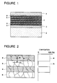
- Fig. 1 is an illustrative cross sectional view of a hard composite material for tool coating including a ultrafine particle-layered film according to the present invention.
- Fig. 2 is an enlarged illustrative cross sectional view of a ultrafine particle-layered film according to the present invention.
- Fig. 3 is a view similar to Fig. 2 but in which the ultrafine particle-layered film has a composition modulated layer.
- Fig. 4 is a view similar to Fig. 2 but in which the ultrafine particle-layered film has a mixed layer.
- Fig. 5 illustrates first embodiment of an apparatus for preparing the ultrafine particle-layered film according to the present invention.
- Fig. 6 illustrates second embodiment of the apparatus for preparing the ultrafine particle-layered film according to the present invention.
- Fig. 1 illustrates a cross sectional view of a hard composite material for tool coating according to the present invention.
- the hard composite material comprises a ultrafine particle-layered film (1) consisting of unit layers (a) and (b) deposited alternatively and repeatedly on a substrate (2).
- An intermediate layer (3) and a surface layer (4) can be formed optionally.
- Each layer (a) or (b) of the ultrafine particle-layered film is emphasized in Fig.
- 1 but its actual thickness is 1 nm to 100 nm, more preferably 1 nm to 50 nm, and more preferably 1 nm to 10 nm, which is about 1/100 of thickness of the intermediate layer (3), which is 0.05 ⁇ m to 5 ⁇ m thick and thickness of the surface layer (4) which is 0.1 ⁇ m to 5 ⁇ m thick respectively.
- Fig. 2 is an illustrative enlarged cross section of the ultrafine particle-layered film (1).
- each layer (a) and (b) of the ultrafine particle-layered film (1) consists of ultrafine particles.
- "d1" and “d2" are particle sizes of particles for each layer (a) and (b).
- a graph shown at right side of Fig.2 illustrates a variation in composition in the ultrafine particle-layered film along the thickness direction.
- the ultrafine particle-layered film according to the present invention have preferably at least one layer made of a compound whose crystal structure is cubic system and at least another one layer made of a compound whose crystal structure is not cubic system and/or is amorphous.
- the compound of non-cubic system is preferably compounds whose crystal structure is hexagonal system.
- the compound whose crystal structure is cubic system is preferably nitride, carbide or carbonitride containing at least one element selected from a group comprising Ti, Zr, Cr, V, Hf, Al and B.
- the compound whose crystal structure is not cubic system or of amorphous is preferably nitride, carbide or carbonitride containing at least one element selected from a group comprising Al, Si and B, in particular aluminium nitride (AlN).
- Particle size of each layer can be nearly equal to a thickness of each layer and/or can be different in two layers. Alignment of the lattices of adjacent particles is not specially required.
- Each layer of the ultrafine particle-layered film according to the present invention can be a composition modulated layer in which composition change gradually and continuously between adjacent two layers or can has a mixed layer of adjacent two layers.
- Fig. 3 and Fig. 4 illustrate structures of the ultrafine particle-layered film having the composition modulated layer and the mixed layer respectively.
- the composition modulated layer or the mixed layer (c) is interposed between adjacent layers (a) and (b).
- each layer of the ultrafine particle-layered film can consist of different elements or can contain common element(s).
- two layers can be TiC and AlN or can be (Ti x Al 1-x )N and (Ti y Al 1-y )N in which 0 ⁇ x, y ⁇ 1 and x ⁇ y.
- the ultrafine particle-layered film can consist of two compounds repeated alternately or of more than three compounds repeated successively.
- at least one compound is a compound having mainly metallic bond property and at least another one compound is a compound having mainly covalent bond property.
- the former is TiN and the later is AlN.
- Lamination cycle can be maintained at a constant value or can be changed regularly or irregularly, if necessary.
- the optimum ratio of unit layers in thickness depends on combination of compounds and properties required in the ultrafine particle-layered film. Generally, the ratio is within 1:10 to 10:1.
- the ultrafine particle-layered film can be prepared by physical vapour deposition (PVD) technique such as sputtering and ion-plating which permits to perform surface-treatment of substrate or tool without deteriorating its inherent strength and high-resistances to wear and breakage.
- PVD physical vapour deposition
- arc-ion plating which can highly ionize material elements is preferably used.
- the arc-ion plating technique permits to increase adhesion to the substrate and to improve crystallinity of a film deposited.
- reactive PVD technique is preferably used.
- a target or plural targets of metal or alloy containing at least one elements selected from IVa, Va, VIa elements, Al, Si and B is used together with a gas containing at least one of C, N and O as materials.
- Other gas than material gas such as inert gas of Ar and He and etchant gas of H2 can be introduced into a film-forming chamber.
- the ultrafine particle-layered film according to the present invention is applied to cutting tools, in particular to cutting tips, it is preferable to coat face and flank of the tip with different ultrafine particle-layered films possessing different lamination cycles which depend to properties required in face and flank respectively.
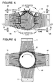
- Fig. 5 is an illustrative view of first embodiment of an apparatus for producing the ultrafine particle-layered film according to the present invention.
- each substrate (12) such as tool or tip is held on a periphery of a rotary holder (15). While the rotary holder (15) is rotated, vapor of Al and Ti are created from two vapour sources (10, 11) and also arc discharge is created by an arc electrode (20) in nitrogen gas atmosphere so that ultra thin films of AlN and TiN are deposited alternately on a surface of the substrate (12).
- a shade or mask (16) is used so as to produce a ultrafine particle-layered film having substantially no composition modulated layer (a/b/a/ - - -).
- a ultrafine particle-layered film (1) (Fig. 1) having a distribution in composition shown in the right side of Fig. 2.is formed on the substrate (2).
- Fig. 6 is an illustrative view of second embodiment of the apparatus for producing the ultrafine particle-layered film according to the present invention.
- This second embodiment differs from the first embodiment in that composition modulated layers (c) can be formed in this case.
- four vapour sources (10, 10', 11, 11') of Al and Ti surround the rotary holder (15) so that the composition modulated layers (c) are formed at zones where both vapor of Ti and Al arrive to produce a nitride of Ti and Al.
- Fig. 3 and Fig. 4 illustrate ultrafine particle-layered films obtained by this embodiment and each graph shown at the right side of these figures shows a distribution in components of the resulting ultrafine particle-layered film.
- At least one intermediate layer (3) having a thickness of 0.05 ⁇ m to 5 ⁇ m is preferably interposed between the substrate (2) and the ultrafine particle-layered film (1).
- This intermediate layer (3) is preferably made of a material selected from a group comprising boride, nitride, carbide and oxide of IVa, Va and VIa elements and their solid solutions.
- the intermediate layer (3) functions to increase adhesion between the ultrafine particle-layered film (1) and the substrate (2).
- Such intermediate layer is expected to reduce residual stress in the film deposited on a substrate which differs from the film in its property by assuring gradual control of its properties.
- a surface layer (4) having a thickness of 0.1 ⁇ m to 5 ⁇ m can be deposited on an outer surface of the ultrafine particle-layered film (1).
- the surface layer (4) is preferably made of a material selected from a group comprising nitride, carbide, carbonitride and oxide of IVa, Va and VIa elements.
- Nitride, carbide, carbonitride and oxide of IVa, Va and VIa elements are very hard so that they are expected to be used as wear-resisting coating materials.
- the present invention is characterized in that at least two compounds are deposited alternately in a form of ultrafine particle-layered film consisting of a plurality layers each having a thickness of nanometer order and consisting of fine particles possessing particle size of nanomcter order.
- the ultrafine particle-layered film shows improved strength, wear-resistance, tenacity and resistance to breakage.
- the thickness of each layer is not higher than 1nm, to ensure that a stratified structure is maintained.
- the advantages of the present invention cannot be guaranteed even if diffusion of consistent elements is reduced to very low level if the thickness is not higher than 1 nm. If the thickness of each layer exceeeds 100 nm, the effect to prevent dislocation can be lost. Therefore, the thickness of each layer is preferably in a range of 1 nm to 50 nm.
- the particle size of particles of which each layer is made is not higher than 1 nm, structure of each particle can become very unstable and a particulate structure could disappear due to diffusion, or the particle size increases due to recombination of adjacent particles so that the resulting particle has a particle size of higher than 1 nm.
- the remarkable advantages in wear-resistance is thus not always apparent even if fine particles having particle sizes of lower than 1 nm are produced.
- the particle size exceeds 100 nm, the effects to prevent dislocation and crack tends to be lowered. Therefore, it is preferable to select the particle size of each particle in a range of 1 nm to 50 nm.
- the choice of particle size will overall depend on applications and quantity criteria, and need not necessarily be confined to these ranges.
- the maximum particle size is preferably the same value as the thickness, is at most about 1.1 times of the thickness or less.
- Japanese patent laid-open No. 5-80547 discloses a multi-layered protective film or fine particle dispersion film.
- the protective film must have an interface which is coherent to lattices of crystals.
- the above-mentioned advantages can be realized only when two of the stratified structure and the ultrafine particle structure are realized simultaneously. In other words, the above-mentioned advantages can not be obtained by one of the stratified structure and the ultrafine particle structure alone.
- the ultrafine particle-layered film according to the present invention is advantageously formed on a tool having a substrate made of CBN sintered body, diamond sintered body, silicon nitride sintered body, aluminium oxide-titanium carbide sintered body cemented carbide, cermets or high speed steel at least a portion where cutting is effected, so as to improve wear-resistance, machinability and fracture-resistance and to increase tool life.
- one layer to be stratified has a crystal structure of cubic system and another layer has a crystal structure of other than the cubic system and/or is amorphous due to their mechanical properties or anisotropy in mechanical properties caused by anisotropy in crystal structure.
- the crystal structure other than the cubic system is preferably hexagonal.
- Nitride, carbide and carbonitride of Ti, Zr, Cr, V or Hf have a crystal structure of cubic system and possess improved hardness, heat-resistance, resistance to oxidation and chemical resistance. Therefore, these materials are suitable to prepare the ultrafine particle-layered film according to the present invention.
- Nitride, carbide and carbonitride of their alloys or alloy with Al are suitable because it is known that they are better in the above-mentioned properties.
- Cubic boron nitride (CBN) which is a nitride of B is the hardest material next to diamond and possesses higher heat-resistance and oxidation-resistance than diamond. It is easily estimated that alloy compounds between these compounds and B also may possess superior properties. Therefore, these materials also are suitable to prepare the ultrafine particle-layered film according to the present invention
- carbide, nitride or carbonitride of Al, Si or B show improved hardness, chemical stability and heat-resistance.
- AlN possessing hexagonal crystal structure is suitable to combined with the metallic bond compound having cubic system since AlN is improved in the above-mentioned properties and possess covalent bond property.
- AlN has Wurtzite type structure under an equilibrium condition at ambient temperature and pressure but has NaCl type structure at elevated pressure.
- a preferred compound is nitride of Ti and Al, and in particular Ti x Al 1-x N (x > 0.25) having cubic structure and Ti y Al 1-y N (y ⁇ 0.25) having hexagonal structure
- the ultrafine particle-layered film according to the present invention permits to improve wear-resistance, oxidation-resistance, fracture-resistance and resistance to welding and to increase tool life for tools having a substrate made of cemented carbide, cermets and high speed steel.
- the thickness of of the ultrafine particle-layered film is not higher than 0.5 ⁇ m, no improvement in adhesion is observed.
- the thickness of the ultrafine particle-layered film exceeds 15 ⁇ m, adhesion to the substrate become lower because of influence of residual stress in the ultrafine particle-layered film and advantage of the ultrafine particle-layered film can not be expected so that wear-resistance becomes lower. Therefore, the thickness of the ultrafine particle-layered film is preferably in a range of 0.5 ⁇ m to 15 ⁇ m.
- the thickness of the intermediate layer (3) is preferably selected in a range between 0.05 and 5 ⁇ m from the view point of productivity.
- the thickness of the surface layer (4) formed on the ultrafine particle-layered film according to the present invention is preferably in a range between 0.1 ⁇ m and 5 ⁇ m. Improvement in wear-resistance is not observed in a thickness of not higher than 0.1 ⁇ m. Thickness of more than 5 ⁇ m also show no improvement in wear-resistance due to peel-off or other reasons.
- the hard composite material for tools according to the present invention can be shaped or machined into and advantageously used as cutting tools such as tip, drills and end mills. It was confirmed that tools prepared from the hard composite material for tools according to the present invention show surprisingly superior cutting performance and long lives.
- the substrate (2) can be selected from following preferable three CBN sintered bodies (1) to (3):
- the binder contains preferably 1 to 50 % by weight of TiN.
- CBN sintered body of the type (2) can be prepared by adding TiN to a binder disclosed in the Japanese patent patent publication-B-52-43846. Addition of TiN increase adhesion to the laminated film (1) of the present invention.
- CBN sintered body of the type (3) can be prepared by adding TiN to a binder disclosed in the Japanese patent publication-A-59-57967. Addition of TiN increase adhesion to the laminated film (1) in this type CBN sintered body also.
- the substrate (2) can be based on diamond sintered bodies containing more than 40 % by volume of diamond:
- the diamond sintered bodies possess particularly higher strength among known diamond sintered bodies and contain at least one member selected from a group comprising iron family element, carbide and carbonitride of IVa, Va and VIa elements, silicon nitride and silicon. It was confirmed also that these materials are effective to bond the ultrafine particle-layered film to the substrate.
- an intermediate layer (3) having a thickness of 0.05 ⁇ m and 5 ⁇ m and made preferably of a material selected from a group comprising boride, nitride, carbide and oxide of IVa, Va and VIa elements and their solid solutions between the substrate (2) and the ultrafine particle-layered film (1) so as to improve bonding strength.
- the substrate (2) can be a silicon nitride sintered body containing 90 % by volume of silicon nitride, preferably prepared by the technique of HIP. Reminding of this silicon nitride sintered body comprise at least one member selected from a group comprising aluminum oxide, aluminum nitride, yttrium oxide, magnesium oxide, hafnium oxide, rear earth and inevitable impurities.
- an intermediate layer (3) having a thickness of 0.05 ⁇ m and 5 ⁇ m and made preferably of a material selected from a group comprising boride, nitride, carbide and carbonitride of IVa, Va and VIa elements is deposited, and then the ultrafine particle-layered film can be deposited by using an apparatus shown in Fig. 5 and Fig. 6.
- TiN can be added to the silicon nitride sintered body so as to improve adhesion to the ultrafine particle-layered film.
- the substrate (2) can be a sintered body made of 20 to 80 % by volume of aluminum oxide and 75 to 15 % by volume of titanium carbide. Reminding of this sintered body can be oxide of at least one element selected from a group comprising Mg, Y, Ca, Zr, Ni and Ti and inevitable impurities.
- a preferable sintered body comprises 65 to 70 % by volume of aluminum oxide and 30 to 25 % by volume of titanium carbide, the remainder being oxide of Mg, Y or Ca and inevitable impurities.
- TiN can be added to the aluminum oxide-titanium carbide sintered body so as to improve adhesion to the ultrafine particle-layered film.
- the hard composite material for tool coating according to the present invention has a layered structure consisting very thin unit layers each consisting of ultrafine particles and which can improve resistances to heat, welding, oxidation, breakage and micro-chipping and improve sliding property, still more, possesses tenacity as well as equal or higher hardness than the conventional hard coats, and can be prepared by PVD technique, so that cutting tools or wear-resisting tools having the hard composite material for tool coating according to the present invention show long tool lives.
- the hard composite material for tool coating according to the present invention can be used to sliding parts whose surface is required to be resistant to wear so as to prolong its life in addition to cutting tools and wear-resisting tools.
- each layer and the particle size of each particle were determined by a transmission electron microscope (TEM), a variation in composition was measured by a micro area energy dispersion type X-ray analyzer (EDX) installed in the transmission electron microscope.
- the variation in composition can be determined by ESCA or SIMS also.
- Crystal structure in the ultrafine particle-layered film was determined from X-ray diffraction pattern and from transmission electron scattering pattern in a micro area by using the transmission electron microscope.
- the X-ray diffraction pattern was obtained by using Cu target and a diffract meter of nickel filter (Cu-K ⁇ , ⁇ -2 ⁇ ).
- a ultrafine particle-layered film according to the present invention was deposited by ion plating with vacuum arc discharge.
- a plurality of targets 10(10'), 11(11') were set in a vacuum chamber and a plurality of the cutting tips (12) were held on a rotary holder (15) arranged at the center of the targets. Thickness and particle size in each layer and variation in composition were controlled by adjusting revolution number of the rotary holder (15), current density of vacuum discharge (evaporation rate of target materials), position and number of the targets and atmosphere pressure.
- argon (Ar) gas was introduced to create a pressure of 10 ⁇ Torr, the tips were heated to 500 °C and a voltage of -1,000 V was applied to the tips to cleaned surface of the tips. After then, argon gas was evacuated.
- N2 gas nitrogen (N2) gas
- CH4 gas and Ar gas was introduced at a rate of 200 cc/min in a function of the revolution number of the rotary holder and of time and simultaneously targets of IVa, Va or VIa elements, Al, silicon or their alloys were vaporized and ionized in arc discharge, so that a reaction product between the target materials and N or C in the gas was deposited on the rotating tips when the tips passes through respective targets.
- sample No. 50 was prepared by known CVD technique in which a combination of TiN and Al2O3 was deposited as a hard coat layer.
- Sample No. 51 layers of TiN and TiAlN were coated by known ion plating with vacuum arc discharge technique on the same tip having the same composition and same shape.
- Sample No. 52 was prepared by known sputtering technique by using two targets of TiC and ZrN.
- Table 1 shows ultrafine particle-layered films (Samples No. 1 to 49) prepared as above.
- Table 2 shows thickness and particle size of each layer were determined by a transmission electron microscope.
- flank wear-resistance tests continuous cutting and intermittent cutting
- the wear-resistance test was effected on following conditions: continuous cutting intermittent cutting test piece SCM 435 SCM435 cutting velocity (m/min) 230 230 feed (mm/rev) 0.35 0.3 cut depth (mm) 2 1.5 cutting time duration (min) 15 20
- Sample No. 1 to 10 reveal that thickness of the ultrafine particle-layered film according to the present invention is preferably in a range of 1 nm to 50 nm.
- Sample No. 11 shows lower wear-resistance because the maximum particle size of a AlN particle in its ultrafine particle-layered film was bigger than a thickness of the layer of AlN, so that no clear stratified structure was observed.
- Sample No. 39 also showed lower wear-resistance because the maximum particle size of particles in CrN layer was only 0.7 nm.
- Sample No. 47 having a composition modulated layer in which proportions of Ti and Al changed continuously interposed between adjacent two layers of TiN and AlN. Same results were observed also in Sample No. 48 having a composition modulated layer in which proportions of TiZr and Cr changed continuously and in Sample No. 49 having a layer of intermediate composition of Hf 0.6 Cr 0.4 N between adjacent two layers of HfN and CrN.
- Powder of TiN and powder of aluminium were mixed at a ratio of 80 : 20 by weight in a pot made of cemented carbide alloy containing balls of the same material to obtain a binder powder.
- Powder of CBN was mixed with the binder powder at a ratio of 70 : 30 by volume and the resulting powder mixture was sintered at 1,400 °C under a pressure of 48 kb for 20 minutes in a container of Mo. The resulting sintered article was shaped into a tip for cutting tool.
- the ultrafine particle-layered film according to the present invention was deposited on the resulting tip as substrate by the same method as Example 1 (Sample No. 101 to 131).
- Sample Nos. 132 to 135 are comparative examples of known cutting tips having the conventional coating layers.
- Sample Nos. 132 and 134 each have a hard coat layer of TiCN layer and/or TiN layer prepared on a tip prepared by the same method as above by ion-plating technique under vacuum arc discharge in usual film forming machine.
- Sample No. 133 has a hard coat layer of a combination of TiN and Al2O3 layer prepared on a tip prepared by the same method as above by usual CVD technique.
- Wear-resistance of the resulting tips was determined by cutting test in which a round steel rod (SUJ2) having a hardness of HRC60 was cut along its periphery at a cutting speed of 150 mm/min, a depth of cut of 0.2 mm, a feed of 0.1 mm per revolution and for 20 minutes in a dry condition to measure a flank wear width (mm). Results are summarized in Table 4.
- the flank wear of this Example was 0.100 mm.
- Example 1 Procedure of Example 1 was repeated but the content (vol %) of CBN in the substrate and compositions (wt %) of binder were changed to those shown in Table 5.
- X-ray diffraction patterns of the resulting sintered articles revealed existence of inevitable contaminations which were thought to be ⁇ -Al2O3, WC and Co.
- the resulting CBN sintered body was shaped into a tip for cutting tool and an intermediate layer of TiN having a thickness of 2 ⁇ m was deposited on portions of the tip where cutting participate by usual PVD technique and then the ultrafine particle-layered film consisting of TiN and AlN deposited alternatively to the total thickness of 5.3 ⁇ m.
- TiN layer had a thickness of 2.5 nm and AlN layer had a thickness of 2.4 nm.
- the film forming apparatus shown in Fig. 5 was used.
- a diamond sintered body was prepared from diamond powder, powder of iron family element, and powder of at least one of carbide or carbonitride of IVa, Va and VIa elements, WC, Si and SiC.
- the content of diamond and combination of powders are summarized in Table 6.
- Material powder mixture was sintered at 1,500 °C under a pressure of 60 kb for 30 minutes in a container of Mo. The resulting sintered article was shaped into a tip for cutting tool.
- an intermediate layer of TiC (3 ⁇ m) was deposited by the same method as Example 2 and then TiN layer and AlN layer were deposited alternately by the same method as Example 2 to obtain ultrafine particle-layered film (thickness of 5.2 ⁇ m). Thickness of each layer was 2.5 nm and the lamination cycle was 5.0 nm. Operation was carried out in the apparatus shown in Fig. 5.
- a silicon nitride sintered body was prepared from a powder mixture of silicon nitride powder, aluminium oxide powder and yttrium oxide powder mixed at proportions by volume of 95 : 3 : 2.
- the powder mixture was sintered by HIP technique at 1,800 °C under a pressure of 300 kg/cm3 for 30 minutes in N2 gas atmosphere.
- the resulting sintered article was shaped into a tip for cutting tool.
- the resulting tips were evaluated by cutting test in which a round steel rod (FC25) was cut along its periphery at a cutting speed of 300 mm/min, a depth of cut of 3 mm, a feed of 0.4 mm per revolution for 15 minutes in dry condition to obtain following flank wear width (mm).
- Tip tested silicon nitride sintered body
- Flank wear width (mm) having no ultrafine particle-layered film 0.185 having ultrafine particle-layered film 0.112
- a aluminium oxide-titanium carbide sintered body was prepared from a powder mixture of aluminium oxide powder, titanium carbide powder and yttrium oxide powder mixed at proportions by volume of 70 : 29.5 : 0.5.
- the powder mixture was sintered at 1,800 °C for 30 minutes.
- the resulting sintered article was shaped into a tip for cutting tool.
- the resulting tips were evaluated by cutting test in which a round Inconel rod (aging treated material: HRC45) was cut along its periphery at a cutting speed of 400 mm/min, a depth of cut of 1.0 mm, a feed of 0.15 mm per revolution for 10 minutes in wet condition to obtain following flank wear width (mm).
- Tip tested aluminium oxide-titanium carbide sintered body
- Flank wear width (mm) having no ultrafine particle-layered film 0.215 having ultrafine particle-layered film 0.098
Landscapes
- Chemical & Material Sciences (AREA)
- Engineering & Computer Science (AREA)
- Ceramic Engineering (AREA)
- Materials Engineering (AREA)
- Organic Chemistry (AREA)
- Structural Engineering (AREA)
- Metallurgy (AREA)
- Chemical Kinetics & Catalysis (AREA)
- Mechanical Engineering (AREA)
- Inorganic Chemistry (AREA)
- Crystallography & Structural Chemistry (AREA)
- Manufacturing & Machinery (AREA)
- Cutting Tools, Boring Holders, And Turrets (AREA)
- Physical Vapour Deposition (AREA)
Abstract
Description
- The present invention relates to a layered film made of ultrafine particles ("ultrafine particles-layered film", hereinafter) for coating cutting tools and a composite material for tools possessing the film which are improved in hardness, strength, wear-resistance and heat-resistance.
- The present invention is advantageously applicable to cutting tools whose substrate is made of CBN sintered body, diamond sintered body, silicon nitride sintered body, aluminum oxide-titanium nitride sintered body, cemented carbide, cermets or high speed tool steel.
- Tools of high speed steel and cemented carbide are coated with a thin film of carbide, nitride or carbonitride of titanium so as to improve wear-resistance. In an application where higher hardness and higher strength at elevated temperatures are required, tools made of sintered body such as cubic boron nitride (CBN) sintered body, diamond sintered body, silicon nitride sintered body and aluminum oxide-titanium carbide are used.
- However, heat-resistance and wear-resistance of known tools are becoming insufficient for recent requirement, so that known cutting tools are difficult to be used in severe cutting conditions including high speed cutting and high performance cutting.
- An object of the present invention is to improve wear-resistance, heat-resistance and corrosion-resistance of cutting tools, wear-resisting tools, sliding parts or machine parts.
- Another object of the present invention is to provide a hard composite material for tools, which possesses higher strength of base material and is improved in wear-resistance, hardness at elevated temperatures and corrosion-resistance, and which can be used in cutting work of hardened steels, high-grade high-hard cast iron or other materials which are difficult to be cut.
- The present invention provides ultrafine particle-layered film, characterized in that the film has more than two layers, each layer is made of a compound consisting mainly of carbide, nitride, carbonitride or oxide of at least one element selected from a group comprising IVa group elements, Va group elements, VIa group elements, Al, Si and B, and each layer is made of ultrafine particles.
- The present invention provides also a hard composite material for tool coating, characterized in that the tool has the ultrafine particle-layered film on at least a portion of a surface of substrate of tool where cutting is effected.
- The ultrafine particle-layered film according to the present invention is based on a novel idea and is different from known concepts. Therefore, the ultrafine particle-layered film and the hard composite material for tool coating according to the present invention will be explained with referring to Fig. 1 and 2.
- Fig. 1 is an illustrative cross sectional view of a hard composite material for tool coating including a ultrafine particle-layered film according to the present invention.
- Fig. 2 is an enlarged illustrative cross sectional view of a ultrafine particle-layered film according to the present invention.
- Fig. 3 is a view similar to Fig. 2 but in which the ultrafine particle-layered film has a composition modulated layer.
- Fig. 4 is a view similar to Fig. 2 but in which the ultrafine particle-layered film has a mixed layer.
- Fig. 5 illustrates first embodiment of an apparatus for preparing the ultrafine particle-layered film according to the present invention.
- Fig. 6 illustrates second embodiment of the apparatus for preparing the ultrafine particle-layered film according to the present invention.
- Fig. 1 illustrates a cross sectional view of a hard composite material for tool coating according to the present invention. The hard composite material comprises a ultrafine particle-layered film (1) consisting of unit layers (a) and (b) deposited alternatively and repeatedly on a substrate (2). An intermediate layer (3) and a surface layer (4) can be formed optionally. Each layer (a) or (b) of the ultrafine particle-layered film is emphasized in Fig. 1 but its actual thickness is 1 nm to 100 nm, more preferably 1 nm to 50 nm, and more preferably 1 nm to 10 nm, which is about 1/100 of thickness of the intermediate layer (3), which is 0.05 µm to 5 µm thick and thickness of the surface layer (4) which is 0.1 µm to 5 µm thick respectively.
- Fig. 2 is an illustrative enlarged cross section of the ultrafine particle-layered film (1). As is seen in Fig, 2, each layer (a) and (b) of the ultrafine particle-layered film (1) consists of ultrafine particles. In Fig. 2, "d₁" and "d₂" are particle sizes of particles for each layer (a) and (b). A graph shown at right side of Fig.2 illustrates a variation in composition in the ultrafine particle-layered film along the thickness direction. One can understand that proportions of elements in two layers "a" (solid line) and "b" (dotted line) are repeated alternately along the thickness direction.
- The ultrafine particle-layered film according to the present invention have preferably at least one layer made of a compound whose crystal structure is cubic system and at least another one layer made of a compound whose crystal structure is not cubic system and/or is amorphous. The compound of non-cubic system is preferably compounds whose crystal structure is hexagonal system.
- The compound whose crystal structure is cubic system is preferably nitride, carbide or carbonitride containing at least one element selected from a group comprising Ti, Zr, Cr, V, Hf, Al and B. The compound whose crystal structure is not cubic system or of amorphous is preferably nitride, carbide or carbonitride containing at least one element selected from a group comprising Al, Si and B, in particular aluminium nitride (AlN).
- Particle size of each layer can be nearly equal to a thickness of each layer and/or can be different in two layers. Alignment of the lattices of adjacent particles is not specially required.
- Each layer of the ultrafine particle-layered film according to the present invention can be a composition modulated layer in which composition change gradually and continuously between adjacent two layers or can has a mixed layer of adjacent two layers.
- Fig. 3 and Fig. 4 illustrate structures of the ultrafine particle-layered film having the composition modulated layer and the mixed layer respectively. The composition modulated layer or the mixed layer (c) is interposed between adjacent layers (a) and (b).
- The compound from which each layer of the ultrafine particle-layered film is made can consist of different elements or can contain common element(s). For example, two layers can be TiC and AlN or can be (Ti x Al 1-x)N and (Ti y Al 1-y )N in which 0 ≦ x, y ≦ 1 and x ≠ y.
- The ultrafine particle-layered film can consist of two compounds repeated alternately or of more than three compounds repeated successively. Preferably, at least one compound is a compound having mainly metallic bond property and at least another one compound is a compound having mainly covalent bond property. For example, preferably, the former is TiN and the later is AlN.
- Lamination cycle can be maintained at a constant value or can be changed regularly or irregularly, if necessary. "Lamination cycle" is a distance between one layer and next layer of the same compound (a). In case of Fig. 2, the lamination cycle is a repeating unit of successive two layers (a) and (b) and is a sum λ of their thickness [ λ = (a) + (b) ].
- The optimum ratio of unit layers in thickness (for example, a ratio of thickness of (a) to (b) of Fig. 1) depends on combination of compounds and properties required in the ultrafine particle-layered film. Generally, the ratio is within 1:10 to 10:1.
- The ultrafine particle-layered film can be prepared by physical vapour deposition (PVD) technique such as sputtering and ion-plating which permits to perform surface-treatment of substrate or tool without deteriorating its inherent strength and high-resistances to wear and breakage. In PVD, arc-ion plating which can highly ionize material elements is preferably used. The arc-ion plating technique permits to increase adhesion to the substrate and to improve crystallinity of a film deposited.
- In particular, reactive PVD technique is preferably used. In fact, higher ionization rates can be obtain by the reactive PVD technique in which a target or plural targets of metal or alloy containing at least one elements selected from IVa, Va, VIa elements, Al, Si and B is used together with a gas containing at least one of C, N and O as materials. Other gas than material gas, such as inert gas of Ar and He and etchant gas of H₂ can be introduced into a film-forming chamber.
- When the ultrafine particle-layered film according to the present invention is applied to cutting tools, in particular to cutting tips, it is preferable to coat face and flank of the tip with different ultrafine particle-layered films possessing different lamination cycles which depend to properties required in face and flank respectively.
- Fig. 5 is an illustrative view of first embodiment of an apparatus for producing the ultrafine particle-layered film according to the present invention. In this embodiment, each substrate (12) such as tool or tip is held on a periphery of a rotary holder (15). While the rotary holder (15) is rotated, vapor of Al and Ti are created from two vapour sources (10, 11) and also arc discharge is created by an arc electrode (20) in nitrogen gas atmosphere so that ultra thin films of AlN and TiN are deposited alternately on a surface of the substrate (12). In this embodiment, a shade or mask (16) is used so as to produce a ultrafine particle-layered film having substantially no composition modulated layer (a/b/a/ - - -). Or, a ultrafine particle-layered film (1) (Fig. 1) having a distribution in composition shown in the right side of Fig. 2.is formed on the substrate (2).
- Fig. 6 is an illustrative view of second embodiment of the apparatus for producing the ultrafine particle-layered film according to the present invention. This second embodiment differs from the first embodiment in that composition modulated layers (c) can be formed in this case. In fact, four vapour sources (10, 10', 11, 11') of Al and Ti surround the rotary holder (15) so that the composition modulated layers (c) are formed at zones where both vapor of Ti and Al arrive to produce a nitride of Ti and Al. Fig. 3 and Fig. 4 illustrate ultrafine particle-layered films obtained by this embodiment and each graph shown at the right side of these figures shows a distribution in components of the resulting ultrafine particle-layered film.
- At least one intermediate layer (3) having a thickness of 0.05 µm to 5 µm is preferably interposed between the substrate (2) and the ultrafine particle-layered film (1). This intermediate layer (3) is preferably made of a material selected from a group comprising boride, nitride, carbide and oxide of IVa, Va and VIa elements and their solid solutions. The intermediate layer (3) functions to increase adhesion between the ultrafine particle-layered film (1) and the substrate (2). Such intermediate layer is expected to reduce residual stress in the film deposited on a substrate which differs from the film in its property by assuring gradual control of its properties.
- A surface layer (4) having a thickness of 0.1 µm to 5 µm can be deposited on an outer surface of the ultrafine particle-layered film (1). The surface layer (4) is preferably made of a material selected from a group comprising nitride, carbide, carbonitride and oxide of IVa, Va and VIa elements.
- Nitride, carbide, carbonitride and oxide of IVa, Va and VIa elements are very hard so that they are expected to be used as wear-resisting coating materials. The present invention is characterized in that at least two compounds are deposited alternately in a form of ultrafine particle-layered film consisting of a plurality layers each having a thickness of nanometer order and consisting of fine particles possessing particle size of nanomcter order. The ultrafine particle-layered film shows improved strength, wear-resistance, tenacity and resistance to breakage.
- According to the present invention, it is believed that, by laminating more than two compounds each having different mechanical properties such as elastic constants and Poisson's ratios and each consisting of fine particles having particle sizes of nanometer order so that each layer has a thickness of nanometer order, resistance to propagation of dislocation in each layer can be increased or dislocations is prevented, or dislocations which propagate between adjacent layers or adjacent particles can be arrested at the interface of adjacent layers and/or at grain boundary, so that plastic deformation of the film can be decreased. Development of crack can be arrested at the interfaces so that fracture-resistance of the film is improved.
- Preferably, the thickness of each layer is not higher than 1nm, to ensure that a stratified structure is maintained. The advantages of the present invention cannot be guaranteed even if diffusion of consistent elements is reduced to very low level if the thickness is not higher than 1 nm. If the thickness of each layer exceeeds 100 nm, the effect to prevent dislocation can be lost. Therefore, the thickness of each layer is preferably in a range of 1 nm to 50 nm.
- Still more, if the particle size of particles of which each layer is made is not higher than 1 nm, structure of each particle can become very unstable and a particulate structure could disappear due to diffusion, or the particle size increases due to recombination of adjacent particles so that the resulting particle has a particle size of higher than 1 nm. The remarkable advantages in wear-resistance is thus not always apparent even if fine particles having particle sizes of lower than 1 nm are produced. On the contrary, if the particle size exceeds 100 nm, the effects to prevent dislocation and crack tends to be lowered. Therefore, it is preferable to select the particle size of each particle in a range of 1 nm to 50 nm. However, the choice of particle size will overall depend on applications and quantity criteria, and need not necessarily be confined to these ranges.
- There is no special limitation in a relation between the thickness of each layer and the particle size. However, excessive growth of a particle over a thickness result in disorder of stratified structure. Therefore, the maximum particle size is preferably the same value as the thickness, is at most about 1.1 times of the thickness or less.
- Japanese patent laid-open No. 5-80547 discloses a multi-layered protective film or fine particle dispersion film. In this patent, however, the protective film must have an interface which is coherent to lattices of crystals. In the present invention, the above-mentioned advantages can be realized only when two of the stratified structure and the ultrafine particle structure are realized simultaneously. In other words, the above-mentioned advantages can not be obtained by one of the stratified structure and the ultrafine particle structure alone.
- Still more, in the present invention, coherency to lattices of crystals at interface is not required and, in some cases, there is such danger that advantages of the present invention are lost if an interface between particles in a layer is coherent. In other words, the present invention is different from the idea disclosed in Japanese patent laid-open No. 5-80547 in which existence of coherent interface is indispensable.
- Therefore, the ultrafine particle-layered film according to the present invention is advantageously formed on a tool having a substrate made of CBN sintered body, diamond sintered body, silicon nitride sintered body, aluminium oxide-titanium carbide sintered body cemented carbide, cermets or high speed steel at least a portion where cutting is effected, so as to improve wear-resistance, machinability and fracture-resistance and to increase tool life.
- The above-mentioned advantages become remarkable when one layer to be stratified has a crystal structure of cubic system and another layer has a crystal structure of other than the cubic system and/or is amorphous due to their mechanical properties or anisotropy in mechanical properties caused by anisotropy in crystal structure. The crystal structure other than the cubic system is preferably hexagonal.
- Nitride, carbide and carbonitride of Ti, Zr, Cr, V or Hf have a crystal structure of cubic system and possess improved hardness, heat-resistance, resistance to oxidation and chemical resistance. Therefore, these materials are suitable to prepare the ultrafine particle-layered film according to the present invention. Nitride, carbide and carbonitride of their alloys or alloy with Al are suitable because it is known that they are better in the above-mentioned properties. Cubic boron nitride (CBN) which is a nitride of B is the hardest material next to diamond and possesses higher heat-resistance and oxidation-resistance than diamond. It is easily estimated that alloy compounds between these compounds and B also may possess superior properties. Therefore, these materials also are suitable to prepare the ultrafine particle-layered film according to the present invention
- As the compound whose crystal structure is not cubic system or amorphous, carbide, nitride or carbonitride of Al, Si or B show improved hardness, chemical stability and heat-resistance. In particular, AlN possessing hexagonal crystal structure is suitable to combined with the metallic bond compound having cubic system since AlN is improved in the above-mentioned properties and possess covalent bond property. AlN has Wurtzite type structure under an equilibrium condition at ambient temperature and pressure but has NaCl type structure at elevated pressure. It is reported that Wurtzite type (hexagonal system) AlN has a property to produce an inclined wave without creating shock wave when it is compressed with impact, resulting in that the ultrafine particle-layered film according to the present invention can be protected from impact damage and hence wear-resistance and breakage-resistance are advantageously improved.
- A preferred compound is nitride of Ti and Al, and in particular TixAl1-xN (x > 0.25) having cubic structure and TiyAl1-yN (y ≦ 0.25) having hexagonal structure
- Compounds improved in oxidation-resistance and chemical stability of the above-mentioned compounds, by adding a small amount of rare earth elements such as yttrium or oxygen, provided that their crystal structure and properties are not influenced badly, are also suitable to improve the properties of the the ultrafine particle-layered film according to the present invention.
- When separation of adjacent layers occur at the interface between adjacent two layers where mechanical properties change, it is preferable to interpose, between adjacent two layers, a composition modulated layer in which composition changes gradually and continuously or a mixed layer in which compounds of adjacent layers are mixed. This solution improves resistance to separation and reduces wear caused by micro flaking.
- Therefore, the ultrafine particle-layered film according to the present invention permits to improve wear-resistance, oxidation-resistance, fracture-resistance and resistance to welding and to increase tool life for tools having a substrate made of cemented carbide, cermets and high speed steel.
- It is known that hardness of a thin film is influenced by the hardness of a substrate on which the thin film is deposited and this influence becomes accelerated greatly with the decrement of thickness of the thin film, so that the hardness of thin film approach to the hardness of substrate. Therefore, it is preferable to use a substrate made of CBN sintered body, diamond sintered body, silicon nitride sintered body or aluminium oxide-titanium carbide sintered body which possesses very high hardness at elevated temperatures, so as to maintain high hardness and to improve wear-resistance of the ultrafine particle-layered film according to the present invention at elevated temperature.
- In the hard composite material for tools according to the present invention, if the thickness of of the ultrafine particle-layered film is not higher than 0.5 µm, no improvement in adhesion is observed. On the contrary, if the thickness of the ultrafine particle-layered film exceeds 15 µm, adhesion to the substrate become lower because of influence of residual stress in the ultrafine particle-layered film and advantage of the ultrafine particle-layered film can not be expected so that wear-resistance becomes lower. Therefore, the thickness of the ultrafine particle-layered film is preferably in a range of 0.5 µm to 15 µm.
- Improvement in adhesion of the intermediate layer (3) is not observed when the thickness thereof is not higher than 0.05 µm and exceeds 5 µm. Therefore, the thickness of the intermediate layer (3) is preferably selected in a range between 0.05 and 5 µm from the view point of productivity. The thickness of the surface layer (4) formed on the ultrafine particle-layered film according to the present invention is preferably in a range between 0.1 µm and 5 µm. Improvement in wear-resistance is not observed in a thickness of not higher than 0.1 µm. Thickness of more than 5 µm also show no improvement in wear-resistance due to peel-off or other reasons.
- The hard composite material for tools according to the present invention can be shaped or machined into and advantageously used as cutting tools such as tip, drills and end mills. It was confirmed that tools prepared from the hard composite material for tools according to the present invention show surprisingly superior cutting performance and long lives.
- In a cutting tip, it is confirmed that the cutting performance and life of the cutting tip increase remarkably when the lamination cycle of the ultrafine particle-layered film at the face is bigger than the lamination cycle at the flank. In a different tip having a different shape and application, the cutting performance and life of the cutting tip increase remarkably when the lamination cycle at the flank is bigger than the lamination cycle at the face. This means that required properties such as wear-resistance and acid-resistance for the face and flank are depend to applications and optimum lamination cycle may be different from each other.
- The substrate (2) can be selected from following preferable three CBN sintered bodies (1) to (3):
- (1) CBN sintered article containing 30 to 90 % by volume of cubic boron nitride (CBN), reminding parts being a binder consisting of at least one member selected from a group comprising nitride, carbide, boride and oxide of IVa, Va and VIa elements and their solid solutions and aluminium compound, and inevitable impurities. The binder consist preferably of 50 to 98 % by weight of at least one member selected from a group comprising TiC, TiN, TiCN, (TiM)C, (TiM)N and (TiM)CN in which M is a transition metal selected from IVa, Va nd VIa elements except Ti and 2 to 50 % by weight of aluminium compound.
- (2) CBN sintered body containing 40 to 95 % by volume of cubic boron nitride (CBN), remaining parts being at least one binder selected from a group comprising TiN, boride and carbide of Co or W, aluminum nitride, aluminum boride and their solid solutions and inevitable impurities. The binder contains preferably 1 to 50 % by weight of TiN.
- (3) CBN sintered body containing more than 90 % by volume of CBN crystalline particles, remaining parts being a binder consisting of boronitride of Ia or IIa elements and TiN and inevitable impurities.
- The binder contains preferably 1 to 50 % by weight of TiN.
- CBN sintered body of the type (1) itself is known and its properties and its production method are described in details in the Japanese patent publication-A-53-77811.
- CBN sintered body of the type (2) can be prepared by adding TiN to a binder disclosed in the Japanese patent patent publication-B-52-43846. Addition of TiN increase adhesion to the laminated film (1) of the present invention.
- CBN sintered body of the type (3) can be prepared by adding TiN to a binder disclosed in the Japanese patent publication-A-59-57967. Addition of TiN increase adhesion to the laminated film (1) in this type CBN sintered body also.
- The substrate (2) can be based on diamond sintered bodies containing more than 40 % by volume of diamond:
- (1) a diamond sintered body containing 50 to 98 % by volume of diamond, the remainder being preferably iron family element and inevitable impurities. The iron family element is preferably Co.
- (2) a diamond sintered body containing 60 to 95 % by volume of diamond, the remainder comprising preferably iron family element at least one member selected from a group comprising carbide and carbonitride of IVa, Va and VIa elements, WC and inevitable impurities.
- (3) a diamond sintered body containing 60 to 98 % by volume of diamond, the remainder comprising preferably silicon carbide, silicon, WC and inevitable impurities.
- The diamond sintered bodies possess particularly higher strength among known diamond sintered bodies and contain at least one member selected from a group comprising iron family element, carbide and carbonitride of IVa, Va and VIa elements, silicon nitride and silicon. It was confirmed also that these materials are effective to bond the ultrafine particle-layered film to the substrate.
- It is preferable to interpose an intermediate layer (3) having a thickness of 0.05 µm and 5 µm and made preferably of a material selected from a group comprising boride, nitride, carbide and oxide of IVa, Va and VIa elements and their solid solutions between the substrate (2) and the ultrafine particle-layered film (1) so as to improve bonding strength.
- The substrate (2) can be a silicon nitride sintered body containing 90 % by volume of silicon nitride, preferably prepared by the technique of HIP. Reminding of this silicon nitride sintered body comprise at least one member selected from a group comprising aluminum oxide, aluminum nitride, yttrium oxide, magnesium oxide, hafnium oxide, rear earth and inevitable impurities.
- Onto the silicon nitride sintered body, an intermediate layer (3) having a thickness of 0.05 µm and 5 µm and made preferably of a material selected from a group comprising boride, nitride, carbide and carbonitride of IVa, Va and VIa elements is deposited, and then the ultrafine particle-layered film can be deposited by using an apparatus shown in Fig. 5 and Fig. 6.
- TiN can be added to the silicon nitride sintered body so as to improve adhesion to the ultrafine particle-layered film.
- The substrate (2) can be a sintered body made of 20 to 80 % by volume of aluminum oxide and 75 to 15 % by volume of titanium carbide. Reminding of this sintered body can be oxide of at least one element selected from a group comprising Mg, Y, Ca, Zr, Ni and Ti and inevitable impurities. A preferable sintered body comprises 65 to 70 % by volume of aluminum oxide and 30 to 25 % by volume of titanium carbide, the remainder being oxide of Mg, Y or Ca and inevitable impurities.
- TiN can be added to the aluminum oxide-titanium carbide sintered body so as to improve adhesion to the ultrafine particle-layered film.
- Thus, the hard composite material for tool coating according to the present invention has a layered structure consisting very thin unit layers each consisting of ultrafine particles and which can improve resistances to heat, welding, oxidation, breakage and micro-chipping and improve sliding property, still more, possesses tenacity as well as equal or higher hardness than the conventional hard coats, and can be prepared by PVD technique, so that cutting tools or wear-resisting tools having the hard composite material for tool coating according to the present invention show long tool lives.
- The hard composite material for tool coating according to the present invention can be used to sliding parts whose surface is required to be resistant to wear so as to prolong its life in addition to cutting tools and wear-resisting tools.
- The present invention will be described in more details referring to Examples, but the present invention is not limited to these Examples.
- In Examples, the thickness of each layer and the particle size of each particle were determined by a transmission electron microscope (TEM), a variation in composition was measured by a micro area energy dispersion type X-ray analyzer (EDX) installed in the transmission electron microscope. The variation in composition can be determined by ESCA or SIMS also.
- Crystal structure in the ultrafine particle-layered film was determined from X-ray diffraction pattern and from transmission electron scattering pattern in a micro area by using the transmission electron microscope. The X-ray diffraction pattern was obtained by using Cu target and a diffract meter of nickel filter (Cu-Kα, θ-2θ).
- On a cutting tip of cemented carbide having a composition of JIS P30 and a shape of ISO SNGN120408, a ultrafine particle-layered film according to the present invention was deposited by ion plating with vacuum arc discharge.
- As is shown in Fig. 5 or Fig. 6, a plurality of targets 10(10'), 11(11') were set in a vacuum chamber and a plurality of the cutting tips (12) were held on a rotary holder (15) arranged at the center of the targets. Thickness and particle size in each layer and variation in composition were controlled by adjusting revolution number of the rotary holder (15), current density of vacuum discharge (evaporation rate of target materials), position and number of the targets and atmosphere pressure.
- In operation, after the vacuum chamber of Fig. 5 or Fig. 6 was evacuated to a pressure of 10⁻⁵ Torr, argon (Ar) gas was introduced to create a pressure of 10⁻ Torr, the tips were heated to 500 °C and a voltage of -1,000 V was applied to the tips to cleaned surface of the tips. After then, argon gas was evacuated. Then, at least one of nitrogen (N₂) gas, CH₄ gas and Ar gas was introduced at a rate of 200 cc/min in a function of the revolution number of the rotary holder and of time and simultaneously targets of IVa, Va or VIa elements, Al, silicon or their alloys were vaporized and ionized in arc discharge, so that a reaction product between the target materials and N or C in the gas was deposited on the rotating tips when the tips passes through respective targets.
- For comparison, the conventional coating films were deposited on tips prepared by the same method (Sample No. 50 to 52). Sample No. 50 was prepared by known CVD technique in which a combination of TiN and Al₂O₃ was deposited as a hard coat layer. In Sample No. 51, layers of TiN and TiAlN were coated by known ion plating with vacuum arc discharge technique on the same tip having the same composition and same shape. Sample No. 52 was prepared by known sputtering technique by using two targets of TiC and ZrN.
- Table 1 shows ultrafine particle-layered films (Samples No. 1 to 49) prepared as above.
- Table 2 shows thickness and particle size of each layer were determined by a transmission electron microscope.
- The results of flank wear-resistance tests (continuous cutting and intermittent cutting) of the resulting tips also are summarized in Table 2. The wear-resistance test was effected on following conditions:
continuous cutting intermittent cutting test piece SCM 435 SCM435 cutting velocity (m/min) 230 230 feed (mm/rev) 0.35 0.3 cut depth (mm) 2 1.5 cutting time duration (min) 15 20 
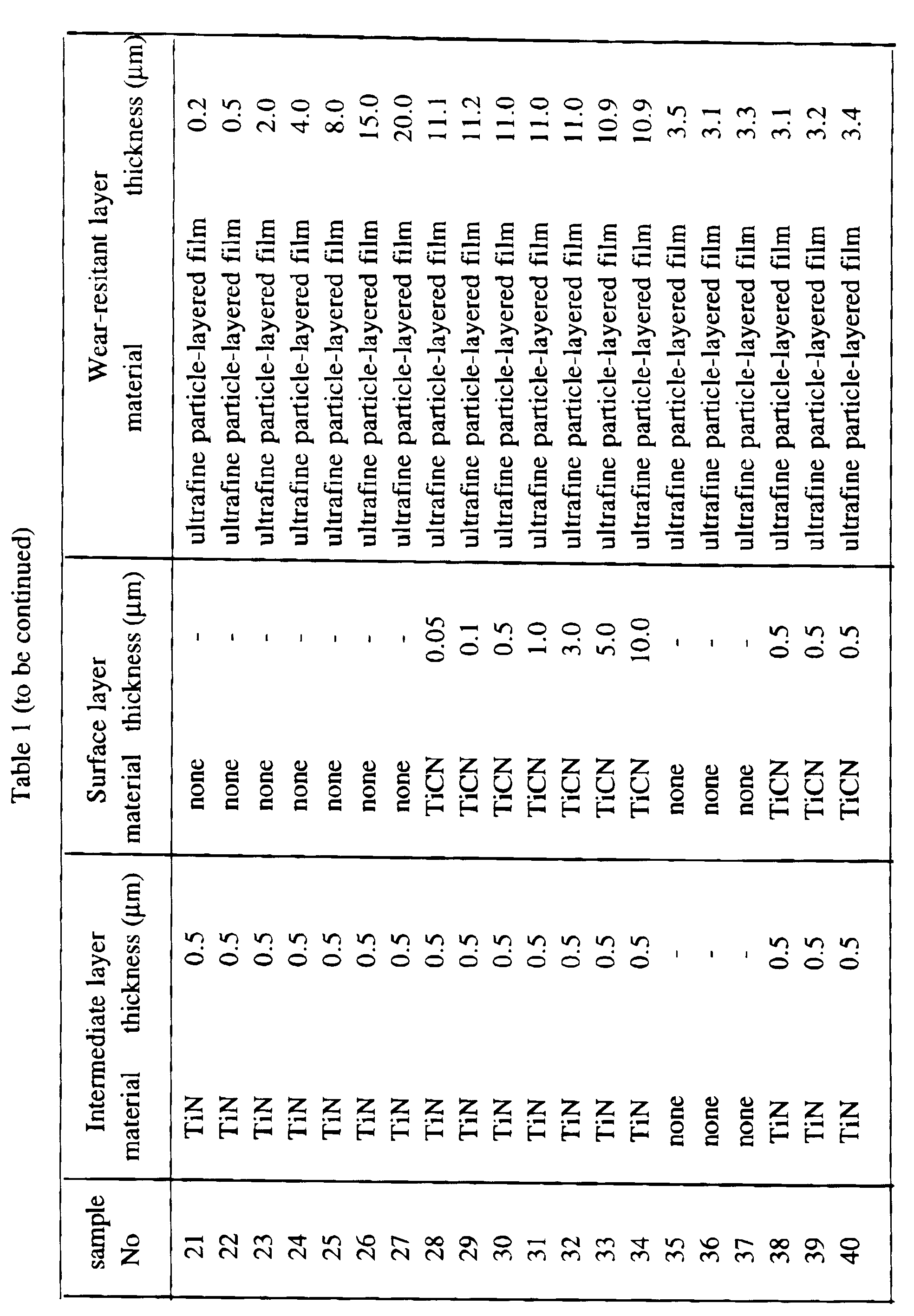

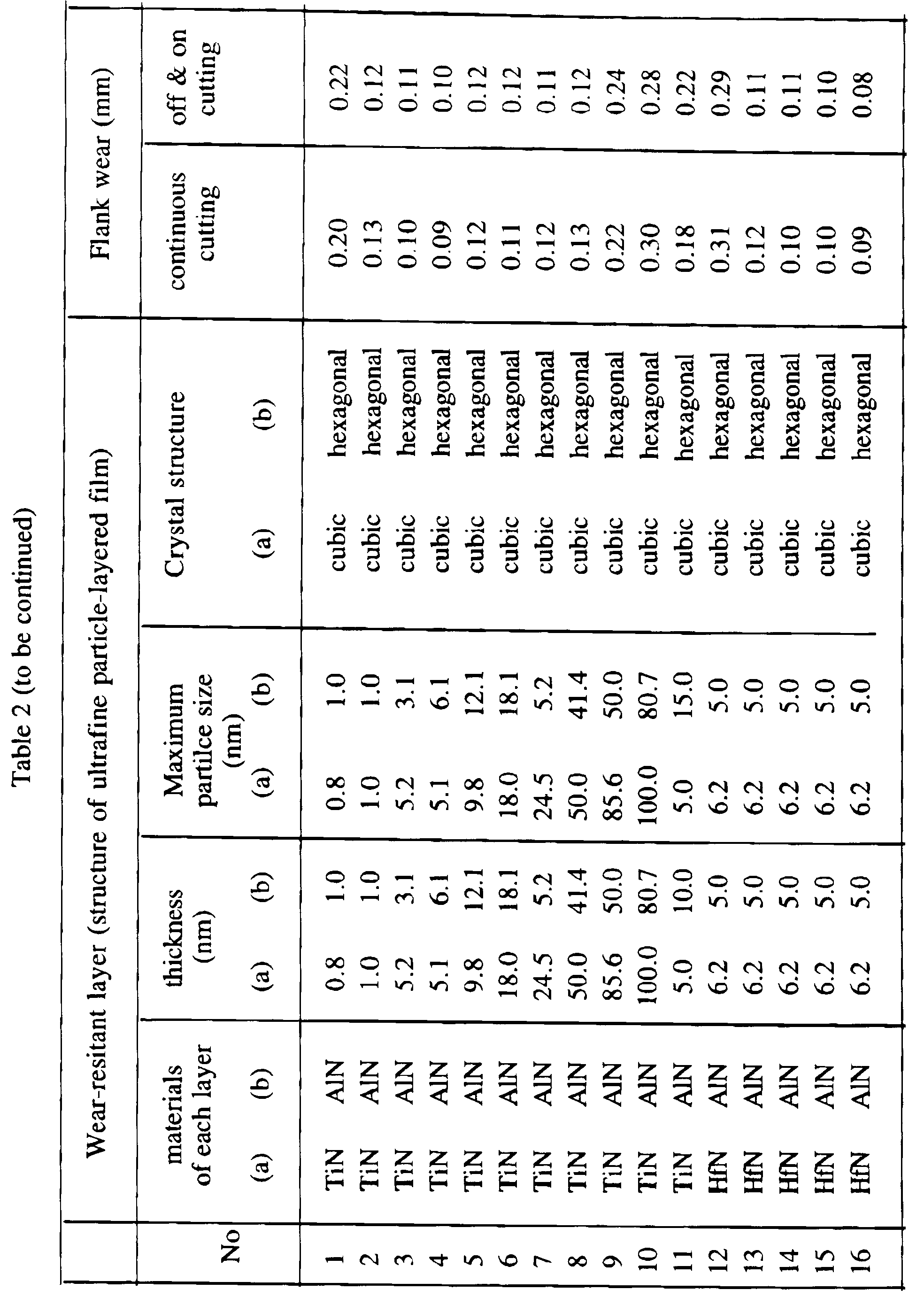


- The results summarized in Table 1 and Table 2 reveal that the conventional tip (Sample No. 50) whose hard coating layer was prepared by the conventional PVD technique has not sufficient resistance to breakage because its base material deteriorate in tenacity. On the contrary, tips according to the present invention (Sample No. 1 to 49) show superior wear-resistance in both of continuous and intermittent cutting operations and also show improved resistance to breakage since their hard coat layers were prepared by PVD technique which can reserve the tenacity of base material.
- The results of Sample No. 1 to 10 reveal that thickness of the ultrafine particle-layered film according to the present invention is preferably in a range of 1 nm to 50 nm. In fact, Sample No. 11 shows lower wear-resistance because the maximum particle size of a AlN particle in its ultrafine particle-layered film was bigger than a thickness of the layer of AlN, so that no clear stratified structure was observed. Sample No. 39 also showed lower wear-resistance because the maximum particle size of particles in CrN layer was only 0.7 nm.
- The results of Sample No. 12 to 20 reveal that the optimum thickness of the intermediate layer is 0.05 µm to 5 µm.
- The results of Sample No. 21 to 27 reveal that preferable total thickness of the ultrafine particle-layered film is 0.5 µm to 15 µm.
- The results of Sample No. 28 to 34 reveal that the optimum thickness of the surface layer is 0.1 µm to 5 µm.
- High wear-resistance and breakage-resistance were observed in Sample No. 47 having a composition modulated layer in which proportions of Ti and Al changed continuously interposed between adjacent two layers of TiN and AlN. Same results were observed also in Sample No. 48 having a composition modulated layer in which proportions of TiZr and Cr changed continuously and in Sample No. 49 having a layer of intermediate composition of Hf0.6Cr0.4N between adjacent two layers of HfN and CrN.
- Powder of TiN and powder of aluminium were mixed at a ratio of 80 : 20 by weight in a pot made of cemented carbide alloy containing balls of the same material to obtain a binder powder. Powder of CBN was mixed with the binder powder at a ratio of 70 : 30 by volume and the resulting powder mixture was sintered at 1,400 °C under a pressure of 48 kb for 20 minutes in a container of Mo. The resulting sintered article was shaped into a tip for cutting tool.
- The ultrafine particle-layered film according to the present invention was deposited on the resulting tip as substrate by the same method as Example 1 (Sample No. 101 to 131).
- For comparison, the conventional coating films were deposited on tips prepared by the same method (Sample No. 132 to 135). The results are summarized in Table 3 and Table 4.
- In Table 3 and Table 4, star mark (*) indicates examples outside the present invention. For example, Sample No. 101 is outside the present invention because its ultrafine particle-laminated film (total thickness of 5.1 µm) has a layer of TiN (0.8 nm) and of AlN (0.9 nm) and of lamination cycle = 1.7 nm.
- Sample Nos. 132 to 135 are comparative examples of known cutting tips having the conventional coating layers.
- Sample Nos. 132 and 134 each have a hard coat layer of TiCN layer and/or TiN layer prepared on a tip prepared by the same method as above by ion-plating technique under vacuum arc discharge in usual film forming machine.
- Sample No. 133 has a hard coat layer of a combination of TiN and Al₂O₃ layer prepared on a tip prepared by the same method as above by usual CVD technique.
- Wear-resistance of the resulting tips was determined by cutting test in which a round steel rod (SUJ2) having a hardness of HRC60 was cut along its periphery at a cutting speed of 150 mm/min, a depth of cut of 0.2 mm, a feed of 0.1 mm per revolution and for 20 minutes in a dry condition to measure a flank wear width (mm). Results are summarized in Table 4.


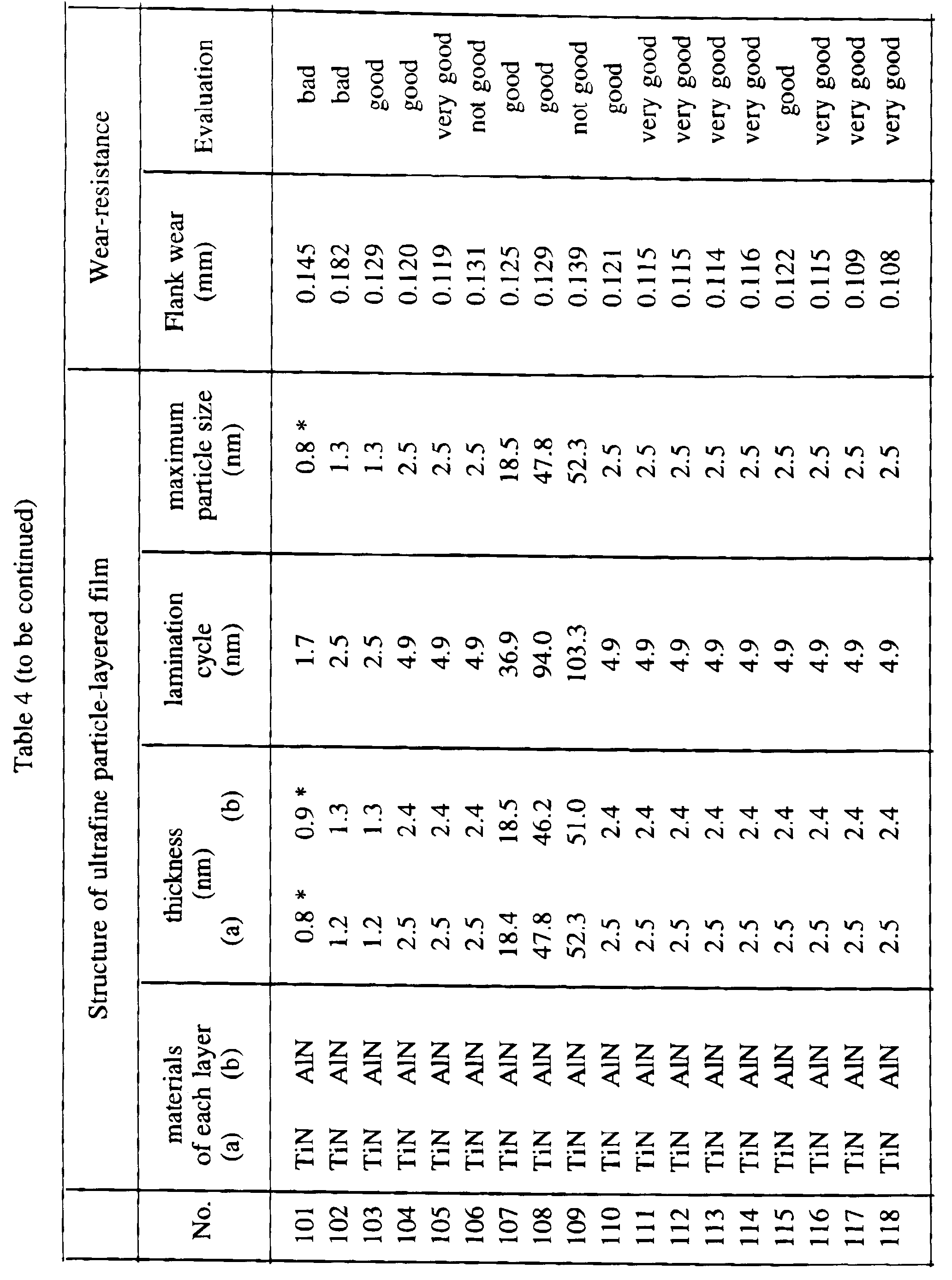

- The procedure of Examples 1 was repeated but a film forming apparatus shown in Fig. 6 was used (totally four targets of Ti and Al were used) and a laminated film was prepared from the same material under the same conditions as Sample No. 118 (TiN layer = 2.5 nm and AlN layer = 2.4 nm).
- The flank wear of this Example was 0.100 mm.
- Procedure of Example 1 was repeated but the content (vol %) of CBN in the substrate and compositions (wt %) of binder were changed to those shown in Table 5. X-ray diffraction patterns of the resulting sintered articles revealed existence of inevitable contaminations which were thought to be α-Al₂O₃, WC and Co.
- The resulting CBN sintered body was shaped into a tip for cutting tool and an intermediate layer of TiN having a thickness of 2 µm was deposited on portions of the tip where cutting participate by usual PVD technique and then the ultrafine particle-layered film consisting of TiN and AlN deposited alternatively to the total thickness of 5.3 µm. TiN layer had a thickness of 2.5 nm and AlN layer had a thickness of 2.4 nm. In operation, the film forming apparatus shown in Fig. 5 was used.
- Table 5 shows time until damage (= a time duration until the tool was damaged: min) which was determined when a round steel rod of carburized hardened SCM415 was cut by the resulting tools along its periphery.

- A diamond sintered body was prepared from diamond powder, powder of iron family element, and powder of at least one of carbide or carbonitride of IVa, Va and VIa elements, WC, Si and SiC. The content of diamond and combination of powders are summarized in Table 6. Material powder mixture was sintered at 1,500 °C under a pressure of 60 kb for 30 minutes in a container of Mo. The resulting sintered article was shaped into a tip for cutting tool.
- On portions of the tip where cutting participate, an intermediate layer of TiC (3 µm) was deposited by the same method as Example 2 and then TiN layer and AlN layer were deposited alternately by the same method as Example 2 to obtain ultrafine particle-layered film (thickness of 5.2 µm). Thickness of each layer was 2.5 nm and the lamination cycle was 5.0 nm. Operation was carried out in the apparatus shown in Fig. 5.
- The resulting tips were evaluated by cutting test in which a round steel rod prepared by a combination of
FCD 600 and 16 % Si - Al alloy (cutting ratio = 1:1) was cut along its periphery at a cutting speed of 200 mm/min, a depth of cut of 0.3 mm, a feed of 0.2 mm per revolution for 20 minutes in wet condition to measure a flank wear width (mm). Results are summarized in Table 6.
- A silicon nitride sintered body was prepared from a powder mixture of silicon nitride powder, aluminium oxide powder and yttrium oxide powder mixed at proportions by volume of 95 : 3 : 2. The powder mixture was sintered by HIP technique at 1,800 °C under a pressure of 300 kg/cm³ for 30 minutes in N₂ gas atmosphere. The resulting sintered article was shaped into a tip for cutting tool.
- On portions of the tip where cutting participate, an intermediate layer of TiN (2 µm) was deposited by CVD technique and then TiN layer (2.5 nm) and AlN layer (2.4 nm) were deposited alternately by the same method as Example 2 to obtain ultrafine particle-layered film (thickness of 7.9 µm). Operation was carried out in the apparams shown in Fig. 5.
- The resulting tips were evaluated by cutting test in which a round steel rod (FC25) was cut along its periphery at a cutting speed of 300 mm/min, a depth of cut of 3 mm, a feed of 0.4 mm per revolution for 15 minutes in dry condition to obtain following flank wear width (mm).
Tip tested (silicon nitride sintered body) Flank wear width (mm) having no ultrafine particle-layered film 0.185 having ultrafine particle-layered film 0.112 - A aluminium oxide-titanium carbide sintered body was prepared from a powder mixture of aluminium oxide powder, titanium carbide powder and yttrium oxide powder mixed at proportions by volume of 70 : 29.5 : 0.5. The powder mixture was sintered at 1,800 °C for 30 minutes. The resulting sintered article was shaped into a tip for cutting tool.
- On portions of the tip where cutting participate, an intermediate layer of TiN (3 µm) was deposited by PVD technique and then TiN layer (2.5 nm) and AlN layer (2.4 nm) were deposited alternately (lamination cycle is 2.4 nm) by the same method as Example 2 to obtain ultrafine particle-layered film (thickness of 6.1 µm). Operation was carried out in the apparatus shown in Fig. 5.
- The resulting tips were evaluated by cutting test in which a round Inconel rod (aging treated material: HRC45) was cut along its periphery at a cutting speed of 400 mm/min, a depth of cut of 1.0 mm, a feed of 0.15 mm per revolution for 10 minutes in wet condition to obtain following flank wear width (mm).
Tip tested (aluminium oxide-titanium carbide sintered body) Flank wear width (mm) having no ultrafine particle-layered film 0.215 having ultrafine particle-layered film 0.098
Claims (31)
Applications Claiming Priority (3)
| Application Number | Priority Date | Filing Date | Title |
|---|---|---|---|
| JP24850394 | 1994-09-16 | ||
| JP24850394 | 1994-09-16 | ||
| JP248503/94 | 1994-09-16 |
Publications (2)
| Publication Number | Publication Date |
|---|---|
| EP0701982A1 true EP0701982A1 (en) | 1996-03-20 |
| EP0701982B1 EP0701982B1 (en) | 2002-07-03 |
Family
ID=17179150
Family Applications (1)
| Application Number | Title | Priority Date | Filing Date |
|---|---|---|---|
| EP95402098A Expired - Lifetime EP0701982B1 (en) | 1994-09-16 | 1995-09-18 | Layered film made of ultrafine particles and a hard composite material for tools possessing the film |
Country Status (3)
| Country | Link |
|---|---|
| US (1) | US5700551A (en) |
| EP (1) | EP0701982B1 (en) |
| DE (1) | DE69527236T2 (en) |
Cited By (39)
| Publication number | Priority date | Publication date | Assignee | Title |
|---|---|---|---|---|
| EP0709483A3 (en) * | 1994-10-28 | 1997-04-23 | Sumitomo Electric Industries | Multilayer material |
| WO1998010120A1 (en) * | 1996-09-03 | 1998-03-12 | Balzers Aktiengesellschaft | Workpiece with wear-protective coating |
| GB2320726A (en) * | 1996-12-25 | 1998-07-01 | Nat Ind Research I Of Nagoya | Sintered material containing titanium aluminium nitride |
| WO1998044163A1 (en) * | 1997-03-27 | 1998-10-08 | Sandvik Ab (Publ) | Multilayered coated cutting tool |
| WO1998048072A1 (en) * | 1997-04-18 | 1998-10-29 | Sandvik Ab (Publ) | Multilayered coated cutting tool |
| WO1998058100A1 (en) * | 1997-06-16 | 1998-12-23 | Robert Bosch Gmbh | Method and device for vacuum-coating a substrate |
| WO1999014391A1 (en) * | 1997-09-12 | 1999-03-25 | Balzers Aktiengesellschaft | Tool with protective layer system |
| WO1999014392A1 (en) * | 1997-09-12 | 1999-03-25 | Balzers Aktiengesellschaft | Tool having a protective layer system |
| WO1999029920A1 (en) * | 1997-12-10 | 1999-06-17 | Sandvik Ab (Publ) | Multilayered pvd coated cutting tool |
| WO1999029921A1 (en) * | 1997-12-10 | 1999-06-17 | Sandvik Ab (Publ) | Multilayered pvd coated cutting tool |
| WO1999040233A1 (en) * | 1998-02-04 | 1999-08-12 | Osg Corporation | Multilayer coated tool |
| US5948716A (en) * | 1996-12-25 | 1999-09-07 | National Industrial Research Institute Of Nagoya | Cubic boron nitride based sintered material and its producing method |
| US6071560A (en) * | 1997-09-12 | 2000-06-06 | Balzers Aktiengesellschaft | Tool with tool body and protective layer system |
| WO2000068453A1 (en) * | 1999-05-06 | 2000-11-16 | Sandvik Ab; (Publ) | Pvd coated cutting tool and method of its production |
| WO2000068457A1 (en) * | 1999-05-06 | 2000-11-16 | Sandvik Ab (Publ) | Inserts for metal cutting purposes |
| WO2001016388A1 (en) * | 1999-09-01 | 2001-03-08 | Sandvik Ab (Publ) | Coated grooving or parting insert |
| WO2001018272A1 (en) * | 1999-09-06 | 2001-03-15 | Sandvik Ab (Publ) | Coated cemented carbide insert |
| US6250855B1 (en) | 1999-03-26 | 2001-06-26 | Sandvik Ab | Coated milling insert |
| EP1118688A1 (en) * | 2000-01-19 | 2001-07-25 | Seco Tools Ab | Coated body with nanocrystalline CVD coating for enhanced edge toughness and reduced friction |
| WO2003078689A1 (en) * | 2002-03-14 | 2003-09-25 | Kennametal Inc. | Nanolayered coated cutting tool and method for making the same |
| EP1382709A1 (en) * | 2002-07-11 | 2004-01-21 | Sumitomo Electric Industries, Ltd. | Coated tool |
| EP1122226A3 (en) * | 1999-12-03 | 2004-01-28 | Sumitomo Electric Industries, Ltd. | Coated PCBN cutting tools |
| DE10305109A1 (en) * | 2003-02-07 | 2004-08-26 | Fraunhofer-Gesellschaft zur Förderung der angewandten Forschung e.V. | Highly electrically insulating coating obtained from an insulating material useful for deposition on building component substrates by a gas sputtering process |
| EP1452621A3 (en) * | 2002-09-04 | 2004-09-08 | Seco Tools Ab | Composite structured wear resistant coating |
| EP1574594A1 (en) * | 2004-03-12 | 2005-09-14 | METAPLAS IONON Oberflächenveredelungstechnik GmbH | A carbon containing hard coating and a method for depositing a hard coating onto a substrate |
| EP1323847A3 (en) * | 2001-12-28 | 2005-09-14 | Seco Tools Ab | Coated cemented carbide body and method for use |
| AT413705B (en) * | 2004-08-02 | 2006-05-15 | Boehlerit Gmbh & Co Kg | CUTTING PLATE WITH A MULTILAYER COATING |
| EP1726686A1 (en) * | 2005-05-26 | 2006-11-29 | Hitachi Tool Engineering Ltd. | Hard-coated member |
| US7357975B2 (en) | 2004-03-12 | 2008-04-15 | Metaplas Ionon Oberflachenveredelungstechnik Gmbh | Carbon-containing hard coating and a method for depositing a hard coating onto a substrate |
| EP1932947A2 (en) | 2006-12-15 | 2008-06-18 | Sandvik Intellectual Property AB | Coated cutting tool |
| WO2008119173A1 (en) * | 2007-03-30 | 2008-10-09 | Innovative Materials Technologies Inc. | Coating |
| US7597951B2 (en) | 2005-03-23 | 2009-10-06 | Sandvik Intellectual Property Ab | Coated cutting tool insert |
| WO2010032137A1 (en) * | 2008-09-17 | 2010-03-25 | Diamond Innovations, Inc. | Cubic boron nitride ceramic composites and methods of making thereof |
| CN102560346A (en) * | 2010-12-24 | 2012-07-11 | 鸿富锦精密工业(深圳)有限公司 | Hard film, product with same, and manufacture method of product |
| EP1195452B2 (en) † | 2000-08-31 | 2016-12-07 | Sumitomo Electric Industries, Ltd. | A tool of a surface-coated boron nitride sintered compact |
| KR20180073572A (en) * | 2015-10-28 | 2018-07-02 | 미쓰비시 마테리알 가부시키가이샤 | Surface-coated cutting tool |
| CN111032261A (en) * | 2017-08-29 | 2020-04-17 | 京瓷株式会社 | Coated tools and cutting tools with the same |
| CN111032260A (en) * | 2017-08-29 | 2020-04-17 | 京瓷株式会社 | Coated tool and cutting tool with the same |
| CN115335164A (en) * | 2020-03-27 | 2022-11-11 | 京瓷株式会社 | Coated cutting tool and cutting tool |
Families Citing this family (92)
| Publication number | Priority date | Publication date | Assignee | Title |
|---|---|---|---|---|
| DE19503070C1 (en) * | 1995-02-01 | 1996-08-14 | Karlsruhe Forschzent | Wear protection layer |
| US6613410B1 (en) * | 1999-09-23 | 2003-09-02 | National Label Company | Extended wrap label |
| US20090255189A1 (en) * | 1998-08-19 | 2009-10-15 | Nanogram Corporation | Aluminum oxide particles |
| US7384680B2 (en) | 1997-07-21 | 2008-06-10 | Nanogram Corporation | Nanoparticle-based power coatings and corresponding structures |
| SE520802C2 (en) | 1997-11-06 | 2003-08-26 | Sandvik Ab | Cutting tool coated with alumina and process for its manufacture |
| DE19756588A1 (en) * | 1997-12-18 | 1999-07-01 | Hartec Ges Fuer Hartstoffe Und | Layer system, process for its production and its use |
| US6287711B1 (en) * | 1998-07-01 | 2001-09-11 | Front Edge Technology, Inc. | Wear-resistant coating and component |
| EP1135541B1 (en) * | 1998-10-23 | 2005-06-08 | Ebara Corporation | Sliding member and manufacturing method therefor |
| SE520716C2 (en) | 1999-05-06 | 2003-08-12 | Sandvik Ab | A process for manufacturing a cutting tool coated with alumina |
| SE521284C2 (en) * | 1999-05-19 | 2003-10-21 | Sandvik Ab | Aluminum oxide coated cutting tool for metalworking |
| US6599062B1 (en) | 1999-06-11 | 2003-07-29 | Kennametal Pc Inc. | Coated PCBN cutting inserts |
| RU2161661C1 (en) * | 1999-08-16 | 2001-01-10 | Падеров Анатолий Николаевич | Method of applying wear-resistant coatings and improvement of durability of parts |
| WO2001032799A1 (en) * | 1999-11-04 | 2001-05-10 | Nanogram Corporation | Particle dispersions |
| EP1132498B1 (en) * | 2000-03-09 | 2008-05-07 | Sulzer Metaplas GmbH | Hard layer coated parts |
| DE10016958A1 (en) * | 2000-04-06 | 2001-10-18 | Widia Gmbh | Process for the production of multilayer layers on substrate bodies and composite material, consisting of a coated substrate body |
| IL137548A (en) * | 2000-07-27 | 2006-08-01 | Cerel Ceramic Technologies Ltd | Wear and thermal resistant material produced from super hard particles bound in a matrix of glassceramic by electrophoretic deposition |
| US6575671B1 (en) * | 2000-08-11 | 2003-06-10 | Kennametal Inc. | Chromium-containing cemented tungsten carbide body |
| US6554548B1 (en) | 2000-08-11 | 2003-04-29 | Kennametal Inc. | Chromium-containing cemented carbide body having a surface zone of binder enrichment |
| US6612787B1 (en) * | 2000-08-11 | 2003-09-02 | Kennametal Inc. | Chromium-containing cemented tungsten carbide coated cutting insert |
| JP3637883B2 (en) * | 2000-08-31 | 2005-04-13 | 住友電気工業株式会社 | Surface coated boron nitride sintered body tool |
| SE0004203D0 (en) * | 2000-11-16 | 2000-11-16 | Haakan Hugosson | A surface coating |
| EP1992717B1 (en) * | 2000-12-28 | 2012-02-15 | Kabushiki Kaisha Kobe Seiko Sho | Use of a target for arc ion plating to form a hard film |
| US7033682B1 (en) * | 2001-12-28 | 2006-04-25 | Ues, Inc. | Coating solutions for titanium and titanium alloy machining |
| KR100707755B1 (en) * | 2002-01-21 | 2007-04-17 | 미츠비시 마테리알 고베 툴스 가부시키가이샤 | Surface-coated cutting tool member exhibiting excellent wear resistance in a high-speed cutting process and a method of forming the hard coating layer on the surface of the cutting tool |
| DE10212383A1 (en) * | 2002-03-20 | 2003-10-16 | Guehring Joerg | Anti-wear layer for rotating machining tools consists of nitrides containing chromium, titanium and aluminum and preferably a small amount of elements for grain refining |
| WO2004000494A1 (en) * | 2002-06-25 | 2003-12-31 | Mitsubishi Materials Corporation | Coated cutting tool member |
| US6906295B2 (en) | 2003-02-20 | 2005-06-14 | National Material L.P. | Foodware with multilayer stick resistant ceramic coating and method of making |
| US6942935B2 (en) * | 2003-03-24 | 2005-09-13 | National Material Ip | Foodware with a tarnish-resistant ceramic coating and method of making |
| US20050112295A1 (en) * | 2003-09-23 | 2005-05-26 | Mikola Grechanyuk | Method to produce microlayer thermostable materials |
| CN100419117C (en) * | 2004-02-02 | 2008-09-17 | 株式会社神户制钢所 | Hard laminated film, method for producing same, and film forming apparatus |
| JP4448342B2 (en) * | 2004-02-02 | 2010-04-07 | 株式会社神戸製鋼所 | Fine crystal hard coating |
| RU2272088C1 (en) * | 2004-07-12 | 2006-03-20 | Уфимский государственный авиационный технический университет | Method of the vacuum-ionic-plasmic deposition of the multilayered composites, containing the complex carbides |
| DE102004042407A1 (en) * | 2004-09-02 | 2006-03-23 | Forschungszentrum Karlsruhe Gmbh | Layered composite with cubic boron nitride |
| SE0402180D0 (en) * | 2004-09-10 | 2004-09-10 | Sandvik Ab | Deposition of Ti1-xAlxN using Bipolar Pulsed Dual Microwave Sputtering |
| SE528671C2 (en) * | 2005-01-31 | 2007-01-16 | Sandvik Intellectual Property | Cemented carbide inserts for toughness requiring short-hole drilling and process for making the same |
| US8679674B2 (en) | 2005-03-25 | 2014-03-25 | Front Edge Technology, Inc. | Battery with protective packaging |
| US7846579B2 (en) | 2005-03-25 | 2010-12-07 | Victor Krasnov | Thin film battery with protective packaging |
| SE529223C2 (en) * | 2005-05-06 | 2007-06-05 | Seco Tools Ab | Coated cutting tool comprising hexagonal h- (Mel, Me2) X phase |
| US8080312B2 (en) | 2006-06-22 | 2011-12-20 | Kennametal Inc. | CVD coating scheme including alumina and/or titanium-containing materials and method of making the same |
| US20080014420A1 (en) * | 2006-07-11 | 2008-01-17 | Ion Technology (Hong Kong) Limited | Surface treatment for titanium or titanium-alloys |
| US7371282B2 (en) * | 2006-07-12 | 2008-05-13 | Northrop Grumman Corporation | Solid solution wide bandgap semiconductor materials |
| CN101583451B (en) * | 2007-01-15 | 2011-06-29 | 住友电工硬质合金株式会社 | cBN sintered body and tools made of cBN sintered body |
| US7862927B2 (en) | 2007-03-02 | 2011-01-04 | Front Edge Technology | Thin film battery and manufacturing method |
| US8870974B2 (en) | 2008-02-18 | 2014-10-28 | Front Edge Technology, Inc. | Thin film battery fabrication using laser shaping |
| US7862627B2 (en) | 2007-04-27 | 2011-01-04 | Front Edge Technology, Inc. | Thin film battery substrate cutting and fabrication process |
| US8080323B2 (en) * | 2007-06-28 | 2011-12-20 | Kennametal Inc. | Cutting insert with a wear-resistant coating scheme exhibiting wear indication and method of making the same |
| US20090004449A1 (en) * | 2007-06-28 | 2009-01-01 | Zhigang Ban | Cutting insert with a wear-resistant coating scheme exhibiting wear indication and method of making the same |
| US8628645B2 (en) | 2007-09-04 | 2014-01-14 | Front Edge Technology, Inc. | Manufacturing method for thin film battery |
| US20090060669A1 (en) * | 2007-09-05 | 2009-03-05 | Sandvik Intellectual Property Ab | Coated drill and a method of making the same |
| US20090074522A1 (en) * | 2007-09-17 | 2009-03-19 | Northwestern University | Reduced-friction coatings |
| EP2072636B1 (en) * | 2007-12-21 | 2016-08-31 | Sandvik Intellectual Property AB | Method of making a coated cutting tool |
| US8092922B2 (en) * | 2008-06-30 | 2012-01-10 | GM Global Technology Operations LLC | Layered coating and method for forming the same |
| CN101643889B (en) * | 2008-08-07 | 2012-10-10 | 三菱重工业株式会社 | Part for rotary machine and its method of manufacture |
| US8021768B2 (en) * | 2009-04-07 | 2011-09-20 | National Material, L.P. | Plain copper foodware and metal articles with durable and tarnish free multiplayer ceramic coating and method of making |
| DE102009037183B4 (en) | 2009-08-12 | 2012-03-22 | Bayerische Motoren Werke Aktiengesellschaft | Method for producing a molded part, in particular a control panel for the passenger compartment of a motor vehicle |
| US8502494B2 (en) | 2009-08-28 | 2013-08-06 | Front Edge Technology, Inc. | Battery charging apparatus and method |
| KR101190324B1 (en) * | 2010-02-11 | 2012-10-11 | 대구텍 유한회사 | Cutting tool |
| CH701726B1 (en) * | 2010-05-11 | 2011-03-15 | Medacta Int Sa | Metal substrate comprises nitride-based ceramic coatings used for the production of the joints of orthopedic implants |
| US8409695B2 (en) | 2010-05-28 | 2013-04-02 | Kennametal Inc. | Multilayer nitride hard coatings |
| DE102010039035A1 (en) | 2010-08-06 | 2012-02-09 | Walter Ag | Cutting tool with multilayer coating |
| DE102010038077B4 (en) * | 2010-10-08 | 2018-05-30 | Msm Krystall Gbr (Vertretungsberechtigte Gesellschafter: Dr. Rainer Schneider, 12165 Berlin; Arno Mecklenburg, 10999 Berlin) | Indexable insert and process for its production |
| US8507082B2 (en) | 2011-03-25 | 2013-08-13 | Kennametal Inc. | CVD coated polycrystalline c-BN cutting tools |
| US8865340B2 (en) | 2011-10-20 | 2014-10-21 | Front Edge Technology Inc. | Thin film battery packaging formed by localized heating |
| TW201321542A (en) * | 2011-11-29 | 2013-06-01 | Chenming Mold Ind Corp | Device for making IC shielding film coating and metal shielding film of IC |
| US9887429B2 (en) | 2011-12-21 | 2018-02-06 | Front Edge Technology Inc. | Laminated lithium battery |
| US8864954B2 (en) | 2011-12-23 | 2014-10-21 | Front Edge Technology Inc. | Sputtering lithium-containing material with multiple targets |
| EP2636764B1 (en) * | 2012-03-07 | 2014-07-09 | Seco Tools Ab | Nanolaminated coated cutting tool |
| KR20130105086A (en) | 2012-03-16 | 2013-09-25 | 현대자동차주식회사 | Piston ring for engine |
| US9257695B2 (en) | 2012-03-29 | 2016-02-09 | Front Edge Technology, Inc. | Localized heat treatment of battery component films |
| US9077000B2 (en) | 2012-03-29 | 2015-07-07 | Front Edge Technology, Inc. | Thin film battery and localized heat treatment |
| KR101351843B1 (en) * | 2012-05-02 | 2014-01-16 | 한국야금 주식회사 | Hard coating film for cutting tools |
| US9159964B2 (en) | 2012-09-25 | 2015-10-13 | Front Edge Technology, Inc. | Solid state battery having mismatched battery cells |
| US8753724B2 (en) | 2012-09-26 | 2014-06-17 | Front Edge Technology Inc. | Plasma deposition on a partially formed battery through a mesh screen |
| US9356320B2 (en) | 2012-10-15 | 2016-05-31 | Front Edge Technology Inc. | Lithium battery having low leakage anode |
| KR101471257B1 (en) | 2012-12-27 | 2014-12-09 | 한국야금 주식회사 | Multilayered thin layer for cutting tools and cutting tools comprising the same |
| JP5618429B2 (en) | 2012-12-28 | 2014-11-05 | 住友電工ハードメタル株式会社 | Surface covering member and manufacturing method thereof |
| JP6143158B2 (en) * | 2012-12-28 | 2017-06-07 | 住友電工ハードメタル株式会社 | Surface covering member and manufacturing method thereof |
| US9028953B2 (en) | 2013-01-11 | 2015-05-12 | Kennametal Inc. | CVD coated polycrystalline c-BN cutting tools |
| JP6043192B2 (en) * | 2013-01-25 | 2016-12-14 | 株式会社神戸製鋼所 | Laminated coating with excellent wear resistance |
| JP2016148101A (en) * | 2015-02-05 | 2016-08-18 | 株式会社神戸製鋼所 | Hard film |
| US10008739B2 (en) | 2015-02-23 | 2018-06-26 | Front Edge Technology, Inc. | Solid-state lithium battery with electrolyte |
| US9994717B2 (en) * | 2015-04-13 | 2018-06-12 | Kennametal Inc. | CVD-coated article and CVD process of making the same |
| KR102144241B1 (en) | 2016-10-25 | 2020-08-12 | 오에스지 가부시키가이샤 | Hard film and hard film covering member |
| DE112018004986T5 (en) * | 2017-09-27 | 2020-06-10 | Kyocera Corporation | COATED TOOL AND CUTTING TOOL THAT HAS THIS |
| US12227827B2 (en) * | 2017-11-29 | 2025-02-18 | Georgia Tech Research Corporation | Methods to impart color and durable properties to substrates |
| JP6813103B2 (en) * | 2018-03-19 | 2021-01-13 | 住友電気工業株式会社 | Surface coating cutting tool |
| CN112930417A (en) * | 2018-10-26 | 2021-06-08 | 欧瑞康表面处理解决方案股份公司普费菲孔 | Vanadium aluminium nitride (VAlN) microalloyed with titanium and/or silicon |
| KR102299610B1 (en) * | 2019-01-30 | 2021-09-08 | 연세대학교 산학협력단 | Transparent Nanolayered Structure Having Improved Wear-resistant and Flexibility |
| JP6969703B2 (en) * | 2019-03-22 | 2021-11-24 | 株式会社Moldino | Cover cutting tool |
| CN111826614B (en) * | 2020-06-11 | 2022-11-08 | 宣城市华菱精工科技股份有限公司 | Intelligent garage anti-corrosion film layer and preparation method thereof |
| WO2022230363A1 (en) * | 2021-04-30 | 2022-11-03 | 住友電気工業株式会社 | Cutting tool and method for manufacturing same |
| CN117127142B (en) * | 2023-10-08 | 2024-08-23 | 鑫钏五金制品(深圳)有限公司 | Antibacterial hard stainless steel cutter and processing technology thereof |
Citations (14)
| Publication number | Priority date | Publication date | Assignee | Title |
|---|---|---|---|---|
| JPS5243846B1 (en) | 1971-07-01 | 1977-11-02 | ||
| JPS5377811A (en) | 1976-12-21 | 1978-07-10 | Sumitomo Electric Ind Ltd | Sintered material for tools of high hardness and its preparation |
| FR2375155A1 (en) * | 1976-12-21 | 1978-07-21 | Sumitomo Electric Industries | |
| FR2448517A1 (en) * | 1979-02-07 | 1980-09-05 | Gen Electric | COATED CEMENTITIOUS CARBIDE PRODUCT |
| JPS58126902A (en) * | 1982-01-22 | 1983-07-28 | Nachi Fujikoshi Corp | Coated cutting tool |
| JPS591103A (en) * | 1982-06-25 | 1984-01-06 | Toshiba Tungaloy Co Ltd | Coated hard tool tip |
| JPS5957967A (en) | 1982-09-27 | 1984-04-03 | 科学技術庁無機材質研究所長 | Manufacturing method of transparent cubic boron nitride dense body |
| EP0113660A2 (en) * | 1983-01-10 | 1984-07-18 | NGK Spark Plug Co. Ltd. | Nitride based cutting tool |
| US4562163A (en) * | 1982-09-27 | 1985-12-31 | National Institute For Researches In Inorganic Materials | Boron nitride complex and process for its preparation, and process for preparing a light-transmitting dense body of cubic system boron nitride |
| JPS6148568A (en) * | 1984-08-09 | 1986-03-10 | Sumitomo Electric Ind Ltd | Tool coated with multilayered hard film |
| EP0197185A2 (en) * | 1985-04-11 | 1986-10-15 | Kernforschungszentrum Karlsruhe Gmbh | Multilayered and highly wear-resistant protective coating of hard material for metallic surfaces or substrates subjected to a high load |
| EP0310042A2 (en) * | 1987-10-01 | 1989-04-05 | Valenite Inc. | A1N coated silicon nitride-based cutting tools |
| JPH0580547A (en) | 1991-09-19 | 1993-04-02 | Toppan Printing Co Ltd | Electrophotographic sensitive composition for color filter and color filter substrate using that |
| EP0592986A1 (en) * | 1992-10-12 | 1994-04-20 | Sumitomo Electric Industries, Limited | Ultra-thin film laminate |
Family Cites Families (3)
| Publication number | Priority date | Publication date | Assignee | Title |
|---|---|---|---|---|
| FR375155A (en) * | 1907-02-28 | 1907-07-02 | Risler & C | Process for forming a new ceramic mass and making pottery objects of all kinds from it |
| JPS5243846A (en) * | 1975-10-03 | 1977-04-06 | Senichi Masuda | Device for electrostatic powder coating |
| US4984940A (en) * | 1989-03-17 | 1991-01-15 | Kennametal Inc. | Multilayer coated cemented carbide cutting insert |
-
1995
- 1995-09-18 US US08/529,840 patent/US5700551A/en not_active Expired - Lifetime
- 1995-09-18 EP EP95402098A patent/EP0701982B1/en not_active Expired - Lifetime
- 1995-09-18 DE DE69527236T patent/DE69527236T2/en not_active Expired - Lifetime
Patent Citations (14)
| Publication number | Priority date | Publication date | Assignee | Title |
|---|---|---|---|---|
| JPS5243846B1 (en) | 1971-07-01 | 1977-11-02 | ||
| JPS5377811A (en) | 1976-12-21 | 1978-07-10 | Sumitomo Electric Ind Ltd | Sintered material for tools of high hardness and its preparation |
| FR2375155A1 (en) * | 1976-12-21 | 1978-07-21 | Sumitomo Electric Industries | |
| FR2448517A1 (en) * | 1979-02-07 | 1980-09-05 | Gen Electric | COATED CEMENTITIOUS CARBIDE PRODUCT |
| JPS58126902A (en) * | 1982-01-22 | 1983-07-28 | Nachi Fujikoshi Corp | Coated cutting tool |
| JPS591103A (en) * | 1982-06-25 | 1984-01-06 | Toshiba Tungaloy Co Ltd | Coated hard tool tip |
| JPS5957967A (en) | 1982-09-27 | 1984-04-03 | 科学技術庁無機材質研究所長 | Manufacturing method of transparent cubic boron nitride dense body |
| US4562163A (en) * | 1982-09-27 | 1985-12-31 | National Institute For Researches In Inorganic Materials | Boron nitride complex and process for its preparation, and process for preparing a light-transmitting dense body of cubic system boron nitride |
| EP0113660A2 (en) * | 1983-01-10 | 1984-07-18 | NGK Spark Plug Co. Ltd. | Nitride based cutting tool |
| JPS6148568A (en) * | 1984-08-09 | 1986-03-10 | Sumitomo Electric Ind Ltd | Tool coated with multilayered hard film |
| EP0197185A2 (en) * | 1985-04-11 | 1986-10-15 | Kernforschungszentrum Karlsruhe Gmbh | Multilayered and highly wear-resistant protective coating of hard material for metallic surfaces or substrates subjected to a high load |
| EP0310042A2 (en) * | 1987-10-01 | 1989-04-05 | Valenite Inc. | A1N coated silicon nitride-based cutting tools |
| JPH0580547A (en) | 1991-09-19 | 1993-04-02 | Toppan Printing Co Ltd | Electrophotographic sensitive composition for color filter and color filter substrate using that |
| EP0592986A1 (en) * | 1992-10-12 | 1994-04-20 | Sumitomo Electric Industries, Limited | Ultra-thin film laminate |
Non-Patent Citations (3)
| Title |
|---|
| DATABASE WPI Section Ch Week 8337, Derwent World Patents Index; Class M22, AN 83-760769 * |
| DATABASE WPI Section Ch Week 8407, Derwent World Patents Index; Class L02, AN 84-039561 * |
| PATENT ABSTRACTS OF JAPAN vol. 010, no. 208 (C - 361) 22 July 1986 (1986-07-22) * |
Cited By (75)
| Publication number | Priority date | Publication date | Assignee | Title |
|---|---|---|---|---|
| EP0709483A3 (en) * | 1994-10-28 | 1997-04-23 | Sumitomo Electric Industries | Multilayer material |
| WO1998010120A1 (en) * | 1996-09-03 | 1998-03-12 | Balzers Aktiengesellschaft | Workpiece with wear-protective coating |
| US6395379B1 (en) | 1996-09-03 | 2002-05-28 | Balzers Aktiengesellschaft | Workpiece with wear-protective coating |
| GB2320726A (en) * | 1996-12-25 | 1998-07-01 | Nat Ind Research I Of Nagoya | Sintered material containing titanium aluminium nitride |
| GB2320726B (en) * | 1996-12-25 | 2000-11-15 | Nat Ind Res I Of Nagoya | Titanium nitride aluminum based sintered material and its production method |
| US5981416A (en) * | 1996-12-25 | 1999-11-09 | National Industrial Research Institute Of Nagoya | Titanium nitride aluminum based sintered material and its production method |
| US5948716A (en) * | 1996-12-25 | 1999-09-07 | National Industrial Research Institute Of Nagoya | Cubic boron nitride based sintered material and its producing method |
| DE19757681C2 (en) * | 1996-12-25 | 2003-06-26 | Nat Ind Res I Of Nagoya Nagoya | Sintered material based on cubic boron nitride and process for its production |
| WO1998044163A1 (en) * | 1997-03-27 | 1998-10-08 | Sandvik Ab (Publ) | Multilayered coated cutting tool |
| WO1998048072A1 (en) * | 1997-04-18 | 1998-10-29 | Sandvik Ab (Publ) | Multilayered coated cutting tool |
| US7942111B2 (en) | 1997-06-16 | 2011-05-17 | Robert Bosch Gmbh | Method and device for vacuum-coating a substrate |
| US6869676B2 (en) | 1997-06-16 | 2005-03-22 | Robert Bosch Gmbh | Method and device for vacuum-coating a substrate |
| WO1998058100A1 (en) * | 1997-06-16 | 1998-12-23 | Robert Bosch Gmbh | Method and device for vacuum-coating a substrate |
| US6372303B1 (en) | 1997-06-16 | 2002-04-16 | Robert Bosch Gmbh | Method and device for vacuum-coating a substrate |
| AU734809B2 (en) * | 1997-06-16 | 2001-06-21 | Robert Bosch Gmbh | Method and device for vacuum-coating a substrate |
| US6274249B1 (en) | 1997-09-12 | 2001-08-14 | Unaxis Balzers Aktiengesellschaft | Tool with tool body and protective layer system |
| WO1999014391A1 (en) * | 1997-09-12 | 1999-03-25 | Balzers Aktiengesellschaft | Tool with protective layer system |
| US6844069B2 (en) | 1997-09-12 | 2005-01-18 | Unaxis Balzers Aktiengesellschaft | Tool with tool body and protective layer system |
| WO1999014392A1 (en) * | 1997-09-12 | 1999-03-25 | Balzers Aktiengesellschaft | Tool having a protective layer system |
| US6071560A (en) * | 1997-09-12 | 2000-06-06 | Balzers Aktiengesellschaft | Tool with tool body and protective layer system |
| US6333099B1 (en) | 1997-12-10 | 2001-12-25 | Sandvik Ab | Multilayered PVD coated cutting tool |
| WO1999029920A1 (en) * | 1997-12-10 | 1999-06-17 | Sandvik Ab (Publ) | Multilayered pvd coated cutting tool |
| WO1999029921A1 (en) * | 1997-12-10 | 1999-06-17 | Sandvik Ab (Publ) | Multilayered pvd coated cutting tool |
| US6309738B1 (en) | 1998-02-04 | 2001-10-30 | Osg Corporation | Hard multilayer coated tool having increased toughness |
| WO1999040233A1 (en) * | 1998-02-04 | 1999-08-12 | Osg Corporation | Multilayer coated tool |
| US6250855B1 (en) | 1999-03-26 | 2001-06-26 | Sandvik Ab | Coated milling insert |
| EP1038989B1 (en) * | 1999-03-26 | 2004-06-16 | Sandvik Aktiebolag | Coated milling insert |
| US6811580B1 (en) | 1999-05-06 | 2004-11-02 | Sandvik Ab | Inserts for metal cutting purposes |
| WO2000068457A1 (en) * | 1999-05-06 | 2000-11-16 | Sandvik Ab (Publ) | Inserts for metal cutting purposes |
| WO2000068453A1 (en) * | 1999-05-06 | 2000-11-16 | Sandvik Ab; (Publ) | Pvd coated cutting tool and method of its production |
| US6627049B2 (en) | 1999-09-01 | 2003-09-30 | Sandvik Ab | Method of making grooving or parting insert |
| WO2001016388A1 (en) * | 1999-09-01 | 2001-03-08 | Sandvik Ab (Publ) | Coated grooving or parting insert |
| USRE40873E1 (en) * | 1999-09-01 | 2009-08-18 | Sandvik Intellectual Property Aktiebolag | Method of making grooving or parting insert |
| US6342291B1 (en) | 1999-09-01 | 2002-01-29 | Sandvik Ab | Coated grooving or parting insert and method of making same |
| WO2001018272A1 (en) * | 1999-09-06 | 2001-03-15 | Sandvik Ab (Publ) | Coated cemented carbide insert |
| US6326093B1 (en) | 1999-09-06 | 2001-12-04 | Sandvik Ab | Cemented carbide insert and method of making same |
| USRE39814E1 (en) * | 1999-09-06 | 2007-09-04 | Sandvik Intellectual Property Ab | Cemented carbide insert and method of making same |
| EP1122226A3 (en) * | 1999-12-03 | 2004-01-28 | Sumitomo Electric Industries, Ltd. | Coated PCBN cutting tools |
| US6472060B1 (en) | 2000-01-19 | 2002-10-29 | Seco Tools Ab | Coated body with nanocrystalline CVD coating for enhanced edge toughness and reduced friction |
| US6652913B2 (en) | 2000-01-19 | 2003-11-25 | Seco Tools Ab | Method of forming a coated body having a nanocrystalline CVD coating of Ti(C,N,O) |
| KR100759073B1 (en) * | 2000-01-19 | 2007-09-19 | 세코 툴스 에이비 | Coated body with nanocrystalline cvd coating for enhanced edge toughness and reduced friction |
| US6620498B2 (en) | 2000-01-19 | 2003-09-16 | Seco Tools Ab | Coated body with nanocrystalline CVD coating for enhanced edge toughness and reduced friction |
| EP1118688A1 (en) * | 2000-01-19 | 2001-07-25 | Seco Tools Ab | Coated body with nanocrystalline CVD coating for enhanced edge toughness and reduced friction |
| EP1195452B2 (en) † | 2000-08-31 | 2016-12-07 | Sumitomo Electric Industries, Ltd. | A tool of a surface-coated boron nitride sintered compact |
| EP1323847A3 (en) * | 2001-12-28 | 2005-09-14 | Seco Tools Ab | Coated cemented carbide body and method for use |
| US6660133B2 (en) | 2002-03-14 | 2003-12-09 | Kennametal Inc. | Nanolayered coated cutting tool and method for making the same |
| US6884499B2 (en) | 2002-03-14 | 2005-04-26 | Kennametal Inc. | Nanolayered coated cutting tool and method for making the same |
| WO2003078689A1 (en) * | 2002-03-14 | 2003-09-25 | Kennametal Inc. | Nanolayered coated cutting tool and method for making the same |
| US8500966B2 (en) | 2002-03-14 | 2013-08-06 | Kennametal Inc. | Nanolayered coated cutting tool and method for making the same |
| AU2003220073B2 (en) * | 2002-03-14 | 2007-02-01 | Kennametal Inc. | Nanolayered coated cutting tool and method for making the same |
| US7060345B2 (en) | 2002-07-11 | 2006-06-13 | Sumitomo Electric Industries, Ltd. | Coated tool |
| EP1382709A1 (en) * | 2002-07-11 | 2004-01-21 | Sumitomo Electric Industries, Ltd. | Coated tool |
| EP1452621A3 (en) * | 2002-09-04 | 2004-09-08 | Seco Tools Ab | Composite structured wear resistant coating |
| US7083868B2 (en) | 2002-09-04 | 2006-08-01 | Seco Tools Ab | Composite structured wear resistant coating |
| DE10305109B4 (en) * | 2003-02-07 | 2010-07-08 | Fraunhofer-Gesellschaft zur Förderung der angewandten Forschung e.V. | Component with an electrically highly insulating layer and method for its production |
| DE10305109B8 (en) * | 2003-02-07 | 2010-11-11 | Fraunhofer-Gesellschaft zur Förderung der angewandten Forschung e.V. | Component with an electrically highly insulating layer and method for its production |
| DE10305109A1 (en) * | 2003-02-07 | 2004-08-26 | Fraunhofer-Gesellschaft zur Förderung der angewandten Forschung e.V. | Highly electrically insulating coating obtained from an insulating material useful for deposition on building component substrates by a gas sputtering process |
| US7357975B2 (en) | 2004-03-12 | 2008-04-15 | Metaplas Ionon Oberflachenveredelungstechnik Gmbh | Carbon-containing hard coating and a method for depositing a hard coating onto a substrate |
| EP1574594A1 (en) * | 2004-03-12 | 2005-09-14 | METAPLAS IONON Oberflächenveredelungstechnik GmbH | A carbon containing hard coating and a method for depositing a hard coating onto a substrate |
| AT413705B (en) * | 2004-08-02 | 2006-05-15 | Boehlerit Gmbh & Co Kg | CUTTING PLATE WITH A MULTILAYER COATING |
| US7597951B2 (en) | 2005-03-23 | 2009-10-06 | Sandvik Intellectual Property Ab | Coated cutting tool insert |
| US7537822B2 (en) | 2005-05-26 | 2009-05-26 | Hitachi Tool Engineering, Ltd. | Hard-coated member |
| EP1726686A1 (en) * | 2005-05-26 | 2006-11-29 | Hitachi Tool Engineering Ltd. | Hard-coated member |
| US8206812B2 (en) | 2006-12-15 | 2012-06-26 | Sandvik Intellectual Property Ab | Coated cutting tool |
| EP1932947A2 (en) | 2006-12-15 | 2008-06-18 | Sandvik Intellectual Property AB | Coated cutting tool |
| WO2008119173A1 (en) * | 2007-03-30 | 2008-10-09 | Innovative Materials Technologies Inc. | Coating |
| US8354353B2 (en) | 2008-09-17 | 2013-01-15 | Diamond Innovations, Inc. | Cubic boron nitride ceramic composites and methods of making thereof |
| WO2010032137A1 (en) * | 2008-09-17 | 2010-03-25 | Diamond Innovations, Inc. | Cubic boron nitride ceramic composites and methods of making thereof |
| CN102560346A (en) * | 2010-12-24 | 2012-07-11 | 鸿富锦精密工业(深圳)有限公司 | Hard film, product with same, and manufacture method of product |
| KR20180073572A (en) * | 2015-10-28 | 2018-07-02 | 미쓰비시 마테리알 가부시키가이샤 | Surface-coated cutting tool |
| EP3369503A4 (en) * | 2015-10-28 | 2019-04-17 | Mitsubishi Materials Corporation | CUTTING TOOL ON SURFACE |
| US10618113B2 (en) | 2015-10-28 | 2020-04-14 | Mitsubishi Materials Corporation | Surface-coated cutting tool |
| CN111032261A (en) * | 2017-08-29 | 2020-04-17 | 京瓷株式会社 | Coated tools and cutting tools with the same |
| CN111032260A (en) * | 2017-08-29 | 2020-04-17 | 京瓷株式会社 | Coated tool and cutting tool with the same |
| CN115335164A (en) * | 2020-03-27 | 2022-11-11 | 京瓷株式会社 | Coated cutting tool and cutting tool |
Also Published As
| Publication number | Publication date |
|---|---|
| DE69527236D1 (en) | 2002-08-08 |
| DE69527236T2 (en) | 2003-03-20 |
| US5700551A (en) | 1997-12-23 |
| EP0701982B1 (en) | 2002-07-03 |
Similar Documents
| Publication | Publication Date | Title |
|---|---|---|
| EP0701982B1 (en) | Layered film made of ultrafine particles and a hard composite material for tools possessing the film | |
| US5853873A (en) | Hard composite material for tools | |
| EP0695731B1 (en) | Super hard composite material for tools | |
| EP1253215B1 (en) | PVD Al2O3 coated cutting tool | |
| EP1099003B1 (en) | Pvd coated cutting tool and method of its production | |
| EP1382709B1 (en) | Coated tool | |
| EP0592986B1 (en) | Ultra-thin film laminate | |
| EP0685572B1 (en) | Coated hard-alloy blade member | |
| EP1122226B2 (en) | Coated pcbn cutting tools | |
| JPH08134629A (en) | Ultrafine particle laminated film and composite high hardness material for tools having the same | |
| JPH08104583A (en) | Composite high hardness material for tools | |
| JPH09174304A (en) | Surface coated cemented carbide cutting tool with excellent chipping resistance | |
| EP0878563B1 (en) | Coated cutting tool member | |
| JP4351521B2 (en) | Surface coated cutting tool | |
| JPH0873289A (en) | Composite high hardness material for tools | |
| JPH02311202A (en) | Covered cutting tool | |
| JP3371823B2 (en) | Surface coated cemented carbide cutting tool with excellent interlayer adhesion with hard coating layer | |
| JPH09262703A (en) | Surface coated cemented carbide cutting tool with excellent hard coating layer adhesion between layers | |
| JPH0919807A (en) | Surface-coated WC-based cemented carbide cutting tool | |
| IL135223A (en) | Aluminum oxide coated cutting tool and processes for the preparation thereof | |
| JPH09277104A (en) | Surface coated cemented carbide cutting tool with excellent hard coating layer adhesion between layers |
Legal Events
| Date | Code | Title | Description |
|---|---|---|---|
| PUAI | Public reference made under article 153(3) epc to a published international application that has entered the european phase |
Free format text: ORIGINAL CODE: 0009012 |
|
| AK | Designated contracting states |
Kind code of ref document: A1 Designated state(s): DE FR GB IT SE |
|
| 17P | Request for examination filed |
Effective date: 19960917 |
|
| 17Q | First examination report despatched |
Effective date: 19970807 |
|
| GRAG | Despatch of communication of intention to grant |
Free format text: ORIGINAL CODE: EPIDOS AGRA |
|
| GRAG | Despatch of communication of intention to grant |
Free format text: ORIGINAL CODE: EPIDOS AGRA |
|
| GRAH | Despatch of communication of intention to grant a patent |
Free format text: ORIGINAL CODE: EPIDOS IGRA |
|
| GRAH | Despatch of communication of intention to grant a patent |
Free format text: ORIGINAL CODE: EPIDOS IGRA |
|
| GRAH | Despatch of communication of intention to grant a patent |
Free format text: ORIGINAL CODE: EPIDOS IGRA |
|
| GRAA | (expected) grant |
Free format text: ORIGINAL CODE: 0009210 |
|
| AK | Designated contracting states |
Kind code of ref document: B1 Designated state(s): DE FR GB IT SE |
|
| REF | Corresponds to: |
Ref document number: 69527236 Country of ref document: DE Date of ref document: 20020808 |
|
| ET | Fr: translation filed | ||
| PLBE | No opposition filed within time limit |
Free format text: ORIGINAL CODE: 0009261 |
|
| STAA | Information on the status of an ep patent application or granted ep patent |
Free format text: STATUS: NO OPPOSITION FILED WITHIN TIME LIMIT |
|
| 26N | No opposition filed |
Effective date: 20030404 |
|
| PGFP | Annual fee paid to national office [announced via postgrant information from national office to epo] |
Ref country code: DE Payment date: 20140911 Year of fee payment: 20 |
|
| PGFP | Annual fee paid to national office [announced via postgrant information from national office to epo] |
Ref country code: SE Payment date: 20140911 Year of fee payment: 20 Ref country code: GB Payment date: 20140917 Year of fee payment: 20 |
|
| PGFP | Annual fee paid to national office [announced via postgrant information from national office to epo] |
Ref country code: IT Payment date: 20140807 Year of fee payment: 20 |
|
| PGFP | Annual fee paid to national office [announced via postgrant information from national office to epo] |
Ref country code: FR Payment date: 20140906 Year of fee payment: 20 |
|
| REG | Reference to a national code |
Ref country code: DE Ref legal event code: R071 Ref document number: 69527236 Country of ref document: DE |
|
| REG | Reference to a national code |
Ref country code: GB Ref legal event code: PE20 Expiry date: 20150917 |
|
| PG25 | Lapsed in a contracting state [announced via postgrant information from national office to epo] |
Ref country code: GB Free format text: LAPSE BECAUSE OF EXPIRATION OF PROTECTION Effective date: 20150917 |
|
| REG | Reference to a national code |
Ref country code: SE Ref legal event code: EUG |