EP0701331B1 - Procédé et dispositif de circuit de conversion d'un mot numérique à N-bit en valeur de tension analogique - Google Patents
Procédé et dispositif de circuit de conversion d'un mot numérique à N-bit en valeur de tension analogique Download PDFInfo
- Publication number
- EP0701331B1 EP0701331B1 EP95113593A EP95113593A EP0701331B1 EP 0701331 B1 EP0701331 B1 EP 0701331B1 EP 95113593 A EP95113593 A EP 95113593A EP 95113593 A EP95113593 A EP 95113593A EP 0701331 B1 EP0701331 B1 EP 0701331B1
- Authority
- EP
- European Patent Office
- Prior art keywords
- circuit
- word
- value
- gates
- reference voltage
- Prior art date
- Legal status (The legal status is an assumption and is not a legal conclusion. Google has not performed a legal analysis and makes no representation as to the accuracy of the status listed.)
- Expired - Lifetime
Links
- 238000000034 method Methods 0.000 title claims description 21
- 238000006243 chemical reaction Methods 0.000 title claims description 14
- 239000004973 liquid crystal related substance Substances 0.000 claims description 17
- 238000005516 engineering process Methods 0.000 claims description 10
- 239000010409 thin film Substances 0.000 claims description 10
- 230000015654 memory Effects 0.000 claims description 9
- 230000008569 process Effects 0.000 claims description 7
- 230000000295 complement effect Effects 0.000 claims description 6
- 239000000758 substrate Substances 0.000 claims description 5
- 239000003990 capacitor Substances 0.000 claims description 4
- 239000011159 matrix material Substances 0.000 claims description 4
- 238000011156 evaluation Methods 0.000 description 6
- 230000008901 benefit Effects 0.000 description 5
- 238000010586 diagram Methods 0.000 description 3
- 230000002123 temporal effect Effects 0.000 description 3
- 101150072109 trr1 gene Proteins 0.000 description 3
- 238000004519 manufacturing process Methods 0.000 description 2
- 230000009467 reduction Effects 0.000 description 2
- 230000000717 retained effect Effects 0.000 description 2
- 239000004065 semiconductor Substances 0.000 description 2
- 241001136792 Alle Species 0.000 description 1
- 101100154580 Saccharomyces cerevisiae (strain ATCC 204508 / S288c) TRR2 gene Proteins 0.000 description 1
- 230000003213 activating effect Effects 0.000 description 1
- 229910021417 amorphous silicon Inorganic materials 0.000 description 1
- 230000008859 change Effects 0.000 description 1
- 238000010276 construction Methods 0.000 description 1
- 230000005672 electromagnetic field Effects 0.000 description 1
- 230000010354 integration Effects 0.000 description 1
- 239000000463 material Substances 0.000 description 1
- 229910021420 polycrystalline silicon Inorganic materials 0.000 description 1
- 230000035945 sensitivity Effects 0.000 description 1
- 230000008054 signal transmission Effects 0.000 description 1
- 230000007704 transition Effects 0.000 description 1
- 238000012795 verification Methods 0.000 description 1
Images

Classifications
-
- G—PHYSICS
- G09—EDUCATION; CRYPTOGRAPHY; DISPLAY; ADVERTISING; SEALS
- G09G—ARRANGEMENTS OR CIRCUITS FOR CONTROL OF INDICATING DEVICES USING STATIC MEANS TO PRESENT VARIABLE INFORMATION
- G09G3/00—Control arrangements or circuits, of interest only in connection with visual indicators other than cathode-ray tubes
- G09G3/20—Control arrangements or circuits, of interest only in connection with visual indicators other than cathode-ray tubes for presentation of an assembly of a number of characters, e.g. a page, by composing the assembly by combination of individual elements arranged in a matrix no fixed position being assigned to or needed to be assigned to the individual characters or partial characters
- G09G3/2007—Display of intermediate tones
- G09G3/2011—Display of intermediate tones by amplitude modulation
-
- G—PHYSICS
- G09—EDUCATION; CRYPTOGRAPHY; DISPLAY; ADVERTISING; SEALS
- G09G—ARRANGEMENTS OR CIRCUITS FOR CONTROL OF INDICATING DEVICES USING STATIC MEANS TO PRESENT VARIABLE INFORMATION
- G09G3/00—Control arrangements or circuits, of interest only in connection with visual indicators other than cathode-ray tubes
- G09G3/20—Control arrangements or circuits, of interest only in connection with visual indicators other than cathode-ray tubes for presentation of an assembly of a number of characters, e.g. a page, by composing the assembly by combination of individual elements arranged in a matrix no fixed position being assigned to or needed to be assigned to the individual characters or partial characters
- G09G3/34—Control arrangements or circuits, of interest only in connection with visual indicators other than cathode-ray tubes for presentation of an assembly of a number of characters, e.g. a page, by composing the assembly by combination of individual elements arranged in a matrix no fixed position being assigned to or needed to be assigned to the individual characters or partial characters by control of light from an independent source
- G09G3/36—Control arrangements or circuits, of interest only in connection with visual indicators other than cathode-ray tubes for presentation of an assembly of a number of characters, e.g. a page, by composing the assembly by combination of individual elements arranged in a matrix no fixed position being assigned to or needed to be assigned to the individual characters or partial characters by control of light from an independent source using liquid crystals
- G09G3/3611—Control of matrices with row and column drivers
- G09G3/3685—Details of drivers for data electrodes
- G09G3/3688—Details of drivers for data electrodes suitable for active matrices only
-
- H—ELECTRICITY
- H03—ELECTRONIC CIRCUITRY
- H03M—CODING; DECODING; CODE CONVERSION IN GENERAL
- H03M1/00—Analogue/digital conversion; Digital/analogue conversion
- H03M1/66—Digital/analogue converters
- H03M1/82—Digital/analogue converters with intermediate conversion to time interval
-
- G—PHYSICS
- G09—EDUCATION; CRYPTOGRAPHY; DISPLAY; ADVERTISING; SEALS
- G09G—ARRANGEMENTS OR CIRCUITS FOR CONTROL OF INDICATING DEVICES USING STATIC MEANS TO PRESENT VARIABLE INFORMATION
- G09G2310/00—Command of the display device
- G09G2310/02—Addressing, scanning or driving the display screen or processing steps related thereto
- G09G2310/0243—Details of the generation of driving signals
- G09G2310/0259—Details of the generation of driving signals with use of an analog or digital ramp generator in the column driver or in the pixel circuit
-
- G—PHYSICS
- G09—EDUCATION; CRYPTOGRAPHY; DISPLAY; ADVERTISING; SEALS
- G09G—ARRANGEMENTS OR CIRCUITS FOR CONTROL OF INDICATING DEVICES USING STATIC MEANS TO PRESENT VARIABLE INFORMATION
- G09G2310/00—Command of the display device
- G09G2310/02—Addressing, scanning or driving the display screen or processing steps related thereto
- G09G2310/0264—Details of driving circuits
- G09G2310/027—Details of drivers for data electrodes, the drivers handling digital grey scale data, e.g. use of D/A converters
-
- G—PHYSICS
- G09—EDUCATION; CRYPTOGRAPHY; DISPLAY; ADVERTISING; SEALS
- G09G—ARRANGEMENTS OR CIRCUITS FOR CONTROL OF INDICATING DEVICES USING STATIC MEANS TO PRESENT VARIABLE INFORMATION
- G09G2310/00—Command of the display device
- G09G2310/06—Details of flat display driving waveforms
- G09G2310/066—Waveforms comprising a gently increasing or decreasing portion, e.g. ramp
Definitions
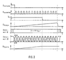
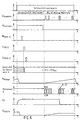
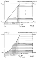
- 6 and 7 each show temporal profiles of the reference voltage U ramp .
- 6 shows a linear ramp-shaped course of the voltage U ramp . Since the times at which the counter word B is decremented are equidistant, the column voltages U column which can be realized are also equidistant.
- the ramp-shaped course of the ramp voltage U ramp is non-linear. As a result, the realizable column voltages U column are irregularly distributed between the minimum value U min and the maximum value U max .
- the resolution of realizable values of the column voltage U column is very high in the range of low voltages.
Landscapes
- Engineering & Computer Science (AREA)
- Theoretical Computer Science (AREA)
- Physics & Mathematics (AREA)
- Computer Hardware Design (AREA)
- General Physics & Mathematics (AREA)
- Chemical & Material Sciences (AREA)
- Crystallography & Structural Chemistry (AREA)
- Analogue/Digital Conversion (AREA)
- Liquid Crystal Display Device Control (AREA)
Claims (9)
- Procédé pour convertir un mot de données numérique à N bits en une valeur de tension analogique par comparaison du mot de données numérique à une tension de référence analogique avec une variation dans le temps en forme de rampe, caractérisé en ce qu'une opération logique ET, NON-ET, OU ou NON-OU du mot de données numérique (A) est réalisée avec un mot de comptage à N bits (B) qui, de manière synchrone avec la variation dans le temps de la tension de référence (URampe), est respectivement décrémenté à partir de sa valeur maximale ("1111") pour une opération ET ou NON-ET et incrémenté à partir de sa valeur minimale ("0000") pour une opération OU ou NON-OU, et en ce que, dès que toutes les sorties de la porte logique délivrent pour la première fois en même temps un "1" logique ou un "0" logique, c'est-à-dire que le mot de comptage (B) atteint une valeur qui correspond au complément (A) du mot de données numérique (A), la valeur de la tension de référence (URampe) alors atteinte est sortie en tant que valeur de tension analogique (USpalte).
- Procédé selon la revendication 1, caractérisé en ce que la variation dans le temps en forme de rampe de la tension de référence (URampe) n'est pas linéaire.
- Procédé selon la revendication 1 ou 2, caractérisé en ce que plusieurs tensions de référence (URampe1, URampe2) avec une variation dans le temps différente peuvent être sélectionnées.
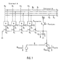
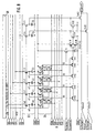
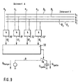
- Agencement de circuit pour convertir un mot de données numérique à N bits en une valeur de tension analogique par comparaison du mot de données numérique à une tension de référence analogique avec une variation dans le temps en forme de rampe selon un procédé selon l'une des revendications 1 à 3, ayant N portes logiques (10' à 13') du même type pour l'opération logique ET, NON-ET, OU ou NON-OU du mot de données numérique (A) avec un mot de comptage à N bits (B), un dispositif pour décrémenter le mot de comptage (B) à partir d'une valeur maximale ("1111") de manière synchrone avec la variation dans le temps de la tension de référence (URampe) si les portes (10' à 13') sont des portes ET ou NON-ET, et un dispositif pour incrémenter le mot de comptage (B) à partir de sa valeur minimale ("0000") de manière synchrone avec la variation dans le temps de la tension de référence (URampe) si les portes (10' à 13') sont des portes OU ou NON-OU, et ayant un circuit d'évaluation (30) pour les signaux de sortie (00'-03') des N portes (10' à 13'), dont le signal de sortie commande la sortie de la valeur de tension de référence (URampe) en tant que valeur de tension analogique de sortie (USpalte).
- Agencement de circuit selon la revendication 4, caractérisé en ce que, en cas d'emploi de portes NON-ET (10'-13'), le circuit d'évaluation (30) présente au moins une capacité (C) et au plus N+3 autres éléments de circuit (S0 à S3, SA, SL, SR).
- Agencement de circuit selon la revendication 5, caractérisé en ce que les au plus N+3 autres éléments de circuit (S0 à S3, SA, SL, SR) sont des commutateurs.
- Agencement de circuit selon l'une des revendications 4 à 6, caractérisé en ce qu'il est réalisé en technologie à couche mince.
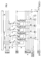
- Circuit de commande numérique pour les lignes de données d'un écran à cristaux liquides avec agencement matriciel de points d'image, lequel comporte, pour chaque ligne de données, une mémoire (22) pour un mot de données numérique (A), un agencement de circuit selon l'une des revendications 4 à 7, et un compteur connecté à tous les agencements de circuit des lignes de données.
- Circuit de commande selon la revendication 8, caractérisé en ce qu'il peut être fabriqué avec la matrice de points d'image de l'écran à cristaux liquides sur un substrat commun et dans un processus commun de technologie à couche mince.
Applications Claiming Priority (2)
| Application Number | Priority Date | Filing Date | Title |
|---|---|---|---|
| DE4432065A DE4432065A1 (de) | 1994-09-09 | 1994-09-09 | Verfahren und Schaltungsanordnung zur Wandlung eines digitalen Datenwortes mit N Bit in einen analogen Spannungswert |
| DE4432065 | 1994-09-09 |
Publications (2)
| Publication Number | Publication Date |
|---|---|
| EP0701331A1 EP0701331A1 (fr) | 1996-03-13 |
| EP0701331B1 true EP0701331B1 (fr) | 2002-02-27 |
Family
ID=6527758
Family Applications (1)
| Application Number | Title | Priority Date | Filing Date |
|---|---|---|---|
| EP95113593A Expired - Lifetime EP0701331B1 (fr) | 1994-09-09 | 1995-08-30 | Procédé et dispositif de circuit de conversion d'un mot numérique à N-bit en valeur de tension analogique |
Country Status (3)
| Country | Link |
|---|---|
| US (1) | US5642117A (fr) |
| EP (1) | EP0701331B1 (fr) |
| DE (2) | DE4432065A1 (fr) |
Families Citing this family (6)
| Publication number | Priority date | Publication date | Assignee | Title |
|---|---|---|---|---|
| TW573165B (en) * | 1999-12-24 | 2004-01-21 | Sanyo Electric Co | Display device |
| US7301520B2 (en) * | 2000-02-22 | 2007-11-27 | Semiconductor Energy Laboratory Co., Ltd. | Image display device and driver circuit therefor |
| JP2002258810A (ja) * | 2001-03-05 | 2002-09-11 | Hitachi Ltd | 液晶表示装置 |
| US7136211B2 (en) * | 2004-11-17 | 2006-11-14 | Intel Corporation | Display device with non-linear ramp |
| US8970573B2 (en) * | 2012-06-27 | 2015-03-03 | Synaptics Incorporated | Voltage interpolating circuit |
| CN119920194B (zh) * | 2025-03-11 | 2025-10-14 | 南京芯视元电子有限公司 | 显示驱动芯片及显示装置 |
Family Cites Families (12)
| Publication number | Priority date | Publication date | Assignee | Title |
|---|---|---|---|---|
| US3267429A (en) * | 1963-09-16 | 1966-08-16 | Honeywell Inc | Digital to pulse comparator apparatus |
| US3422423A (en) * | 1965-01-04 | 1969-01-14 | Sperry Rand Corp | Digital-to-analog converter |
| FR1558504A (fr) * | 1968-01-03 | 1969-02-28 | ||
| US3648275A (en) * | 1970-04-03 | 1972-03-07 | Nasa | Buffered analog converter |
| GB1360943A (en) * | 1972-02-24 | 1974-07-24 | Marconi Co Ltd | Digital-to-analogue converters |
| US4126853A (en) * | 1975-11-05 | 1978-11-21 | Rockwell International Corporation | Non-linear digital-to analog conversion |
| JPS5291638A (en) * | 1976-01-29 | 1977-08-02 | Sony Corp | D/a converter |
| JPS5799821A (en) * | 1980-12-15 | 1982-06-21 | Sony Corp | Digital-to-analogue converter |
| JPS59176985A (ja) * | 1983-03-26 | 1984-10-06 | Citizen Watch Co Ltd | 液晶テレビ受信装置 |
| US4742346A (en) * | 1986-12-19 | 1988-05-03 | Rca Corporation | System for applying grey scale codes to the pixels of a display device |
| FR2622724B1 (fr) * | 1987-10-30 | 1993-02-12 | Thomson Csf | Dispositif de generation de niveaux de brillance sur un ecran de visualisation |
| WO1992007352A1 (fr) * | 1990-10-19 | 1992-04-30 | Thomson S.A. | Circuit de commande pour afficheur de type matriciel et decodeur de signal pour un tel circuit |
-
1994
- 1994-09-09 DE DE4432065A patent/DE4432065A1/de not_active Withdrawn
-
1995
- 1995-08-30 DE DE59510073T patent/DE59510073D1/de not_active Expired - Fee Related
- 1995-08-30 EP EP95113593A patent/EP0701331B1/fr not_active Expired - Lifetime
- 1995-09-05 US US08/523,477 patent/US5642117A/en not_active Expired - Fee Related
Also Published As
| Publication number | Publication date |
|---|---|
| DE59510073D1 (de) | 2002-04-04 |
| DE4432065A1 (de) | 1996-03-14 |
| US5642117A (en) | 1997-06-24 |
| EP0701331A1 (fr) | 1996-03-13 |
Similar Documents
| Publication | Publication Date | Title |
|---|---|---|
| DE69020036T2 (de) | Ansteuerschaltung für ein Matrixanzeigegerät mit Flüssigkristallen. | |
| DE69520915T2 (de) | Als Zeilenwahlabtaster für LCD verwenbares Schieberegister | |
| DE3854163T2 (de) | Verfahren und Schaltung zum Abtasten von kapazitiven Belastungen. | |
| DE60307691T2 (de) | Referenzspannungserzeugungsverfahren und -schaltung, Anzeigesteuerschaltung und Anzeigeeinrichtung mit Gammakorrektur und reduziertem Leistungsverbrauch | |
| DE69838277T2 (de) | Schaltung und verfahren zur ansteuerung einer elektrooptischen vorrichtung, elektrooptisches gerät und dieses verwendende elektronische einrichtung | |
| DE60132540T2 (de) | Anzeige, steuerverfahren dafür und tragbares endgerät | |
| DE69815050T2 (de) | Nichtlinearer Digital-Analog-Wandler und Anzeige | |
| DE4307177C2 (de) | Schaltungsanordnung als Teil eines Schieberegisters zur Ansteuerung von ketten- oder matrixförmig angeordneten Schaltelementen | |
| DE69734491T2 (de) | Potentialerzeugungsvorrichtung | |
| DE69434493T2 (de) | Spannungserzeugungsschaltung, Steuerungsschaltung für gemeinsame Elektrode, Steuerungsschaltung für Signalleitung und Grauskala-Spannungserzeugungsschaltung für Anzeigevorrichtungen | |
| DE102015117758B4 (de) | Schieberegister, ansteuerverfahren und gate-ansteuerschaltung | |
| DE69523910T2 (de) | Schieberegister mit gleich polarisierten mis-transistoren | |
| DE69710766T2 (de) | Bidirektionales schieberegister | |
| DE2810478C2 (fr) | ||
| DE3850059T2 (de) | Sourceelektroden-Ansteuerschaltung für eine Flüssigkristall-Matrixanzeige. | |
| DE69933008T2 (de) | Treiberschaltung für eine elektro-optische vorrichtung, ansteuerungsverfahren, d/a wandler, signaltreiber, elektro-optische anzeigetafel, projektionsanzeigegerät und elektronische vorrichtung | |
| DE102015122140B4 (de) | Gate-Ansteuerschaltung und Ansteuerverfahren für diese | |
| DE3634686A1 (de) | Steuersystem fuer eine elektrolumineszierende bildanzeige | |
| DE102008005855A1 (de) | Flüssigkristallanzeigevorrichtung und Verfahren zum Treiben derselben | |
| DE69117855T2 (de) | Steuerschaltung für ein Anzeigegerät | |
| DE69222959T2 (de) | Verfahren zum Betreiben einer Flüssigkristallanzeigevorrichtung vom Typ der aktiven Matrix | |
| DE3437361A1 (de) | Fluessigkristallanzeige | |
| DE102016124351A1 (de) | Bidirektionale abtasteinheit, ansteuerverfahren und gate-treiberschaltung | |
| DE3526321A1 (de) | Fluessigkristall-anzeigevorrichtung | |
| DE19801263A1 (de) | Niederleistung-Gate-Ansteuerschaltung für Dünnfilmtransistor-Flüssigkristallanzeige unter Verwendung einer elektrischen Ladungs-Recyclingtechnik |
Legal Events
| Date | Code | Title | Description |
|---|---|---|---|
| PUAI | Public reference made under article 153(3) epc to a published international application that has entered the european phase |
Free format text: ORIGINAL CODE: 0009012 |
|
| AK | Designated contracting states |
Kind code of ref document: A1 Designated state(s): DE FR GB NL |
|
| 17P | Request for examination filed |
Effective date: 19960830 |
|
| 17Q | First examination report despatched |
Effective date: 20000118 |
|
| RAP1 | Party data changed (applicant data changed or rights of an application transferred) |
Owner name: UNIVERSITAET STUTTGART |
|
| RIN1 | Information on inventor provided before grant (corrected) |
Inventor name: KULL, STEFAN, DIPL.-ING. Inventor name: LUEDER, ERNST, PROF. DR. ING. HABIL. |
|
| GRAG | Despatch of communication of intention to grant |
Free format text: ORIGINAL CODE: EPIDOS AGRA |
|
| GRAG | Despatch of communication of intention to grant |
Free format text: ORIGINAL CODE: EPIDOS AGRA |
|
| GRAH | Despatch of communication of intention to grant a patent |
Free format text: ORIGINAL CODE: EPIDOS IGRA |
|
| GRAH | Despatch of communication of intention to grant a patent |
Free format text: ORIGINAL CODE: EPIDOS IGRA |
|
| REG | Reference to a national code |
Ref country code: GB Ref legal event code: IF02 |
|
| GRAA | (expected) grant |
Free format text: ORIGINAL CODE: 0009210 |
|
| AK | Designated contracting states |
Kind code of ref document: B1 Designated state(s): DE FR GB NL |
|
| REF | Corresponds to: |
Ref document number: 59510073 Country of ref document: DE Date of ref document: 20020404 |
|
| GBT | Gb: translation of ep patent filed (gb section 77(6)(a)/1977) |
Effective date: 20020423 |
|
| ET | Fr: translation filed | ||
| PLBE | No opposition filed within time limit |
Free format text: ORIGINAL CODE: 0009261 |
|
| STAA | Information on the status of an ep patent application or granted ep patent |
Free format text: STATUS: NO OPPOSITION FILED WITHIN TIME LIMIT |
|
| 26N | No opposition filed |
Effective date: 20021128 |
|
| PGFP | Annual fee paid to national office [announced via postgrant information from national office to epo] |
Ref country code: FR Payment date: 20030711 Year of fee payment: 9 |
|
| PGFP | Annual fee paid to national office [announced via postgrant information from national office to epo] |
Ref country code: GB Payment date: 20030820 Year of fee payment: 9 |
|
| PGFP | Annual fee paid to national office [announced via postgrant information from national office to epo] |
Ref country code: NL Payment date: 20030829 Year of fee payment: 9 Ref country code: DE Payment date: 20030829 Year of fee payment: 9 |
|
| PG25 | Lapsed in a contracting state [announced via postgrant information from national office to epo] |
Ref country code: GB Free format text: LAPSE BECAUSE OF NON-PAYMENT OF DUE FEES Effective date: 20040830 |
|
| PG25 | Lapsed in a contracting state [announced via postgrant information from national office to epo] |
Ref country code: NL Free format text: LAPSE BECAUSE OF NON-PAYMENT OF DUE FEES Effective date: 20050301 Ref country code: DE Free format text: LAPSE BECAUSE OF NON-PAYMENT OF DUE FEES Effective date: 20050301 |
|
| GBPC | Gb: european patent ceased through non-payment of renewal fee |
Effective date: 20040830 |
|
| PG25 | Lapsed in a contracting state [announced via postgrant information from national office to epo] |
Ref country code: FR Free format text: LAPSE BECAUSE OF NON-PAYMENT OF DUE FEES Effective date: 20050429 |
|
| NLV4 | Nl: lapsed or anulled due to non-payment of the annual fee |
Effective date: 20050301 |
|
| REG | Reference to a national code |
Ref country code: FR Ref legal event code: ST |