EP0699246B1 - Apparatus for coating substrates - Google Patents
Apparatus for coating substrates Download PDFInfo
- Publication number
- EP0699246B1 EP0699246B1 EP95911438A EP95911438A EP0699246B1 EP 0699246 B1 EP0699246 B1 EP 0699246B1 EP 95911438 A EP95911438 A EP 95911438A EP 95911438 A EP95911438 A EP 95911438A EP 0699246 B1 EP0699246 B1 EP 0699246B1
- Authority
- EP
- European Patent Office
- Prior art keywords
- substrates
- magnetrons
- reaction producing
- producing means
- vacuum chamber
- Prior art date
- Legal status (The legal status is an assumption and is not a legal conclusion. Google has not performed a legal analysis and makes no representation as to the accuracy of the status listed.)
- Revoked
Links
- 239000000758 substrate Substances 0.000 title claims abstract description 62
- 238000000576 coating method Methods 0.000 title claims abstract description 28
- 239000011248 coating agent Substances 0.000 title claims abstract description 24
- 239000000463 material Substances 0.000 claims abstract description 65
- 238000000151 deposition Methods 0.000 claims abstract description 60
- 238000006243 chemical reaction Methods 0.000 claims abstract description 49
- 230000008021 deposition Effects 0.000 claims description 29
- 239000007789 gas Substances 0.000 claims description 17
- QVGXLLKOCUKJST-UHFFFAOYSA-N atomic oxygen Chemical compound [O] QVGXLLKOCUKJST-UHFFFAOYSA-N 0.000 claims description 9
- 239000001301 oxygen Substances 0.000 claims description 9
- 229910052760 oxygen Inorganic materials 0.000 claims description 9
- 239000000203 mixture Substances 0.000 claims description 3
- OKTJSMMVPCPJKN-UHFFFAOYSA-N Carbon Chemical compound [C] OKTJSMMVPCPJKN-UHFFFAOYSA-N 0.000 claims description 2
- 230000004913 activation Effects 0.000 claims description 2
- 229910052799 carbon Inorganic materials 0.000 claims description 2
- 150000001875 compounds Chemical class 0.000 claims description 2
- IJGRMHOSHXDMSA-UHFFFAOYSA-N Atomic nitrogen Chemical compound N#N IJGRMHOSHXDMSA-UHFFFAOYSA-N 0.000 claims 2
- VNWKTOKETHGBQD-UHFFFAOYSA-N methane Chemical compound C VNWKTOKETHGBQD-UHFFFAOYSA-N 0.000 claims 2
- 239000001257 hydrogen Substances 0.000 claims 1
- 229910052739 hydrogen Inorganic materials 0.000 claims 1
- 125000004435 hydrogen atom Chemical class [H]* 0.000 claims 1
- 229910052757 nitrogen Inorganic materials 0.000 claims 1
- 238000004544 sputter deposition Methods 0.000 abstract description 2
- 230000001143 conditioned effect Effects 0.000 abstract 1
- 238000000926 separation method Methods 0.000 description 4
- 229910052751 metal Inorganic materials 0.000 description 3
- 239000002184 metal Substances 0.000 description 3
- 239000010936 titanium Substances 0.000 description 3
- RTAQQCXQSZGOHL-UHFFFAOYSA-N Titanium Chemical compound [Ti] RTAQQCXQSZGOHL-UHFFFAOYSA-N 0.000 description 2
- 230000006978 adaptation Effects 0.000 description 2
- 229910044991 metal oxide Inorganic materials 0.000 description 2
- 150000004706 metal oxides Chemical class 0.000 description 2
- 230000003287 optical effect Effects 0.000 description 2
- 230000003647 oxidation Effects 0.000 description 2
- 238000007254 oxidation reaction Methods 0.000 description 2
- 238000009416 shuttering Methods 0.000 description 2
- 239000010703 silicon Substances 0.000 description 2
- 229910052710 silicon Inorganic materials 0.000 description 2
- 229910052719 titanium Inorganic materials 0.000 description 2
- XUIMIQQOPSSXEZ-UHFFFAOYSA-N Silicon Chemical compound [Si] XUIMIQQOPSSXEZ-UHFFFAOYSA-N 0.000 description 1
- QCWXUUIWCKQGHC-UHFFFAOYSA-N Zirconium Chemical compound [Zr] QCWXUUIWCKQGHC-UHFFFAOYSA-N 0.000 description 1
- 239000006117 anti-reflective coating Substances 0.000 description 1
- 230000009286 beneficial effect Effects 0.000 description 1
- 239000011247 coating layer Substances 0.000 description 1
- 238000000280 densification Methods 0.000 description 1
- 230000000694 effects Effects 0.000 description 1
- 150000004678 hydrides Chemical class 0.000 description 1
- 238000002955 isolation Methods 0.000 description 1
- 238000001465 metallisation Methods 0.000 description 1
- 229910052758 niobium Inorganic materials 0.000 description 1
- 239000010955 niobium Substances 0.000 description 1
- GUCVJGMIXFAOAE-UHFFFAOYSA-N niobium atom Chemical compound [Nb] GUCVJGMIXFAOAE-UHFFFAOYSA-N 0.000 description 1
- 150000004767 nitrides Chemical class 0.000 description 1
- 150000002926 oxygen Chemical class 0.000 description 1
- 238000005546 reactive sputtering Methods 0.000 description 1
- 238000007789 sealing Methods 0.000 description 1
- 238000000638 solvent extraction Methods 0.000 description 1
- 229910052726 zirconium Inorganic materials 0.000 description 1
Images
Classifications
-
- C—CHEMISTRY; METALLURGY
- C23—COATING METALLIC MATERIAL; COATING MATERIAL WITH METALLIC MATERIAL; CHEMICAL SURFACE TREATMENT; DIFFUSION TREATMENT OF METALLIC MATERIAL; COATING BY VACUUM EVAPORATION, BY SPUTTERING, BY ION IMPLANTATION OR BY CHEMICAL VAPOUR DEPOSITION, IN GENERAL; INHIBITING CORROSION OF METALLIC MATERIAL OR INCRUSTATION IN GENERAL
- C23C—COATING METALLIC MATERIAL; COATING MATERIAL WITH METALLIC MATERIAL; SURFACE TREATMENT OF METALLIC MATERIAL BY DIFFUSION INTO THE SURFACE, BY CHEMICAL CONVERSION OR SUBSTITUTION; COATING BY VACUUM EVAPORATION, BY SPUTTERING, BY ION IMPLANTATION OR BY CHEMICAL VAPOUR DEPOSITION, IN GENERAL
- C23C14/00—Coating by vacuum evaporation, by sputtering or by ion implantation of the coating forming material
- C23C14/22—Coating by vacuum evaporation, by sputtering or by ion implantation of the coating forming material characterised by the process of coating
- C23C14/56—Apparatus specially adapted for continuous coating; Arrangements for maintaining the vacuum, e.g. vacuum locks
- C23C14/568—Transferring the substrates through a series of coating stations
-
- C—CHEMISTRY; METALLURGY
- C23—COATING METALLIC MATERIAL; COATING MATERIAL WITH METALLIC MATERIAL; CHEMICAL SURFACE TREATMENT; DIFFUSION TREATMENT OF METALLIC MATERIAL; COATING BY VACUUM EVAPORATION, BY SPUTTERING, BY ION IMPLANTATION OR BY CHEMICAL VAPOUR DEPOSITION, IN GENERAL; INHIBITING CORROSION OF METALLIC MATERIAL OR INCRUSTATION IN GENERAL
- C23C—COATING METALLIC MATERIAL; COATING MATERIAL WITH METALLIC MATERIAL; SURFACE TREATMENT OF METALLIC MATERIAL BY DIFFUSION INTO THE SURFACE, BY CHEMICAL CONVERSION OR SUBSTITUTION; COATING BY VACUUM EVAPORATION, BY SPUTTERING, BY ION IMPLANTATION OR BY CHEMICAL VAPOUR DEPOSITION, IN GENERAL
- C23C14/00—Coating by vacuum evaporation, by sputtering or by ion implantation of the coating forming material
- C23C14/0021—Reactive sputtering or evaporation
- C23C14/0036—Reactive sputtering
- C23C14/0073—Reactive sputtering by exposing the substrates to reactive gases intermittently
- C23C14/0078—Reactive sputtering by exposing the substrates to reactive gases intermittently by moving the substrates between spatially separate sputtering and reaction stations
-
- C—CHEMISTRY; METALLURGY
- C23—COATING METALLIC MATERIAL; COATING MATERIAL WITH METALLIC MATERIAL; CHEMICAL SURFACE TREATMENT; DIFFUSION TREATMENT OF METALLIC MATERIAL; COATING BY VACUUM EVAPORATION, BY SPUTTERING, BY ION IMPLANTATION OR BY CHEMICAL VAPOUR DEPOSITION, IN GENERAL; INHIBITING CORROSION OF METALLIC MATERIAL OR INCRUSTATION IN GENERAL
- C23C—COATING METALLIC MATERIAL; COATING MATERIAL WITH METALLIC MATERIAL; SURFACE TREATMENT OF METALLIC MATERIAL BY DIFFUSION INTO THE SURFACE, BY CHEMICAL CONVERSION OR SUBSTITUTION; COATING BY VACUUM EVAPORATION, BY SPUTTERING, BY ION IMPLANTATION OR BY CHEMICAL VAPOUR DEPOSITION, IN GENERAL
- C23C14/00—Coating by vacuum evaporation, by sputtering or by ion implantation of the coating forming material
- C23C14/06—Coating by vacuum evaporation, by sputtering or by ion implantation of the coating forming material characterised by the coating material
- C23C14/08—Oxides
-
- C—CHEMISTRY; METALLURGY
- C23—COATING METALLIC MATERIAL; COATING MATERIAL WITH METALLIC MATERIAL; CHEMICAL SURFACE TREATMENT; DIFFUSION TREATMENT OF METALLIC MATERIAL; COATING BY VACUUM EVAPORATION, BY SPUTTERING, BY ION IMPLANTATION OR BY CHEMICAL VAPOUR DEPOSITION, IN GENERAL; INHIBITING CORROSION OF METALLIC MATERIAL OR INCRUSTATION IN GENERAL
- C23C—COATING METALLIC MATERIAL; COATING MATERIAL WITH METALLIC MATERIAL; SURFACE TREATMENT OF METALLIC MATERIAL BY DIFFUSION INTO THE SURFACE, BY CHEMICAL CONVERSION OR SUBSTITUTION; COATING BY VACUUM EVAPORATION, BY SPUTTERING, BY ION IMPLANTATION OR BY CHEMICAL VAPOUR DEPOSITION, IN GENERAL
- C23C14/00—Coating by vacuum evaporation, by sputtering or by ion implantation of the coating forming material
- C23C14/22—Coating by vacuum evaporation, by sputtering or by ion implantation of the coating forming material characterised by the process of coating
- C23C14/50—Substrate holders
- C23C14/505—Substrate holders for rotation of the substrates
-
- C—CHEMISTRY; METALLURGY
- C23—COATING METALLIC MATERIAL; COATING MATERIAL WITH METALLIC MATERIAL; CHEMICAL SURFACE TREATMENT; DIFFUSION TREATMENT OF METALLIC MATERIAL; COATING BY VACUUM EVAPORATION, BY SPUTTERING, BY ION IMPLANTATION OR BY CHEMICAL VAPOUR DEPOSITION, IN GENERAL; INHIBITING CORROSION OF METALLIC MATERIAL OR INCRUSTATION IN GENERAL
- C23C—COATING METALLIC MATERIAL; COATING MATERIAL WITH METALLIC MATERIAL; SURFACE TREATMENT OF METALLIC MATERIAL BY DIFFUSION INTO THE SURFACE, BY CHEMICAL CONVERSION OR SUBSTITUTION; COATING BY VACUUM EVAPORATION, BY SPUTTERING, BY ION IMPLANTATION OR BY CHEMICAL VAPOUR DEPOSITION, IN GENERAL
- C23C14/00—Coating by vacuum evaporation, by sputtering or by ion implantation of the coating forming material
- C23C14/22—Coating by vacuum evaporation, by sputtering or by ion implantation of the coating forming material characterised by the process of coating
- C23C14/56—Apparatus specially adapted for continuous coating; Arrangements for maintaining the vacuum, e.g. vacuum locks
-
- C—CHEMISTRY; METALLURGY
- C23—COATING METALLIC MATERIAL; COATING MATERIAL WITH METALLIC MATERIAL; CHEMICAL SURFACE TREATMENT; DIFFUSION TREATMENT OF METALLIC MATERIAL; COATING BY VACUUM EVAPORATION, BY SPUTTERING, BY ION IMPLANTATION OR BY CHEMICAL VAPOUR DEPOSITION, IN GENERAL; INHIBITING CORROSION OF METALLIC MATERIAL OR INCRUSTATION IN GENERAL
- C23C—COATING METALLIC MATERIAL; COATING MATERIAL WITH METALLIC MATERIAL; SURFACE TREATMENT OF METALLIC MATERIAL BY DIFFUSION INTO THE SURFACE, BY CHEMICAL CONVERSION OR SUBSTITUTION; COATING BY VACUUM EVAPORATION, BY SPUTTERING, BY ION IMPLANTATION OR BY CHEMICAL VAPOUR DEPOSITION, IN GENERAL
- C23C14/00—Coating by vacuum evaporation, by sputtering or by ion implantation of the coating forming material
- C23C14/22—Coating by vacuum evaporation, by sputtering or by ion implantation of the coating forming material characterised by the process of coating
- C23C14/56—Apparatus specially adapted for continuous coating; Arrangements for maintaining the vacuum, e.g. vacuum locks
- C23C14/564—Means for minimising impurities in the coating chamber such as dust, moisture, residual gases
- C23C14/566—Means for minimising impurities in the coating chamber such as dust, moisture, residual gases using a load-lock chamber
Definitions
- the invention of this application relates to apparatus for the coating of substrates such as, but not exclusively, optical lens.
- the coating process involves the deposition of material onto the substrates and reaction of the material to form a single or multilayered coating with required properties thereon.
- deposition apparatus which provide means whereby a material can be deposited onto a substrate to provide a desired beneficial effect thereon.
- One application where the use of deposition apparatus is particularly effective is with respect to the provision of anti reflective coatings on optical lens. Apparatus for this form of coating is disclosed in the applicant's application WO-A-9213114.
- the substrates are held on a disc which is rotated relative to a number of material deposition means and reaction producing means mounted in proximity to the disc for the deposition of sputtered material onto the substrates and reaction of the same.
- material deposition means each of which is formed by a magnetron, one of which contains a target of, for example, silicon and the other contains a target of, for example, titanium.
- this forms the reaction producing means and, if operated in oxygen, causes an oxygen plasma to be created in the vacuum chamber in which the coating takes place and the desired multilayer coating of Si O2 and Ti O2 can be achieved on a plurality of substrates.
- the substrates can be mounted on the sides of a drum such that the drum is rotatable and the magnetrons which are provided to sputter material onto the substrates are provided adjacent to the drum and lie in the vertical axis on the walls of the chamber in which the substrate carrier rotates.
- the conventional apparatus utilise DC power supplied to activate and drive the magnetrons and reaction means.
- the use of DC power can lead to arcing caused by the partial oxidation of the target and hence the physical separation between the magnetrons and reaction areas in conventional apparatus is required to be sufficient to discourage the occurrence of arcing. This again adds considerably to the physical size of the apparatus.
- the aim of the present invention is to provide a machine for the deposition of material onto substrates in a manner which allows the size of the machine to be kept to a minimum and thereby allow the economic coating of relatively small batches of substrates.
- the present invention provides apparatus for the deposition of material onto at least one substrate, said apparatus comprising a vacuum chamber, a vacuum creating means, at least a first material deposition means, at least a first reaction producing means, a means for introducing gas or gases into the chamber, and a substrate carrier mounted for rotation in the vacuum chamber and characterised in that at least one of the material depositing means and/or reaction means comprises at least one magnetron and a further magnetron or a counter electrode which are powered by an alternating voltage power supply.
- the said magnetrons or counter electrode and magnetron are mounted in a vertical or horizontal plane in the chamber and facing inwardly toward the substrate carrier.
- the material deposition means comprises two magnetrons arranged side by side on the chamber wall.
- one of the magnetrons is operated with a positive bias and the other with a negative bias to sputter material onto the substrates on the carrier; the negative and positive biases of the two magnetrons are exchanged periodically and synchronously by the alternating voltage power supply.
- the plasma source therein can, in one embodiment, comprise two unbalanced magnetrons arranged side by side and again one is operated with a positive bias and the other is operated with a negative bias at any one instant, the polarities being exchanged periodically.
- the frequency of the supply can, for example, be in the region of 30-40kHz.
- the reaction producing means is formed by an unbalanced magnetron and a counter electrode wherein one half of the alternating voltage cycle powers the magnetron and the other half cycle is received by the counter electrode.
- One of the magnetron or the counter electrode will have a positive bias and the other a negative bias and these can be periodically and synchronously reversed during operation.
- the vacuum chamber may act as the counter electrode.
- the material depositing means is formed of two side by side magnetrons powered by an alternating voltage power supply or alternatively all, or any combination of, the reaction producing means and material depositing means are powered by an alternating voltage power supply and, if a combination, the remainder are powered by d.c. power supplies.
- side by side magnetrons or a magnetron and counter electrode arrangement powered by alternating voltage power supply allows one to be operated with a negative polarity and the other with a positive polarity during operation and this is found to reduce and typically eliminate arcing of the magnetrons.
- alternating voltage power supplies is known in conventional reactive sputtering
- the use in relation to apparatus which includes a metal deposition and a separate reaction zone with at least one of the same formed by at least two side by side magnetrons or by a magnetron and a counter electrode is novel and the particular advantages which can be gained from its use are not previously disclosed or expected.
- the size of the apparatus can be substantially reduced as the requirement to physically separate zones of reaction and deposition are eliminated as no arcing occurs.
- the plasma generated from a plasma source of the reaction producing means using an alternating voltage power supply is found to be of greater density than that created in conventional dc powered plasma sources and has higher energy. This increases the oxidation rate and efficiency which in turn increases the speed of coating the substrates. Secondly, higher energies also result in better quality films due to greater densification of the coating i.e. 40 eV to 100 eV are the optimum conditions.
- alternating voltage power supplies and it is envisaged that the use of alternating voltage supplies to power the material depositing means and/or reaction producing means with the alternating voltage having a frequency in the range of 1kHz to 1MHz is feasible. It has been found that a preferred, but not exclusive, range of frequency of operation is between 30 to 50 kHz.
- alternating current is used in conjunction with one material depositing means and a reaction producing means .
- alternating current is used in conjunction with one material depositing means and a reaction producing means .
- a first, half cycle of each cycle of the power supply is used to power the material depositing means and the second half cycle is used to power the reaction producing means.
- the power supply half cycle can be switched between the material depositing means as required to provide the required activation of the depositing means to produce multilayered coatings on the substrates.
- the reaction producing means creates an oxygen plasma generated by a plasma source in the form of an unbalanced magnetron with either another unbalanced magnetron or counter electrode operated in oxygen.
- a plasma source in the form of an unbalanced magnetron with either another unbalanced magnetron or counter electrode operated in oxygen.
- Use of the unbalanced magnetron causes the release of activated oxygen which reacts with the deposited material to form a metal oxide coating on the substrate.
- coatings of any of metal nitrides, hydrides or a carbon containing compound or mixtures are created as opposed to metal oxides to suit particular requirements by replacing the oxygen with a suitable gas or gas mixture.
- the substrate carrier with the substrates mounted thereon, can be loaded into the chamber via a loadlock device thereby preventing the magnetrons from being exposed to atmospheric pressure.
- the loadlock is in one embodiment an adaptation of the loadlock device disclosed in the applicant's application WO-A-9213114 wherein the substrates are mounted from a magazine onto the carrier in the vacuum chamber.
- the substrates are loaded onto the substrate carrier and the carrier is then moved from a loading chamber through the load lock into position in the vacuum chamber for the deposition of coating layers thereon. This allows the substrates to be loaded relatively easily and speeds up the operation of loading of the same.
- the main advantage is that the vacuum chamber is not exposed to air at atmospheric pressure and because it is under vacuum, the magnetrons and targets therein are not oxidised and do not require physical separation to the extent required in conventional apparatus and do not require the use of shutters or preconditioning.
- the material depositing means are provided to allow the deposition of two different materials and are operable at different times to produce a multilayered coating on the substrates .
- the magnetrons have targets of any suitable metal such as silicon, titanium, zirconium, niobium.
- the reaction zone is defined by providing at least one unbalanced magnetron to emit an oxygen plasma into the reaction zone through which the carrier passes.
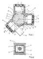
- FIG. 1 there is shown apparatus for the coating of a plurality of substrates 2.
- the substrates 2 are mounted on a substrate carrier 4 which in turn is mounted for rotation in a vacuum chamber 6.
- the chamber is provided with two material depositing means 8 mounted on the side walls of the chamber and facing inwardly toward the substrate carrier 4 for the deposition of material onto the substrates 2.
- the material is deposited by the sputtering of material from a target of the desired material mounted in the depositing means onto the substrates 2 to coat the same.
- both of the material depositing means 8 are operated by alternating voltage power supply and each material depositing means 8 is split and includes two magnetrons 7,7' which are arranged side by side and, at any one instant during operation, one is powered by the alternating voltage power supply to operate under a positive bias and the other is arranged to operate under a negative bias; the biases are periodically and synchronously changed in polarity by the alternating voltage power supply.
- the reaction producing means 9 includes a plasma source in the form, in this embodiment, of an unbalanced magnetron arrangement which is also driven by an alternating voltage power supply control and the arrangement comprises two side by side unbalanced magnetrons 11, 11' which are arranged to operate under positive and negative bias respectively.
- a plasma source in the form, in this embodiment, of an unbalanced magnetron arrangement which is also driven by an alternating voltage power supply control and the arrangement comprises two side by side unbalanced magnetrons 11, 11' which are arranged to operate under positive and negative bias respectively.
- a desired gas such as oxygen
- one of the magnetrons in the reaction producing means 11,11' or material depositing means 7,7' may be replaced by a counter electrode such that one cycle of the alternating voltage power supply powers the magnetron in the means and the other half cycle is received by the counter electrode thus allowing the same coating effect and advantages to be obtained with only one magnetron in the means.
- the substrate carrier 4 is, in this embodiment, substantially in the form of a cube and the substrates 2 are mounted on the vertical faces 10 of the same.
- the carrier in this embodiment, is also provided with four corner edges and these edges form gas partitioning vanes 12.
- the substrate carrier 4 is mounted for rotation about its central vertical axis and the chamber 6 is constructed such that the vanes, as the carrier 4 rotates, pass in close proximity to the walls of the chamber 6 thus preventing the easy flow of gases between the zones.
- the vacuum chamber 6 is also provided with a vacuum pump 14 connected thereto to cause the chamber to be under vacuum during use.
- FIG. 2 there is shown a sectional view into the vacuum chamber 6 on line A-A showing the substrate carrier 4 with a substrate 2 mounted thereon.
- the carrier 4 is mounted for rotation about the central axis 16 by a drive means (not shown) and, as it does so, the vanes 12 rotate in close proximity to the walls of the vacuum chamber 6.
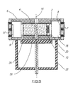
- Figure 3 illustrates a sectional elevation through the apparatus and shows the carrier 4, the vacuum chamber 6, one of the material depositing means 8 and the reaction means 9.
- the carrier 4 is shown carrying a substrate 2 on each of the sides 10.
- the material depositing means 8 is mounted in an area 18 of the chamber 6 and there is defined an aperture 20 which allows the material sputtered from the magnetrons 7,7' to pass onto the substrates 2 on the carrier 4 and the shape of the aperture 20 can be used to define the shape and pattern of sputtered material deposited.
- a loading chamber 32 which is shown below the vacuum chamber 6 in Figure 3.
- the loading chamber 32 and vacuum chamber are interconnected via an aperture 34 which is selectively openable by operation of a sealing plate 36.
- the provision of this chamber is to allow the carrier 4 with substrates 2 mounted thereon to be loaded and unloaded from the vacuum chamber whilst maintaining the vacuum in the vacuum chamber and thereby preventing damage to the reaction and material depositing means situated therein.
Landscapes
- Chemical & Material Sciences (AREA)
- Organic Chemistry (AREA)
- Engineering & Computer Science (AREA)
- Materials Engineering (AREA)
- Mechanical Engineering (AREA)
- Metallurgy (AREA)
- Chemical Kinetics & Catalysis (AREA)
- Physical Vapour Deposition (AREA)
- Crystals, And After-Treatments Of Crystals (AREA)
- Liquid Deposition Of Substances Of Which Semiconductor Devices Are Composed (AREA)
- Coating Apparatus (AREA)
- Optical Integrated Circuits (AREA)
- Liquid Crystal (AREA)
Abstract
Description
Claims (21)
- Apparatus for the deposition of material onto at least one substrate to form a coating, said apparatus comprising a vacuum chamber, a vacuum creating means, at least a first material deposition means, at least a first reaction producing means, a means for introducing gas or gases into the chamber and a substrate carrier mounted for rotation in the vacuum chamber and characterised in that at least one of the material deposition means and/or reaction means comprises at least one magnetron and a further magnetron or a counter electrode which are powered by an alternating voltage power supply such that at any one instant during operation one operates with a negative bias and the other operates with a positive bias.
- Apparatus according to claim 1 characterised in that the magnetrons of each material deposition means include targets of an appropriate material to be sputtered onto the substrates.
- Apparatus according to claim 1 characterised in that the magnetrons are mounted in a substantially vertical or horizontal plane in the vacuum chamber and facing inwardly toward the substrate carrier.
- Apparatus according to any of claims 1-3 characterised in that the magnetrons, or magnetron and its counter electrode, in the reaction producing means and/or material depositing means are arranged side by side.
- Apparatus according to claim 1 characterised in that the material depositing means comprises two magnetrons and at any one instant during operation, one is operated with a positive bias and the other with a negative bias.
- Apparatus according to claim 5 characterised in that the positive and negative biases between magnetrons can be periodically and synchronously exchanged.
- Apparatus according to claim 1 characterised in that the reaction producing means is a plasma source comprising two unbalanced magnetrons arranged side by side.
- Apparatus according to claim 7 characterised in that one unbalanced magnetron is operated with a positive bias and the other is operated with a negative bias at any one instant of operation and the biases can be periodically and synchronously changed between magnetrons during operation.
- Apparatus according to claim 1 characterised in that the reaction producing means is a plasma source comprising an unbalanced magnetron and a counter electrode arranged side by side.
- Apparatus according to claim 9 characterised in that either of the unbalanced magnetron and the counter electrode is operated with a positive bias and the other is operated with a negative bias at any one instant of operation and the biases can be periodically and synchronously changed during operation.
- Apparatus according to claim 1 characterised in that the reaction producing means is operated in a gas or a mixture of gases.
- Apparatus according to claim 11 characterised in that the gases are any of oxygen, hydrogen, nitrogen or methane gas.
- Apparatus according to claim 11 characterised in that the reaction producing means is operated in a gas to produce a carbon containing compound coating on the substrates.
- Apparatus according to any preceding claim characterised in that the substrate carrier, with the substrates mounted thereon, can be loaded into the chamber via a loadlock device thereby maintaining the vacuum in the vacuum chamber and preventing the reaction producing means and the material depositing means from being exposed to atmospheric pressure.
- Apparatus according to claim 12 characterised in that the substrates are mounted on the carrier external of the vacuum chamber and passed from a loading chamber interconnected and selectively openable into the vacuum chamber.
- Apparatus according to any of the preceding claims characterised in that two material producing means are provided each for the deposition of different materials onto the substrates.
- Apparatus according to claim 1 characterised in that the alternating voltage power supply is operable at any frequency between 1kBz and 1MHz.
- Apparatus according to claim 15 characterised in that frequency of operation is between 30 -50kHz.
- Apparatus for the deposition of material onto at least one substrate to form a coating, said apparatus comprising a vacuum chamber, a vacuum creating means, at least a first material deposition means, at least a first reaction producing means, a means for introducing gas or gases into the chamber and a substrate carrier mounted for rotation in the vacuum chamber and characterised in that alternating current is used to power any or any combination of the material depositing means and/or reaction producing means.
- Apparatus according to claim 19 characterised in that one material depositing means and a reaction producing means are powered by alternating current and, a first, half cycle of each cycle of the power supply is used to power the material depositing means and the second half cycle is used to power the reaction producing means.
- Apparatus according to claim 19 characterised in that two material depositing means are powered by alternating current and the power supply half cycle is switched between first and second material depositing means as required to provide the required activation of the depositing means to produce multilayered materials coatings on the substrates.
Applications Claiming Priority (3)
| Application Number | Priority Date | Filing Date | Title |
|---|---|---|---|
| GB9405442 | 1994-03-19 | ||
| GB9405442A GB9405442D0 (en) | 1994-03-19 | 1994-03-19 | Apparatus for coating substrates |
| PCT/GB1995/000607 WO1995025828A1 (en) | 1994-03-19 | 1995-03-20 | Apparatus for coating substrates |
Publications (2)
| Publication Number | Publication Date |
|---|---|
| EP0699246A1 EP0699246A1 (en) | 1996-03-06 |
| EP0699246B1 true EP0699246B1 (en) | 1999-01-07 |
Family
ID=10752161
Family Applications (2)
| Application Number | Title | Priority Date | Filing Date |
|---|---|---|---|
| EP95911413A Expired - Lifetime EP0699245B1 (en) | 1994-03-19 | 1995-03-17 | Process for coating substrates |
| EP95911438A Revoked EP0699246B1 (en) | 1994-03-19 | 1995-03-20 | Apparatus for coating substrates |
Family Applications Before (1)
| Application Number | Title | Priority Date | Filing Date |
|---|---|---|---|
| EP95911413A Expired - Lifetime EP0699245B1 (en) | 1994-03-19 | 1995-03-17 | Process for coating substrates |
Country Status (7)
| Country | Link |
|---|---|
| US (2) | US6090248A (en) |
| EP (2) | EP0699245B1 (en) |
| AT (2) | ATE209262T1 (en) |
| AU (2) | AU1898995A (en) |
| DE (2) | DE69524009T2 (en) |
| GB (1) | GB9405442D0 (en) |
| WO (2) | WO1995025827A2 (en) |
Cited By (1)
| Publication number | Priority date | Publication date | Assignee | Title |
|---|---|---|---|---|
| DE10311466B4 (en) * | 2003-03-15 | 2005-07-21 | Fraunhofer-Gesellschaft zur Förderung der angewandten Forschung e.V. | Method for reactive magnetron sputtering |
Families Citing this family (19)
| Publication number | Priority date | Publication date | Assignee | Title |
|---|---|---|---|---|
| DE19609804C1 (en) * | 1996-03-13 | 1997-07-31 | Bosch Gmbh Robert | Device, its use and its operation for vacuum coating of bulk goods |
| DE19738234C1 (en) * | 1997-09-02 | 1998-10-22 | Fraunhofer Ges Forschung | Apparatus for producing sputtered coatings consisting of hard substances |
| DE19834314A1 (en) * | 1998-07-30 | 2000-02-03 | Leybold Systems Gmbh | Application of a scratch resistant coating and an antireflective system onto a plastic substrate, in particular spectacle lenses by consecutive plasma and sputtering methods |
| US6527866B1 (en) * | 2000-02-09 | 2003-03-04 | Conductus, Inc. | Apparatus and method for deposition of thin films |
| US6429097B1 (en) * | 2000-05-22 | 2002-08-06 | Sharp Laboratories Of America, Inc. | Method to sputter silicon films |
| EP1275751A1 (en) * | 2001-07-13 | 2003-01-15 | Satis Vacuum Industries Vertriebs - AG | Process and apparatus for producing an optically active coating system |
| WO2005035822A1 (en) * | 2003-10-07 | 2005-04-21 | Deposition Sciences, Inc. | Apparatus and process for high rate deposition of rutile titanium dioxide |
| US20050100665A1 (en) * | 2003-11-06 | 2005-05-12 | General Electric Company | Method for applying an optical coating to a surface of an article |
| US20060236931A1 (en) * | 2005-04-25 | 2006-10-26 | Varian Semiconductor Equipment Associates, Inc. | Tilted Plasma Doping |
| US20070173925A1 (en) * | 2006-01-25 | 2007-07-26 | Cornova, Inc. | Flexible expandable stent |
| US20080215132A1 (en) * | 2006-08-28 | 2008-09-04 | Cornova, Inc. | Implantable devices having textured surfaces and methods of forming the same |
| US7892598B1 (en) * | 2006-12-19 | 2011-02-22 | Intelli-Plac LLC | Method of providing a reusable labeling surface for receiving a removable element on the surface of an object |
| KR20090126863A (en) * | 2008-06-05 | 2009-12-09 | 삼성전자주식회사 | Method for forming multilayer encapsulation thin film having optical functionality and multilayer encapsulation thin film manufactured thereby |
| DE102008062332A1 (en) * | 2008-12-15 | 2010-06-17 | Gühring Ohg | Device for surface treatment and / or coating of substrate components |
| EP2718959B1 (en) | 2011-06-07 | 2018-10-31 | Vision Ease LP | Improvements to the application of coating materials |
| JP5713872B2 (en) * | 2011-10-28 | 2015-05-07 | 株式会社神戸製鋼所 | Film forming apparatus and film forming method |
| CN103160792B (en) * | 2011-12-12 | 2017-02-08 | 许聪波 | Coating device |
| EP3794157B1 (en) * | 2018-05-17 | 2022-03-16 | Evatec AG | Method of treating a substrate and vacuum deposition apparatus |
| US12331400B2 (en) * | 2022-11-07 | 2025-06-17 | Creating Nano Technologies, Inc. | Surface treatment apparatus |
Family Cites Families (12)
| Publication number | Priority date | Publication date | Assignee | Title |
|---|---|---|---|---|
| LU52106A1 (en) * | 1966-10-05 | 1968-05-07 | ||
| US3641973A (en) * | 1970-11-25 | 1972-02-15 | Air Reduction | Vacuum coating apparatus |
| JPS6039162A (en) * | 1983-08-10 | 1985-02-28 | Anelva Corp | Vacuum apparatus for treating thin film |
| GB8413776D0 (en) * | 1984-05-30 | 1984-07-04 | Dowty Electronics Ltd | Sputtering process |
| US4724296A (en) * | 1986-02-28 | 1988-02-09 | Morley John R | Plasma generator |
| US4851095A (en) * | 1988-02-08 | 1989-07-25 | Optical Coating Laboratory, Inc. | Magnetron sputtering apparatus and process |
| EP0529687B1 (en) * | 1988-03-30 | 1996-05-29 | Rohm Co., Ltd. | Molecular beam epitaxy apparatus |
| GB9006073D0 (en) * | 1990-03-17 | 1990-05-16 | D G Teer Coating Services Limi | Magnetron sputter ion plating |
| GB9101106D0 (en) * | 1991-01-18 | 1991-02-27 | Cray Microcoat Ltd | Ion vapour deposition apparatus and method |
| DE4106770C2 (en) * | 1991-03-04 | 1996-10-17 | Leybold Ag | Performing reactive coating of a substrate |
| DE59202577D1 (en) * | 1991-03-05 | 1995-07-27 | Balzers Hochvakuum | Process for producing a double-sided coating of optical workpieces. |
| US5415757A (en) * | 1991-11-26 | 1995-05-16 | Leybold Aktiengesellschaft | Apparatus for coating a substrate with electrically nonconductive coatings |
-
1994
- 1994-03-19 GB GB9405442A patent/GB9405442D0/en active Pending
-
1995
- 1995-03-17 AT AT95911413T patent/ATE209262T1/en not_active IP Right Cessation
- 1995-03-17 DE DE69524009T patent/DE69524009T2/en not_active Expired - Lifetime
- 1995-03-17 EP EP95911413A patent/EP0699245B1/en not_active Expired - Lifetime
- 1995-03-17 AU AU18989/95A patent/AU1898995A/en not_active Abandoned
- 1995-03-17 US US08/553,444 patent/US6090248A/en not_active Expired - Lifetime
- 1995-03-17 WO PCT/GB1995/000580 patent/WO1995025827A2/en not_active Ceased
- 1995-03-20 DE DE69507095T patent/DE69507095T2/en not_active Expired - Fee Related
- 1995-03-20 WO PCT/GB1995/000607 patent/WO1995025828A1/en not_active Ceased
- 1995-03-20 US US08/549,857 patent/US6090247A/en not_active Expired - Lifetime
- 1995-03-20 AT AT95911438T patent/ATE175451T1/en not_active IP Right Cessation
- 1995-03-20 AU AU19009/95A patent/AU1900995A/en not_active Abandoned
- 1995-03-20 EP EP95911438A patent/EP0699246B1/en not_active Revoked
Cited By (1)
| Publication number | Priority date | Publication date | Assignee | Title |
|---|---|---|---|---|
| DE10311466B4 (en) * | 2003-03-15 | 2005-07-21 | Fraunhofer-Gesellschaft zur Förderung der angewandten Forschung e.V. | Method for reactive magnetron sputtering |
Also Published As
| Publication number | Publication date |
|---|---|
| US6090248A (en) | 2000-07-18 |
| EP0699246A1 (en) | 1996-03-06 |
| DE69507095D1 (en) | 1999-02-18 |
| DE69524009D1 (en) | 2002-01-03 |
| AU1898995A (en) | 1995-10-09 |
| DE69524009T2 (en) | 2002-07-11 |
| WO1995025827A2 (en) | 1995-09-28 |
| EP0699245A1 (en) | 1996-03-06 |
| WO1995025827A3 (en) | 1995-10-12 |
| WO1995025828A1 (en) | 1995-09-28 |
| GB9405442D0 (en) | 1994-05-04 |
| DE69507095T2 (en) | 1999-07-15 |
| AU1900995A (en) | 1995-10-09 |
| ATE209262T1 (en) | 2001-12-15 |
| US6090247A (en) | 2000-07-18 |
| EP0699245B1 (en) | 2001-11-21 |
| ATE175451T1 (en) | 1999-01-15 |
Similar Documents
| Publication | Publication Date | Title |
|---|---|---|
| US6090247A (en) | Apparatus for coating substrates | |
| US6113752A (en) | Method and device for coating substrate | |
| CA2110250C (en) | Depositing different materials on a substrate | |
| WO2006038407A2 (en) | Vacuum film forming apparatus | |
| TW201700760A (en) | Ring cathode applied to magnetron sputtering device | |
| AU692332B2 (en) | Process and apparatus for forming thin films of metallic compounds | |
| KR101050983B1 (en) | Thin film forming apparatus and thin film forming method | |
| US5690796A (en) | Method and apparatus for layer depositions | |
| JP4005172B2 (en) | Double-sided simultaneous film formation method and apparatus | |
| JP3293912B2 (en) | Method of forming oxide thin film | |
| JP3773320B2 (en) | Film forming apparatus and film forming method | |
| WO1992013114A1 (en) | Ion vapour deposition apparatus and method | |
| JP4137611B2 (en) | Method for forming laminated film | |
| JP2007507618A5 (en) | ||
| JPS61210190A (en) | Thin film forming device | |
| JPH04346655A (en) | Method and device for forming compound thin film | |
| JPH10287973A (en) | Sputtering device | |
| JPH02240261A (en) | Sputtering device | |
| JPH06330303A (en) | Device for forming thin film | |
| JP2003213408A (en) | Reactive sputtering method, and film deposition apparatus therefor | |
| JP2020045510A (en) | Vacuum processing equipment | |
| JPH069246A (en) | Method for forming film of oxide thin film | |
| JP2905421B2 (en) | Reactive sputtering equipment | |
| JPS6376867A (en) | Reactive sputtering equipment | |
| JPH01156465A (en) | Sputtering device |
Legal Events
| Date | Code | Title | Description |
|---|---|---|---|
| PUAI | Public reference made under article 153(3) epc to a published international application that has entered the european phase |
Free format text: ORIGINAL CODE: 0009012 |
|
| 17P | Request for examination filed |
Effective date: 19951118 |
|
| AK | Designated contracting states |
Kind code of ref document: A1 Designated state(s): AT BE CH DE DK ES FR GB GR IE IT LI LU MC NL PT SE |
|
| GRAG | Despatch of communication of intention to grant |
Free format text: ORIGINAL CODE: EPIDOS AGRA |
|
| 17Q | First examination report despatched |
Effective date: 19980318 |
|
| GRAG | Despatch of communication of intention to grant |
Free format text: ORIGINAL CODE: EPIDOS AGRA |
|
| GRAH | Despatch of communication of intention to grant a patent |
Free format text: ORIGINAL CODE: EPIDOS IGRA |
|
| GRAH | Despatch of communication of intention to grant a patent |
Free format text: ORIGINAL CODE: EPIDOS IGRA |
|
| GRAA | (expected) grant |
Free format text: ORIGINAL CODE: 0009210 |
|
| AK | Designated contracting states |
Kind code of ref document: B1 Designated state(s): AT BE CH DE DK ES FR GB GR IE IT LI LU MC NL PT SE |
|
| PG25 | Lapsed in a contracting state [announced via postgrant information from national office to epo] |
Ref country code: SE Free format text: LAPSE BECAUSE OF FAILURE TO SUBMIT A TRANSLATION OF THE DESCRIPTION OR TO PAY THE FEE WITHIN THE PRESCRIBED TIME-LIMIT Effective date: 19990107 Ref country code: NL Free format text: LAPSE BECAUSE OF FAILURE TO SUBMIT A TRANSLATION OF THE DESCRIPTION OR TO PAY THE FEE WITHIN THE PRESCRIBED TIME-LIMIT Effective date: 19990107 Ref country code: GR Free format text: LAPSE BECAUSE OF NON-PAYMENT OF DUE FEES Effective date: 19990107 Ref country code: BE Free format text: LAPSE BECAUSE OF FAILURE TO SUBMIT A TRANSLATION OF THE DESCRIPTION OR TO PAY THE FEE WITHIN THE PRESCRIBED TIME-LIMIT Effective date: 19990107 Ref country code: AT Free format text: LAPSE BECAUSE OF FAILURE TO SUBMIT A TRANSLATION OF THE DESCRIPTION OR TO PAY THE FEE WITHIN THE PRESCRIBED TIME-LIMIT Effective date: 19990107 |
|
| REF | Corresponds to: |
Ref document number: 175451 Country of ref document: AT Date of ref document: 19990115 Kind code of ref document: T |
|
| REG | Reference to a national code |
Ref country code: CH Ref legal event code: EP |
|
| ITF | It: translation for a ep patent filed | ||
| REF | Corresponds to: |
Ref document number: 69507095 Country of ref document: DE Date of ref document: 19990218 |
|
| REG | Reference to a national code |
Ref country code: IE Ref legal event code: FG4D |
|
| REG | Reference to a national code |
Ref country code: CH Ref legal event code: NV Representative=s name: ABREMA AGENCE BREVETS ET MARQUES GANGUILLET & HUMP |
|
| ET | Fr: translation filed | ||
| PG25 | Lapsed in a contracting state [announced via postgrant information from national office to epo] |
Ref country code: LU Free format text: LAPSE BECAUSE OF NON-PAYMENT OF DUE FEES Effective date: 19990320 Ref country code: IE Free format text: LAPSE BECAUSE OF NON-PAYMENT OF DUE FEES Effective date: 19990320 |
|
| PG25 | Lapsed in a contracting state [announced via postgrant information from national office to epo] |
Ref country code: PT Free format text: LAPSE BECAUSE OF FAILURE TO SUBMIT A TRANSLATION OF THE DESCRIPTION OR TO PAY THE FEE WITHIN THE PRESCRIBED TIME-LIMIT Effective date: 19990407 Ref country code: DK Free format text: LAPSE BECAUSE OF FAILURE TO SUBMIT A TRANSLATION OF THE DESCRIPTION OR TO PAY THE FEE WITHIN THE PRESCRIBED TIME-LIMIT Effective date: 19990407 |
|
| PG25 | Lapsed in a contracting state [announced via postgrant information from national office to epo] |
Ref country code: ES Free format text: LAPSE BECAUSE OF FAILURE TO SUBMIT A TRANSLATION OF THE DESCRIPTION OR TO PAY THE FEE WITHIN THE PRESCRIBED TIME-LIMIT Effective date: 19990408 |
|
| NLV1 | Nl: lapsed or annulled due to failure to fulfill the requirements of art. 29p and 29m of the patents act | ||
| PG25 | Lapsed in a contracting state [announced via postgrant information from national office to epo] |
Ref country code: MC Free format text: LAPSE BECAUSE OF NON-PAYMENT OF DUE FEES Effective date: 19990930 |
|
| PLBQ | Unpublished change to opponent data |
Free format text: ORIGINAL CODE: EPIDOS OPPO |
|
| PLBQ | Unpublished change to opponent data |
Free format text: ORIGINAL CODE: EPIDOS OPPO |
|
| PLBI | Opposition filed |
Free format text: ORIGINAL CODE: 0009260 |
|
| 26 | Opposition filed |
Opponent name: LEYBOLD AKTIENGESELLSCHAFT Effective date: 19991006 Opponent name: VON ARDENNE ANLAGENTECHNIK GMBH Effective date: 19991007 Opponent name: FRAUNHOFER-GESELLSCHAFT ZUR FOERDERUNG DER ANGEWAN Effective date: 19991006 |
|
| PLBF | Reply of patent proprietor to notice(s) of opposition |
Free format text: ORIGINAL CODE: EPIDOS OBSO |
|
| REG | Reference to a national code |
Ref country code: IE Ref legal event code: MM4A |
|
| PGFP | Annual fee paid to national office [announced via postgrant information from national office to epo] |
Ref country code: GB Payment date: 20000118 Year of fee payment: 6 |
|
| PGFP | Annual fee paid to national office [announced via postgrant information from national office to epo] |
Ref country code: FR Payment date: 20000324 Year of fee payment: 6 |
|
| PGFP | Annual fee paid to national office [announced via postgrant information from national office to epo] |
Ref country code: CH Payment date: 20000328 Year of fee payment: 6 |
|
| PLBF | Reply of patent proprietor to notice(s) of opposition |
Free format text: ORIGINAL CODE: EPIDOS OBSO |
|
| PGFP | Annual fee paid to national office [announced via postgrant information from national office to epo] |
Ref country code: DE Payment date: 20000518 Year of fee payment: 6 |
|
| PLBF | Reply of patent proprietor to notice(s) of opposition |
Free format text: ORIGINAL CODE: EPIDOS OBSO |
|
| PG25 | Lapsed in a contracting state [announced via postgrant information from national office to epo] |
Ref country code: GB Free format text: LAPSE BECAUSE OF NON-PAYMENT OF DUE FEES Effective date: 20010320 |
|
| PG25 | Lapsed in a contracting state [announced via postgrant information from national office to epo] |
Ref country code: LI Free format text: LAPSE BECAUSE OF NON-PAYMENT OF DUE FEES Effective date: 20010331 Ref country code: CH Free format text: LAPSE BECAUSE OF NON-PAYMENT OF DUE FEES Effective date: 20010331 |
|
| PLBQ | Unpublished change to opponent data |
Free format text: ORIGINAL CODE: EPIDOS OPPO |
|
| PLAB | Opposition data, opponent's data or that of the opponent's representative modified |
Free format text: ORIGINAL CODE: 0009299OPPO |
|
| PLAB | Opposition data, opponent's data or that of the opponent's representative modified |
Free format text: ORIGINAL CODE: 0009299OPPO |
|
| R26 | Opposition filed (corrected) |
Opponent name: FRAUNHOFER-GESELLSCHAFT ZUR FOERDERUNG DER ANGEWAN Effective date: 19991006 |
|
| GBPC | Gb: european patent ceased through non-payment of renewal fee |
Effective date: 20010320 |
|
| R26 | Opposition filed (corrected) |
Opponent name: FRAUNHOFER-GESELLSCHAFT ZUR FOERDERUNG DER ANGEWAN Effective date: 19991006 |
|
| REG | Reference to a national code |
Ref country code: CH Ref legal event code: PL |
|
| RDAH | Patent revoked |
Free format text: ORIGINAL CODE: EPIDOS REVO |
|
| PG25 | Lapsed in a contracting state [announced via postgrant information from national office to epo] |
Ref country code: FR Free format text: LAPSE BECAUSE OF NON-PAYMENT OF DUE FEES Effective date: 20011130 |
|
| REG | Reference to a national code |
Ref country code: FR Ref legal event code: ST |
|
| RDAG | Patent revoked |
Free format text: ORIGINAL CODE: 0009271 |
|
| STAA | Information on the status of an ep patent application or granted ep patent |
Free format text: STATUS: PATENT REVOKED |
|
| 27W | Patent revoked |
Effective date: 20011206 |