EP0691643B1 - Dispositif de commande électrique à correction de diaphonie et application à des têtes magnétiques d'enregistrement/lecture - Google Patents
Dispositif de commande électrique à correction de diaphonie et application à des têtes magnétiques d'enregistrement/lecture Download PDFInfo
- Publication number
- EP0691643B1 EP0691643B1 EP95401526A EP95401526A EP0691643B1 EP 0691643 B1 EP0691643 B1 EP 0691643B1 EP 95401526 A EP95401526 A EP 95401526A EP 95401526 A EP95401526 A EP 95401526A EP 0691643 B1 EP0691643 B1 EP 0691643B1
- Authority
- EP
- European Patent Office
- Prior art keywords
- resistive
- limiting
- elements
- layer
- coupling
- Prior art date
- Legal status (The legal status is an assumption and is not a legal conclusion. Google has not performed a legal analysis and makes no representation as to the accuracy of the status listed.)
- Expired - Lifetime
Links
- 230000008878 coupling Effects 0.000 claims description 31
- 238000010168 coupling process Methods 0.000 claims description 31
- 238000005859 coupling reaction Methods 0.000 claims description 31
- 239000003990 capacitor Substances 0.000 claims description 10
- 239000011159 matrix material Substances 0.000 claims description 10
- 239000000758 substrate Substances 0.000 claims description 8
- 239000003989 dielectric material Substances 0.000 claims description 7
- 239000004020 conductor Substances 0.000 claims 7
- 230000001747 exhibiting effect Effects 0.000 claims 1
- 238000004804 winding Methods 0.000 description 21
- 238000001465 metallisation Methods 0.000 description 10
- 230000000875 corresponding effect Effects 0.000 description 3
- 235000021183 entrée Nutrition 0.000 description 2
- 238000004519 manufacturing process Methods 0.000 description 2
- 238000000034 method Methods 0.000 description 2
- 238000002679 ablation Methods 0.000 description 1
- 230000000996 additive effect Effects 0.000 description 1
- 230000002596 correlated effect Effects 0.000 description 1
- 230000001627 detrimental effect Effects 0.000 description 1
- 238000010586 diagram Methods 0.000 description 1
- 230000001939 inductive effect Effects 0.000 description 1
- 238000009413 insulation Methods 0.000 description 1
- 230000010354 integration Effects 0.000 description 1
- 230000003287 optical effect Effects 0.000 description 1
- 244000045947 parasite Species 0.000 description 1
- 238000004513 sizing Methods 0.000 description 1
Images


Classifications
-
- G—PHYSICS
- G11—INFORMATION STORAGE
- G11B—INFORMATION STORAGE BASED ON RELATIVE MOVEMENT BETWEEN RECORD CARRIER AND TRANSDUCER
- G11B20/00—Signal processing not specific to the method of recording or reproducing; Circuits therefor
- G11B20/10—Digital recording or reproducing
- G11B20/18—Error detection or correction; Testing, e.g. of drop-outs
-
- G—PHYSICS
- G11—INFORMATION STORAGE
- G11B—INFORMATION STORAGE BASED ON RELATIVE MOVEMENT BETWEEN RECORD CARRIER AND TRANSDUCER
- G11B5/00—Recording by magnetisation or demagnetisation of a record carrier; Reproducing by magnetic means; Record carriers therefor
- G11B5/127—Structure or manufacture of heads, e.g. inductive
- G11B5/29—Structure or manufacture of unitary devices formed of plural heads for more than one track
-
- G—PHYSICS
- G11—INFORMATION STORAGE
- G11B—INFORMATION STORAGE BASED ON RELATIVE MOVEMENT BETWEEN RECORD CARRIER AND TRANSDUCER
- G11B23/00—Record carriers not specific to the method of recording or reproducing; Accessories, e.g. containers, specially adapted for co-operation with the recording or reproducing apparatus ; Intermediate mediums; Apparatus or processes specially adapted for their manufacture
- G11B23/0007—Circuits or methods for reducing noise, for correction of distortion, or for changing density of recorded information
-
- G—PHYSICS
- G11—INFORMATION STORAGE
- G11B—INFORMATION STORAGE BASED ON RELATIVE MOVEMENT BETWEEN RECORD CARRIER AND TRANSDUCER
- G11B5/00—Recording by magnetisation or demagnetisation of a record carrier; Reproducing by magnetic means; Record carriers therefor
- G11B5/48—Disposition or mounting of heads or head supports relative to record carriers ; arrangements of heads, e.g. for scanning the record carrier to increase the relative speed
- G11B5/4806—Disposition or mounting of heads or head supports relative to record carriers ; arrangements of heads, e.g. for scanning the record carrier to increase the relative speed specially adapted for disk drive assemblies, e.g. assembly prior to operation, hard or flexible disk drives
- G11B5/484—Integrated arm assemblies, e.g. formed by material deposition or by etching from single piece of metal or by lamination of materials forming a single arm/suspension/head unit
-
- G—PHYSICS
- G11—INFORMATION STORAGE
- G11B—INFORMATION STORAGE BASED ON RELATIVE MOVEMENT BETWEEN RECORD CARRIER AND TRANSDUCER
- G11B5/00—Recording by magnetisation or demagnetisation of a record carrier; Reproducing by magnetic means; Record carriers therefor
- G11B5/48—Disposition or mounting of heads or head supports relative to record carriers ; arrangements of heads, e.g. for scanning the record carrier to increase the relative speed
- G11B5/49—Fixed mounting or arrangements, e.g. one head per track
- G11B5/4969—Details for track selection or addressing
Definitions
- the invention relates to an electrical control device with crosstalk correction and its application to magnetic heads recording / playback.
- a source or a matrix of devices electrically controllable such as electromagnetic devices (magnetic heads for example) or optical devices for compensate for crosstalk that may exist between neighboring devices.
- the invention consists of a physical and passive device associated with a arrangement of elements allowing electrically to compensate for crosstalk magnetic that exists in the multi-track writing component on media magnetic.
- This device replaces a set of passive components - resistors and capacities associated with their connections - arranged between the writing current generation electronics and the windings of the writing component.
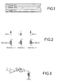
- the invention applies in the context of a system recording and reading of data on magnetic media, where the format physical data writing to tape is of the multi-track type in parallel, as shown in Figure 1.
- Magnetic crosstalk in writing is manifested by a partial writing of data normally intended for a J track on the neighboring tracks D-1 and D + 1.
- a multi-track magnetic recorder has a large number of magnetic heads (1024 for example) allows to write 1024 tracks on a 12.54 mm high strip.
- Such a device has a matrix structure; the 1024 magnetic air gaps are distributed over a parallelogram 16 columns long and 64 rows of high.
- this parallelogram - essentially the angle- is judiciously chosen to write 1024 tracks on the magnetic strip adjacent and without overlap between tracks.
- Each column and each line has an addressed winding electrically.
- the currents flowing through columns and rows do not generate enough field for writing on strip at the location of the corresponding air gaps.
- the additive action of the currents allows to generate in the corresponding air gap a sufficient field for writing data to tape.
- Bd kd x B, where kd represents the cross-talk coefficient between columns of the writing head.
- Figure 3 illustrates the electrical assembly used.
- the capacity C of low value, is intended to increase the current rise time in the windings.
- the common point of the windings set to + V / 2 allows creating currents + I and -I from a single voltage.
- French Patent Application No. FR-A-2 699 722 describes a device providing coupling resistors to compensate for the crosstalk, as defined in the preamble of claim 1.
- Crosstalk correction resistors, Rd derive part kd of the current from J to J-1 and J + 1, and give birth to the magnetic field which cancels the stray field.
- the writing component requires a network of 288 resistors to work properly.
- the object of the invention is to simplify the design and implementation crosstalk correction circuits and even reduce the number of resistances required.
- the invention therefore relates to an electrical control device with crosstalk correction for magnetic recording / reading heads, comprising several controllable devices electrically each by a limiting resistor, and by elements resistive coupling, each resistive coupling element coupling a limiting resistance to a neighboring limiting resistance, characterized in what the current limiting resistors are resistive elements of limitation in planar layers arranged on a first face of substrate and in that the resistive coupling elements are also produced in flat layers and are arranged transversely to the resistive elements of limitation and interconnecting these resistive limiting elements
- the invention is applicable to the control of a matrix head recording / playback.
- the device proposed to replace all of the resistors current limiting and crosstalk is a resistive surface with an anisotropy of resistivity along its X and Y axes. This anisotropy is obtained either by a form factor of the device, or by a choice of patterns resistives that cross at 90 degrees.
- FIG. 7 represents the structure in the configuration called in bridge.
- the electromagnetic devices to be controlled are represented by the windings B1 to B5. As can be seen by the signs "+” and “-” associated with their accesses, these windings have alternating winding directions as explained in relation to FIGS. 5 and 6. Circuits of control send at low impedance the voltages + V and 0 on each network inputs: the length "a" dimensions the resistance ⁇ 2 which realize the current limitation i1 in each winding, of impedance Z very small, while the distance between studs "b” determines the proportion id of the main current which is diverted to the neighboring windings.
- This structure performs analog mixing of current, inter-windings.
- the 288 resistors are replaced by 3 "resistive mixers"; 1 for the set of the 64 lines, and 2 for the 16 columns which are addressed in bridge.
- the ratio of dimensions (a: b) which determines the kd of the device can lead to a sizing of the assembly incompatible with the environment of the component.
- a structure is made up of two resistive layers in cross contact each consisting of strips parallels of different resistances, as shown in figure 8.
- the geometric design of the device is then independent of its electrical characteristics.
- Elements such as ⁇ 1 represent resistive elements of current limitation connecting each electromagnetic device B1 to Bn to be ordered at the control circuits.
- the element such as ⁇ 2 represented perpendicular to ⁇ 1 is a resistive coupling element in electrical contact with each element current limiting resistive ⁇ 1.
- the resistive elements ⁇ 1 are made in thin or thick layer on a substrate plate.
- the ⁇ 2 elements are also produced in a thin or thick layer on the ⁇ 1 elements and on the substrate plate.
- the calibration of dimensions in thickness and in particular in width allows to adjust the resistance values.
- the number of elements ⁇ 2 makes it possible to adjust the coupling.
- the resistive coupling element can be pre-formed, as represented in figure 9 to take into account a characteristic constant of the component to be corrected.
- the element ⁇ 2 has a shape adapted to the couplings to be carried out.
- there slots are provided in the ⁇ 2 element to adjust the couplings as desired resistive between elements ⁇ 1.
- the device can be adjusted by laser, and this at the level of each winding, by partial ablation of the layers resistive for adjustment of main current and correction currents crosstalk.
- FIGs 10a and 10b show an alternative embodiment of the invention in which resistive elements such as ⁇ 2 and ⁇ '2 are provided connecting the access of each resistive element ⁇ 1 on the circuit side of control on the winding side access of the resistive elements immediately neighbors.
- resistive elements such as ⁇ 2 and ⁇ '2 are provided connecting the access of each resistive element ⁇ 1 on the circuit side of control on the winding side access of the resistive elements immediately neighbors.
- a resistive coupling between input and output is thus obtained as is shown in Figures 5 and 6.
- Figure 10b shows a sectional view which highlights that the resistive elements ⁇ 2 and ⁇ '2 are isolated from each other by a layer insulation I1.
- the section in figure 11 shows a type of embodiment allowing this component to be integrated into the device.
- the capacitive coupling is carried out by two layers of metallization opposite. This device is reproduced for each order winding.
- FIG. 11 is a simplified representation of such a mode of production. It is applied to the device of FIG. 8 comprising several resistive coupling elements ⁇ 2.
- This device comprises on the back of the ⁇ 1 element, a first metallization M1 connected to one end of the element ⁇ 1 and a second metallization M2 connected to the other end of the element ⁇ 1. Between the two metallizations is provided a dielectric material C1.
- the resistive elements ⁇ 1 and ⁇ 2 can be produced on one face of a substrate and the capacitors constituted by metallizations M1, M2 and the dielectric C1 can be made on the opposite side of the substrate.
- FIG. 12 represents a device according to the invention in which coupling capacitors are provided between the inputs of the elements ⁇ 1 resistors and the outputs of neighboring resistive elements.
- the resistive coupling elements ⁇ 2 have not been shown.
- Each metallization M1 associated with a resistive element ⁇ 1 has a conductive tab L1, L'1 on each side of the metallization which extends towards the metallization M1 of the neighboring resistive element.
- Each tab L1, L'1 of a resistive element is located above an N1 or N'1 tab of a neighboring resistive element and the two tabs are separated by a dielectric material so as to form a capacitor. Capacitors are thus produced in parallel with the resistive coupling elements ⁇ 2 whose value depends on the surface in look.
- Figure 13 shows an example of integration of the command described above with a matrix magnetic head produced in the form of a plate P.
- One face of the plate P1 has the poles of the magnetic heads and air gaps. This face therefore serves as an active face.
- the previously described control device produced in the form of a plate P2 is attached to the main face of the plate P1 opposite the face active.
- a matrix magnetic head can be produced as is described in French Patent Application No. 2,648,940 corresponding to EP-A-0.406.052 and we attach a plate P2 then the windings are to be connected to the circuits of the plate P2.
Landscapes
- Engineering & Computer Science (AREA)
- Manufacturing & Machinery (AREA)
- Signal Processing (AREA)
- Magnetic Heads (AREA)
- Signal Processing Not Specific To The Method Of Recording And Reproducing (AREA)
Description
B = k x I, où k représente l'efficacité de la tête d'écriture.
- 64 + 2x16 = 96 circuits de commande
- 64 + 2x16 = 96 résistances de contrôle du courant des bobinages
- 2x64 + 4x16 = 192 résistances de correction de diaphonie.
- un premier ensemble d'éléments résistifs de couplage connectant chacune une entrée d'un élément résistif de limitation de rang pair à une sortie d'un élément résistif de limitation voisin de rang impair ;
- un deuxième ensemble d'éléments résistifs isolés des premiers connectant chacun une sortie d'un élément résistif de limitation de rang pair à une entrée d'un élément résistif de limitation de rang impair.
- les figures 1 à 6, des dispositifs de commande électromagnétiques connus dans la technique ;
- la figure 7, un exemple général du dispositif de commande à correction de diaphonie selon l'invention ;
- la figure 8, un autre mode de réalisation du dispositif de commande selon l'invention ;
- la figure 9, une variante de réalisation du dispositif de la figure 8 ;
- les figures 10a et 10b, un mode de réalisation plus complexe du dispositif de commande selon l'invention ;
- la figure 11, un dispositif de commande comportant un condensateur en parallèle avec chaque élément résistif de limitation de courant ;
- la figure 12, un dispositif de commande comportant des condensateurs en parallèle avec les éléments résistifs de couplage ;
- la figure 13, un exemple d'application à une tête matricielle.
Claims (15)
- Dispositif de commande électrique à correction de diaphonie pour têtes magnétiques d'enregistrement/lecture, comprenant plusieurs dispositifs commandables électriquement chacun par une résistance de limitation (Ω1), et par des éléments résistifs de couplage (Ω2), chaque élément résistif de couplage couplant une résistance de limitation (Ω1) à une résistance de limitation voisine, caractérisé en ce que les résistances de limitation de courant (Ω1) sont des éléments résistifs de limitation en couches planes disposés sur une première face de substrat (S) et en ce que les éléments résistifs de couplage (Ω2) sont également réalisés en couches planes et sont disposés transversalement aux éléments résistifs de limitation et interconnectant ces éléments résistifs de limitation.
- Dispositif selon la revendication 1, caractérisé en ce que l'élément résistif de couplage (Ω2) présente une anisotropie de résistivité présentant un axe parallèle aux éléments résistifs de limitation.
- Dispositif selon la revendication 1, caractérisé en ce que les éléments résistifs de limitation (Ω1) sont parallèles entre eux.
- Dispositif selon la revendication 3, caractérisé en ce qu'il comporte un seul élément résistif de couplage (Ω2) qui est sensiblement perpendiculaire aux éléments résistifs de limitation.
- Dispositif selon la revendication 4, caractérisé en ce que l'élément résistif de couplage (Ω2) a une forme linéaire et de section constante.
- Dispositif selon la revendication 4, caractérisé en ce que l'élément résistif de couplage a une forme non linéaire et de section variable de façon à ce que la valeur de chaque élément résistif de couplage entre deux éléments résistifs de limitation puisse être adaptée.
- Dispositif selon la revendication 6, caractérisé en ce que l'élément résistif de couplage possède des encoches de réglage de valeur de résistance situées entre les éléments résistifs de limitation.
- Dispositif selon la revendication 3, caractérisé en ce qu'il comporteun premier ensemble d'éléments résistifs de couplage connectant chacune une entrée d'un élément résistif de limitation de rang pair à une sortie d'un élément résistif de limitation voisin de rang impair ;un deuxième ensemble d'éléments résistifs isolés des premiers connectant chacun une sortie d'un élément résistif de limitation de rang pair à une entrée d'un élément résistif voisin de limitation de rang impair.
- Dispositif de commande électrique à correction de diaphonie selon la revendication 1, caractérisé en ce qu'il comprend plusieurs dispositifs électromagnétiques commandables électriquement chacun par les résistances de limitation de courant (Ω1) qui sont disposées sur une première face d'un substrat (S) en ce qu'il comporte empilées sur une deuxième face du substrat (S) opposée à la première face pour chaque élément résistif (Ω1) :l'ensemble de la première couche de matériau conducteur (M1), de la première couche de matériau diélectrique (C1) et de la deuxième couche de matériau conducteur (M2) constituant un condensateur.une première couche d'un matériau conducteur (M1) connectée à une extrémité d'entrée de l'élément résistif ;une première couche d'un matériau diélectrique (C1) ;une deuxième couche d'un matériau conducteur (M2) connectée à une extrémité de sortie de l'élément résistif,
- Dispositif selon l'une quelconque des revendications 1 à 8, caractérisé en ce qu'il comporte empilées :une première couche d'un matériau conducteur (M1) connectée à une extrémité d'entrée d'un élément résistif de limitation de courant (Ω1) ;une première couche d'un matériau diélectrique (C1) ;une deuxième couche d'un matériau conducteur (M2) connectée à une extrémité de sortie dudit élément résistif de limitation de courant (Ω1).
- Dispositif selon la revendication 10, caractérisé en ce que les première et deuxième couches de matériau conducteur (M1, M2) de chaque élément résistif de limitation de courant (Ω1) possèdent des prolongements vers les éléments résistifs voisins de telle façon qu'entre deux éléments résistifs de limitation de courant, un prolongement de la première couche d'un premier élément résistif soit au-dessus d'un prolongement de la deuxième couche d'un deuxième élément résistif en étant séparés par un matériau diélectrique et qu'un prolongement de la deuxième couche du premier élément résistif soit en-dessous de la première couche du deuxième élément résistif en étant séparé par un matériau diélectrique.
- Dispositif de commande électrique à correction de diaphonie selon la revendication 1, caractérisé en ce que les éléments résistifs de limitation de courant et les éléments résistifs de couplage sont réalisés en un seul dispositif possédant une surface résistive à anisotropie de résistivité selon deux axes (X et Y).
- Dispositif de commande d'un ensemble de tête magnétique appliquant le dispositif selon l'une des revendications précédentes, caractérisé en ce qu'il comporte autant d'éléments résistifs de limitation qu'il y a de têtes magnétiques.
- Dispositif selon la revendication 12, caractérisé en ce que l'ensemble de têtes magnétiques est arrangé de manière matricielle en lignes et colonnes, le dispositif comportant autant d'éléments résistifs de limitation qu'il y a de lignes et de colonnes.
- Dispositif selon la revendication 13, caractérisé en ce que l'ensemble de têtes magnétiques est réalisé sous forme d'une première plaquette (P1), l'ensemble de résistances de limitation, de résistances de couplage, de condensateurs est réalisé sur une deuxième plaquette (P2), cette deuxième plaquette (P2) étant accolée à la première plaquette (P1) contre la face opposée à la face active de la matrice de têtes magnétiques comportant les pôles et entrefers d'enregistrement/lecture.
Applications Claiming Priority (2)
| Application Number | Priority Date | Filing Date | Title |
|---|---|---|---|
| FR9408160A FR2722025B1 (fr) | 1994-07-01 | 1994-07-01 | Dispositif de commande electrique a correction de diaphonie et application a des tetes magnetiques d'enregistrement/lecture |
| FR9408160 | 1994-07-01 |
Publications (2)
| Publication Number | Publication Date |
|---|---|
| EP0691643A1 EP0691643A1 (fr) | 1996-01-10 |
| EP0691643B1 true EP0691643B1 (fr) | 2001-08-29 |
Family
ID=9464914
Family Applications (1)
| Application Number | Title | Priority Date | Filing Date |
|---|---|---|---|
| EP95401526A Expired - Lifetime EP0691643B1 (fr) | 1994-07-01 | 1995-06-27 | Dispositif de commande électrique à correction de diaphonie et application à des têtes magnétiques d'enregistrement/lecture |
Country Status (5)
| Country | Link |
|---|---|
| EP (1) | EP0691643B1 (fr) |
| JP (1) | JPH08180302A (fr) |
| KR (1) | KR100376389B1 (fr) |
| DE (1) | DE69522391T2 (fr) |
| FR (1) | FR2722025B1 (fr) |
Families Citing this family (1)
| Publication number | Priority date | Publication date | Assignee | Title |
|---|---|---|---|---|
| US8310777B2 (en) | 2009-09-09 | 2012-11-13 | International Business Machines Corporation | Systems and methods for reducing crosstalk between adjacent writers |
Family Cites Families (8)
| Publication number | Priority date | Publication date | Assignee | Title |
|---|---|---|---|---|
| NL7510306A (en) * | 1975-09-02 | 1975-11-28 | Selective recording of data on magnetic tapes with magnetic heads - has writing elements activated via selective circuits with symmetrical threshold voltages | |
| JPS6110080A (ja) * | 1984-06-26 | 1986-01-17 | 岩崎電気株式会社 | 封着用組成物 |
| JPH02239415A (ja) * | 1989-03-13 | 1990-09-21 | Canon Inc | 薄膜磁気ヘッド |
| FR2648940B1 (fr) | 1989-06-27 | 1991-09-06 | Thomson Csf | Procede de realisation de tete magnetique multipiste et tete magnetique multipiste |
| FR2665010B1 (fr) * | 1990-07-20 | 1992-09-18 | Thomson Csf | Dispositif magnetique de lecture a reseau matriciel de tetes de lecture. |
| JPH05151580A (ja) * | 1991-11-27 | 1993-06-18 | Nec Home Electron Ltd | 光ヘツド支持構造 |
| US5289410A (en) * | 1992-06-29 | 1994-02-22 | California Institute Of Technology | Non-volatile magnetic random access memory |
| FR2699722B1 (fr) * | 1992-12-22 | 1997-06-06 | Thomson Csf | Procede et systeme d'enregistrement magnetique d'informations et support d'informations. |
-
1994
- 1994-07-01 FR FR9408160A patent/FR2722025B1/fr not_active Expired - Fee Related
-
1995
- 1995-06-27 EP EP95401526A patent/EP0691643B1/fr not_active Expired - Lifetime
- 1995-06-27 DE DE69522391T patent/DE69522391T2/de not_active Expired - Fee Related
- 1995-06-30 JP JP7166303A patent/JPH08180302A/ja active Pending
- 1995-06-30 KR KR1019950019428A patent/KR100376389B1/ko not_active Expired - Fee Related
Also Published As
| Publication number | Publication date |
|---|---|
| FR2722025A1 (fr) | 1996-01-05 |
| EP0691643A1 (fr) | 1996-01-10 |
| KR960005570A (ko) | 1996-02-23 |
| DE69522391T2 (de) | 2002-06-13 |
| KR100376389B1 (ko) | 2003-07-07 |
| JPH08180302A (ja) | 1996-07-12 |
| FR2722025B1 (fr) | 1996-08-02 |
| DE69522391D1 (de) | 2001-10-04 |
Similar Documents
| Publication | Publication Date | Title |
|---|---|---|
| DE69706113T2 (de) | Mehrspurenübertragungsleitungen für Lese-Schreibkopfverbindungen in Plattenlaufwerken | |
| EP0677838B1 (fr) | Dispositif matriciel à têtes magnétiques notamment en couches minces | |
| EP0467737B1 (fr) | Dispositif magnétique de lecture à réseau matriciel de têtes de lecture | |
| WO1998001764A1 (fr) | Capteur de champ magnetique en couche mince | |
| FR2665011A1 (fr) | Tete magnetique de lecture a effet magneto-resistif. | |
| EP0392906B1 (fr) | Tête magnétique statique de lecture | |
| EP0369839B1 (fr) | Tête magnétique à entrefer saturable et dispositif matriciel comportant un ensemble de telles têtes | |
| EP0714090B1 (fr) | Tête magnétique d'enregistrement/lecture et procédé de réalisation | |
| EP0061363A1 (fr) | Transducteur magnétorésistant de lecture d'informations à très haute densité | |
| EP0409675B1 (fr) | Tête d'enregistrement magnétique multipiste à grand contraste de champ | |
| EP0691643A1 (fr) | Dispositif de commande électrique à correction de diaphonie et application à des têtes magnétiques d'enregistrement/lecture | |
| EP0434547B1 (fr) | Tête de lecture multipiste | |
| FR2863364A1 (fr) | Capteur de courant a sensibilite reduite aux champs magnetiques parasites | |
| EP0481875A1 (fr) | Procédé d'adressage de têtes élémentaires d'une tête multipiste d'enregistrement sur support magnétique, et tête magnétique le mettant en oeuvre | |
| US6008719A (en) | Electrical control device with crosstalk correction, and application thereof to magnetic write/read heads | |
| EP0694909B1 (fr) | Tête magnétique à élément saturable et dispositif matriciel comportant un ensemble de têtes magnétiques | |
| FR2671220A1 (fr) | Procede de fabrication de capteurs magneto-resistifs, et dispositif magnetique realise suivant un tel procede. | |
| EP0028177A1 (fr) | Transducteur magnétique intégré | |
| FR2494952A1 (fr) | Transducteur magnetoresistant de lecture d'un support d'enregistrement a haute densite d'informations | |
| JPH08306986A (ja) | 磁気抵抗効果素子及びその製造方法 | |
| EP0627111B1 (fr) | Dispositif et système d' enregistrement magnétique d' informations | |
| FR2493015A1 (fr) | Transducteur magnetoresistant | |
| JPH05151533A (ja) | 磁気抵抗効果型薄膜ヘツド | |
| KR950034098A (ko) | 자기저항성 헤드와 자기저항성 헤드를 제조하는 방법과 직접 액세스 저장장치 | |
| JPS622363B2 (fr) |
Legal Events
| Date | Code | Title | Description |
|---|---|---|---|
| PUAI | Public reference made under article 153(3) epc to a published international application that has entered the european phase |
Free format text: ORIGINAL CODE: 0009012 |
|
| AK | Designated contracting states |
Kind code of ref document: A1 Designated state(s): DE GB IT NL |
|
| 17P | Request for examination filed |
Effective date: 19960130 |
|
| 17Q | First examination report despatched |
Effective date: 19981126 |
|
| GRAG | Despatch of communication of intention to grant |
Free format text: ORIGINAL CODE: EPIDOS AGRA |
|
| GRAG | Despatch of communication of intention to grant |
Free format text: ORIGINAL CODE: EPIDOS AGRA |
|
| GRAH | Despatch of communication of intention to grant a patent |
Free format text: ORIGINAL CODE: EPIDOS IGRA |
|
| GRAH | Despatch of communication of intention to grant a patent |
Free format text: ORIGINAL CODE: EPIDOS IGRA |
|
| GRAA | (expected) grant |
Free format text: ORIGINAL CODE: 0009210 |
|
| AK | Designated contracting states |
Kind code of ref document: B1 Designated state(s): DE GB IT NL |
|
| RAP2 | Party data changed (patent owner data changed or rights of a patent transferred) |
Owner name: THALES |
|
| REF | Corresponds to: |
Ref document number: 69522391 Country of ref document: DE Date of ref document: 20011004 |
|
| NLT2 | Nl: modifications (of names), taken from the european patent patent bulletin |
Owner name: THALES |
|
| GBT | Gb: translation of ep patent filed (gb section 77(6)(a)/1977) |
Effective date: 20011117 |
|
| REG | Reference to a national code |
Ref country code: GB Ref legal event code: IF02 |
|
| PLBE | No opposition filed within time limit |
Free format text: ORIGINAL CODE: 0009261 |
|
| STAA | Information on the status of an ep patent application or granted ep patent |
Free format text: STATUS: NO OPPOSITION FILED WITHIN TIME LIMIT |
|
| 26N | No opposition filed | ||
| PGFP | Annual fee paid to national office [announced via postgrant information from national office to epo] |
Ref country code: NL Payment date: 20040603 Year of fee payment: 10 |
|
| PGFP | Annual fee paid to national office [announced via postgrant information from national office to epo] |
Ref country code: GB Payment date: 20040623 Year of fee payment: 10 |
|
| PGFP | Annual fee paid to national office [announced via postgrant information from national office to epo] |
Ref country code: DE Payment date: 20040708 Year of fee payment: 10 |
|
| PG25 | Lapsed in a contracting state [announced via postgrant information from national office to epo] |
Ref country code: IT Free format text: LAPSE BECAUSE OF NON-PAYMENT OF DUE FEES;WARNING: LAPSES OF ITALIAN PATENTS WITH EFFECTIVE DATE BEFORE 2007 MAY HAVE OCCURRED AT ANY TIME BEFORE 2007. THE CORRECT EFFECTIVE DATE MAY BE DIFFERENT FROM THE ONE RECORDED. Effective date: 20050627 Ref country code: GB Free format text: LAPSE BECAUSE OF NON-PAYMENT OF DUE FEES Effective date: 20050627 |
|
| PG25 | Lapsed in a contracting state [announced via postgrant information from national office to epo] |
Ref country code: NL Free format text: LAPSE BECAUSE OF NON-PAYMENT OF DUE FEES Effective date: 20060101 |
|
| PG25 | Lapsed in a contracting state [announced via postgrant information from national office to epo] |
Ref country code: DE Free format text: LAPSE BECAUSE OF NON-PAYMENT OF DUE FEES Effective date: 20060103 |
|
| GBPC | Gb: european patent ceased through non-payment of renewal fee |
Effective date: 20050627 |
|
| NLV4 | Nl: lapsed or anulled due to non-payment of the annual fee |
Effective date: 20060101 |