EP0689358A2 - Image motion compensating address generator - Google Patents
Image motion compensating address generator Download PDFInfo
- Publication number
- EP0689358A2 EP0689358A2 EP95304060A EP95304060A EP0689358A2 EP 0689358 A2 EP0689358 A2 EP 0689358A2 EP 95304060 A EP95304060 A EP 95304060A EP 95304060 A EP95304060 A EP 95304060A EP 0689358 A2 EP0689358 A2 EP 0689358A2
- Authority
- EP
- European Patent Office
- Prior art keywords
- signal
- address
- address generator
- processed
- write
- Prior art date
- Legal status (The legal status is an assumption and is not a legal conclusion. Google has not performed a legal analysis and makes no representation as to the accuracy of the status listed.)
- Granted
Links
- 230000003111 delayed effect Effects 0.000 claims description 22
- 230000000087 stabilizing effect Effects 0.000 claims description 16
- 230000001934 delay Effects 0.000 claims description 4
- 238000010586 diagram Methods 0.000 description 12
- 230000001360 synchronised effect Effects 0.000 description 7
- 238000000034 method Methods 0.000 description 6
- 101150061050 CIN1 gene Proteins 0.000 description 1
- 101150070189 CIN3 gene Proteins 0.000 description 1
- 101150005988 cin2 gene Proteins 0.000 description 1
Images


Classifications
-
- H—ELECTRICITY
- H04—ELECTRIC COMMUNICATION TECHNIQUE
- H04N—PICTORIAL COMMUNICATION, e.g. TELEVISION
- H04N19/00—Methods or arrangements for coding, decoding, compressing or decompressing digital video signals
- H04N19/85—Methods or arrangements for coding, decoding, compressing or decompressing digital video signals using pre-processing or post-processing specially adapted for video compression
-
- H—ELECTRICITY
- H04—ELECTRIC COMMUNICATION TECHNIQUE
- H04N—PICTORIAL COMMUNICATION, e.g. TELEVISION
- H04N19/00—Methods or arrangements for coding, decoding, compressing or decompressing digital video signals
- H04N19/42—Methods or arrangements for coding, decoding, compressing or decompressing digital video signals characterised by implementation details or hardware specially adapted for video compression or decompression, e.g. dedicated software implementation
- H04N19/43—Hardware specially adapted for motion estimation or compensation
- H04N19/433—Hardware specially adapted for motion estimation or compensation characterised by techniques for memory access
-
- H—ELECTRICITY
- H04—ELECTRIC COMMUNICATION TECHNIQUE
- H04N—PICTORIAL COMMUNICATION, e.g. TELEVISION
- H04N19/00—Methods or arrangements for coding, decoding, compressing or decompressing digital video signals
- H04N19/50—Methods or arrangements for coding, decoding, compressing or decompressing digital video signals using predictive coding
- H04N19/503—Methods or arrangements for coding, decoding, compressing or decompressing digital video signals using predictive coding involving temporal prediction
- H04N19/51—Motion estimation or motion compensation
Abstract
Description
- The present invention relates to an image motion compensator for accepting the high level of the main profile of MPEG II (moving picture experts group II; algorithm selected by a high-definition television (HDTV), and more particularly, to an image motion compensating address generator for generating an address required in controlling a frame-unit memory.
- High-media products such as HDTV are based on the recently confirmed MPEG II algorithm. For this reason, an image motion compensator, which accepts the MPEG II algorithm and performs image motion compensation, is indispensable.
- Generally, for image motion compensation, the image motion compensator uses a frame memory. In this case, an address for controlling the frame memory must be generated. However, the high level of the main profile of the MPEG II algorithm was established recently. Therefore, there is no image motion compensator using it.
- For reference, the main level of the main profile of the MPEG II algorithm has been used according to a conventional technology. Recently, the high level of the main profile of the MPEG II algorithm was determined, obtaining an image output at a high resolution and high speed. Accordingly, there has become necessary an address generator, which is not merely an address generator but has a high-speed data processing capability required by the HDTV and accepts the high level of the main profile of the MPEG II algorithm.
- It is therefore desirable to provide an image motion compensating address generator for producing an address required in controlling a motion compensating frame memory and accepting the MPEG II algorithm.
- According to a preferred embodiment of the present invention, there is provided an image motion compensating address generator comprising: mode selector means for selecting a field mode or frame mode according to a video mode signal indicative of whether an input video signal is a frame unit or field unit and a slice position signal indicative of the position of slice, to thereby control the video signal to be processed; address selection controller means for controlling the generation of addresses according to the video mode signal and a motion coding type signal indicative of the video processing mode of a block to be processed; Y-direction read address generator means for producing a Y-direction read address in units of processed block by using the signal output from the mode selector means according to the address selection controller means, a Y-direction motion vector signal, and a vertical field selection signal; X-direction read address generator means for dividing the processed block into four phases in the X direction and generating an X-direction read address by using a processed-block position signal indicative of the position of the processed block and an X-direction motion vector signal according to the address selection controller means; X-direction write address generator means for delaying the processed-block position signal and a field processed-block clock signal, and generating the X-direction write address of four phases, to thereby write read-out video data; Y-direction write address generator means for producing a Y-direction write address by using the signal output from of the mode selector means according to the address selection controller means and the X-direction write address generator means, to thereby write read-out video data: and read & write controller means for selectively outputting the X-direction and Y-direction read and write addresses according to a read/write selection toggle signal and an X-direction motion vector signal among the X-direction and Y-direction read and write addresses output from the Y-direction read address generator means, X-direction read address generator means, X-direction write address generator means and Y-direction write address generator means.
-
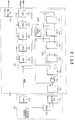
- Fig. 1 is a block diagram of the whole configuration of an image motion compensating address generator embodying the present invention;
- Fig. 2 is a detailed block diagram of the video mode selector and field/frame mode processor of Fig. 1;
- Fig. 3 is a detailed block diagram of the address selection controller of Fig. 1;
- Fig. 4 is a detailed block diagram of the Y-direction read address starting point operator of Fig. 1;
- Fig. 5 is a detailed block diagram of the processed-block unit Y-direction read address generator and video mode & motion coding type processing selector of Fig. 1;
- Fig. 6 is a detailed block diagram of the X-direction read address starting point operator of Fig. 1;
- Fig. 7 is a detailed block diagram of the processed-block unit X-direction read address generator of Fig. 1;
- Fig. 8 is a detailed block diagram of the processed-block unit X-direction write address generator of Fig. 1;
- Fig. 9 is a detailed block diagram of the Y-direction write address generator of Fig. 1;
- Fig. 10 is a detailed block diagram of the four-phase address generator of Fig. 1;
- Fig. 11 is a detailed block diagram of the X-direction read & write selector of Fig. 1; and
- Fig. 12 is a detailed block diagram of the Y-direction read & write selector of Fig. 1.
- Hereinafter, a preferred embodiment of the present invention will be described with reference to the attached drawings.
- Referring to Fig. 1, an image motion compensating address generator embodying the invention comprises a
mode selector 1, anaddress selection controller 2, a Y-directionread address generator 3, an X-directionread address generator 4, an X-directionwrite address generator 5, a Y-directionwrite address generator 6, and a read & writecontroller 7. -
Mode selector 1 comprises avideo mode selector 11 for determining whether an address is generated in a field mode or frame mode according to a video mode signal pstr1 orpstr 0 indicative of whether an input video signal is frame or field unit, and a field/frame mode processor 12 for establishing the position of slice in the field mode and frame node according to a signal output fromvideo mode selector 11 and a slice position signal SVP indicative of the position of slice. The mode selector selects the field mode or frame mode according to input video mode signal pstr1 or pstr0 and slice position signal SVP, to thereby control the video signal to be processed. -
Address selection controller 2 controls the generation of addresses according to video mode signal pstr1 or pstro and a motion coding type signal indicative of the video processing mode of a block to be processed, that is, a macroblock, which is the unit of processing the video signal. - Y-direction
read address generator 3 comprises a Y-direction read addressstarting point operator 31 for operating the Y-direction starting point of a processed block to read, according to the signal output from field/frame mode processor 12 and a Y-direction motion vector signal mvy indicative of the degree of Y-direction motion, a processed-block unit Y-direction readaddress generator 32 for generating Y-direction read addresses of several modes so that the signal output from Y-direction read addressstarting point operator 31 coincides with the processed block, and a video mode & motion codingtype processing selector 33 for including into one bit of the lower level a vertical field selection signal mvfs for selecting a upper or lower field according to motion information, out of the signals output from processed-block unit Y-direction readaddress generator 32 according toaddress selection controller 2, to thereby outputting a Y-direction read address fit for the respective modes. The Y-direction read address generator produces the Y-direction read address in units of processed block by using the signal output from field/frame mode processor 12 ofmode selector 1 according toaddress selection controller 2, Y-direction motion vector signal mvy, and vertical field selection signal mvfs. - X-direction
read address generator 4 comprises an X-direction read address starting point operator 41 for operating the X-direction starting point of the processed block to read by using a processed-block position signal MBA indicative of the X-direction position of the processed block and an X-direction motion vector signal mvx indicative of the degree of X-direction motion, and a processed-block unit X-direction readaddress generator 42 for dividing the processed block into four phases and generating the X-direction read address by using the signal output from X-direction read address starting point operator 41 acccrding to addressselection controller 2. The X-direction read address generator divides the processed block into four phases in the X direction and generates the X-direction read address by using processed-block position signal MBA and X-direction motion vector signal mvx according toaddress selection controller 2. - X-direction
write address generator 5 comprises an X-direction writeaddress delay controller 51 for delaying processed-block position signal MBA for a predetermined time so as to rewrite read-out video data, and an X-directionwrite address generator 53 for dividing the processed block into four phases and generating the X-direction write address by using the signal output from X-direction writeaddress delay controller 51. The X-direction write address generator delays processed-block positicn signal MBA and generates the X-direction write address of four phases, to thereby write the read-out video data. - Y-direction
write address generator 6 comprises a Y-directionwrite address generator 61 for generating a Y-direction write address in units of processed block by using the signal output from field/frame mode processor 12 ofmode selector 1 according to X-direction writeaddress delay controller 51 of X-directionwrite address generator 5, and a video mode & motion codingtype processing selector 62 for selectively outputting the Y-direction write address fit for the respective modes among the signals output from Y-directionwrite address generator 61 according toaddress selection controller 2. In order to write the read-out video data, the Y-direction write address generator produces the Y-direction write address by using the signal output from field/frame mode processor 12 ofmode selector 1 according toaddress selection controller 2 and X-direction writeaddress delay controller 51 of X-directionwrite address generator 5. - Read & write
controller 7 comprises a Y-direction read & writeselector 73 for selectively outputting one of the Y-direction read address and Y-direction write address output from video mode & motion codingtype processing selector 33 of Y-direction readaddress generator 3 and video mode & motion codingtype processing selector 62 of Y-directionwrite address generator 6 according to a read/write selection toggle signal for controlling the read & write operation, a four-phase address generator 71 for compensating for the X-direction read address output from processed-block unit X-directionread address generator 42 of X-direction readaddress generator 4 according to the read/write selection toggle signal, and an X-direction read & writeselector 72 for selecting one of the X-direction read address and X-direction write address output from the four-phase address generator 71 and X-directionwrite address generator 53 of X-direction writeaddress generator 5 and dividely outputting the selected address in four phases according to the read/write selection toggle signal. The read & write controller selectively outputs the X-direction and Y-direction read and write addresses according to the read/write selection toggle signal among X-direction and Y-direction read and write addresses output from Y-direction readaddress generator 3, X-direction readaddress generator 4, X-directionwrite address generator 5 and Y-directionwrite address generator 6. - The operation of the image motion compensating address generator will be explained below.
- A two-bit motion coding type signal indicative of the video processing mode of 16-by-16 pixels of a macroblock, that is, the processed block which is the unit of processing the video signal, is input to address
selection controller 2 along with video mode signal pstr1 or pstr0 indicative of whether the input video signal is frame or field unit. In order to determine the compensating method of the processed block unit, the input signal outputs a processing selection control signal for controlling the signal to be processed according to modes, and outputs a preset signal for presetting processed-block unit X-direction readaddress generator 42 when it counts. - Specifically, if video mode signal pstr1 or pstr0 is "11" in the frame mode and the motion coding type signal is "01," the mode becomes a field base mode in which the video signal of the processed block is processed in units of field. If video mode signal pstr1 or pstr0 is "11" in the frame mode and the motion coding type signal is "10," the mode becomes a frame base mode in which the video signal of the processed block is processed in units of frame. If video mode signal pstr1 or pstr0 is "01" or "10" in the field mode and the notion coding type signal is "01," the mode becomes the field base mode in which the video signal of the processed block is processed in units of field. If video mode signal pstr1 or pstr0 is "01" or "10" in the frame mode and the motion coding type signal is "10," the mode becomes a 16-by-8 base mode in which the processed block is processed in 16-by-8 units, which is half the macroblock.
- Video mode signal pstr1 or pstr0 indicative of whether the input video signal is frame or field unit determines whether
video mode selector 11 ofmode selector 1 generates its address in the field or frame mode. - Slice position signal SVP indicative of the Y-direction position is output from field/
frame mode processor 12 as a signal for setting the position of slice so that it is fit for the field mode and frame mode, according to the signal output fromvideo mode selector 11. - If video mode signal pstr1 or pstr0 is "11," the input video signal indicates the frame unit. In this case, a signal for controlling the address to be generated in the frame mode in which the video signal is processed in units of frame is output from
video mode selector 11 so that slice position signal SVP passes through field/frame mode processor 12 without change. - If video mode signal pstr1 or pstr0 is "01," the input video signal indicates the upper ficld in units of field. In this case, a signal for controlling the address to be generated in the field mode in which the video signal is processed in units of field is output from
video mode selector 11 so that slice position signal SVP is doubled and thereby a signal twice slice position signal SVP is output from field/frame mode processor 12. - If video mode signal pstr1 or pstr0 is "10," the input video signal indicates the lower field in units of field. In this case, a signal for controlling the address to be generated in the field mode in which the video signal is processed in units of field is output from
video mode selector 11 so that slice position signal SVP is doubled and thereby a signal twice slice position signal SVP is output from field/frame mode processor 12. - The operation of generating the X-direction and Y-direction read addresses according to the signals output from
mode selector 1 andaddress selection controller 2 will be explained below. - Slice position signal SVP or the signal twice slice position signal SVP output from field/
frame mode processor 12 is input to Y-direction read addressstarting point operator 31 along with Y-direction motion vector signal mvy so that the Y-direction starting point of the processed block to read is operated. - The signal output from field/
frame mode processor 12 is multiplied by 16, the Y-direction size of the processed block, in Y-direction read addressstarting point operator 31, in case that for instance, the processed block is a macroblock of 16-by-16 pixels. The multiplied signal is added to Y-direction motion vector signal mvy so that the Y-direction starting point of the processed block to read is output. - The signal corresponding to the Y-direction starting point of the processed block to read, which is the signal output from Y-direction
read address operator 31, is input to processed-block unit Y-direction readaddress generator 32. When main clocks mclk are input as many as the pixels divided into four phases in the X direction, the signal corresponding to the Y-direction starting point of the processed block to read increases by 1 and 2, generating the Y-direction read address of the frame and field modes fit for the processed block. - For instance, in case that the processed block is the macroblock of 16-by-16 pixels, whenever four main clocks mclk are applied corresponding to the number of pixels divided into four phases in the X direction, the signal corresponding to the Y-direction starting point of the processed block to read increases by 1 and 2, generating the Y-direction read address of the frame and field modes.
- The Y-direction read address of the frame and field modes output from processed-block unit Y-direction read
address generator 32 is selected by one in video mode & motion codingtype processing selector 33 by the processing selection control signal output fromaddress selection controller 2. - Here, when the Y-direction read address of the field mode is selected by
address selection controller 2, vertical field selection signal mvfs is contained in one bit of the lower level, outputting the Y-direction read address according to the upper or lower field. - In case of the upper field, vertical field selection signal mvfs becomes "0." In case of the lower field, vertical field selection signal mvfs becomes "1," controlling video mode & motion coding
type processing selector 33. - When the processed block is the macroblock of 16-by-16 pixels, the Y-direction read address is given as shown in the following table <TABLE 1>, according to the respective modes.


- As indicated in <TABLE 1>, there are two kinds of form in which the Y-direction read address is generated.
- First, as in column (A) of <TABLE 1>, the Y-direction read addresses of the processed block all are sequentially output in the frame mode. Second, as in columns (B), (C) and (D) of <TABLE 1>, the Y-direction read addresses of the processed block are doubled and read out every other line by the multiple of 2 and a value added to the multiple of 2 by "1."
- If video mode signal pstr1 or pstr0 corresponding to the first case is "11" and the motion coding type signal is "10" in the frame base mode, the Y-direction read addresses are output in "0, 1, 2, 3, ...16, 17," as shown in column (A) of <TABLE 1>, regardless of vertical field selection signal mvfs. Here, addresses "16 and 17" corresponding to the succeeding macroblock are generated at the end of the Y-direction addresses so that they are to be used when necessary to be read out additionally in case that the half pel compensation is employed.
- If video mode signal pstr1 or pstr0 corresponding to the first case is "11," the motion coding type signal is "01" in the field base mode, and vertical field selection signal mvfs is "0," as shown in column (B) of <TABLE 1>, the Y-direction read addresses are output in "0, 2, 4, 6, ...16," in the upper field. If vertical field selection signal mvfs is "1," the Y-direction read addresses are output in "1, 3, 5, 7, 9,..,17," in the lower field. Addresses "0, 2, 4, 6, ... 16" and "1, 3. 5, 7, 9, ... 17" are output again because the addresses are reset by the processing selection control signal output from
address selection controller 2. Here, addresses "16 and 17" corresponding to the succeeding macroblock are generated at the end of the Y-direction read addresses so that they are to be used when necessary to be read out additionally in case that the half pel compensation is employed. - If video mode signal pstr1 or pstr0 corresponding to the second case is "01" or "10," the motion coding type signal is "01" in the field base mode, and vertical field selection signal mvfs is "0," as shown in column (C) of <TABLE 1>, the Y-direction read addresses are output in "0, 2, 4, 6, ...16," in the upper field. If vertical field selection signal mvfs is "1," the Y-direction read addresses are output in "1, 3, 5, 7, 9,...17," in the lower field. Sequentially, addresses "18, 20, ..., 30, 32, 34" and "19, 21, ..., 31, 33, 35" are output because the addresses are not reset by the processing selection control signal output from
address selection controller 2. Here, addresses "32 and 34" and "33 and 35" corresponding to the succeeding macroblock are generated at the end of the Y-direction read addresses so that they are to be used when necessary to be read out additionally in case that the half pel compensation is employed. - If video mode signal pstr1 or pstr0 corresponding to the second case is "01" or "10," the motion coding type signal is "10" in the 16-by-8 base mode, and vertical field selection signal mvfs is "0," as shown in column (D) of <TABLE 1>, the Y-direction read addresses are output in "0, 2, 4, 6, ...16," in the upper field. If vertical field selection signal mvfs is "1," the Y-direction read addresses are output in "1, 3, 5, 7, 9,...17," in the lower field. Sequentially, addresses "0, 2, 4, 6, ... 16" and "1, , 5, 7, 9, ... 15, 17" are output again because the addresses are reset by the processing selection control signal output from
address selection controller 2. Here, addresses "16 and 17" corresponding to the succeeding macroblock are generated at the end of the Y-direction read addresses so that they are to be used when necessary to be read out additionally in case that the half pel compensation is employed. - As stated above, since the address generating forms are divided into two according to one bit of the high level of the motion coding type signal, only one bit of the high level of the two bit notion coding type signal can be used in control.
- Processed-block position signal MBA indicative of the X-direction position of the processed block is input to X-direction read address starting point operator 41 along with X-direction motion vector signal mvx so that the X-direction starting point of the processed block to read is operated.
- Processed-block position signal MBA is multiplied by 16, the X-direction size of the processed block, in X-direction read address starting point operator 41, in case that for instance, the processed block is a macroblock of 16-by-16 pixels. The multiplied signal is added to X-direction motion vector signal mvx so that the X-direction starting point of the processed block to read is output.
- The signal corresponding to the X-direction starting point of the processed block to read, which is the signal output from X-direction read address operator 41, is input to processed-block unit X-direction
road address generator 42, increasing by one whenever main clock mclk is produced. When main clocks mclk are input as many as the pixels divided into four phases in the X direction, the signal corresponding to the X-direction starting point of the processed block to read is preset according toaddress selection controller 2 and then increases by one whenever main clock mclk is produced. This procedure is repeated until one processed-block all is read, that is, until the Y-direction read addresses of the block all are produced, generating the X-direction read address. The process of generating the X-direction and Y-direction read addresses will be described below. - First, the signal output from field/
frame mode processor 12 and Y-direction motion vector signal mvy are operated in Y-direction read addressstarting point operator 31, outputting the Y-direction read address corresponding to the Y-direction starting point of the processed block to read. - Processed-block position signal MBA and X-direction motion vector signal mvx are operated in X-direction read address starting point operator 41, outputting the X-direction read address corresponding to the X-direction starting point of the processed block to read. By doing so, the starting points of the processed block to read can be obtained.
- The X-direction read address corresponding to the X-direction starting point of the processed block to read is produced, increasing by one whenever main clock mclk is input in processed-block unit X-direction read
address generator 42. For instance, in case that the processed block is the macroblock of 16-by-16 pixels, whenever four main clocks mclk are produced, corresponding to the number of pixels in which the processed block is divided into four phases according toaddress selection controller 2, the signal corresponding to the X-direction starting point is preset and increases from the beginning. - Whenever the X-direction read address increases by one and is preset, that is, when four main clocks mclk are produced, the Y-direction read address corresponding to the Y-direction starting point of the processed block to read increases by one or two, corresponding to the frame mode and field mode, and then is input to video mode & motion coding
type processing selector 33. - The Y-direction read addresses output from processed-block unit Y-direction read
address generator 32 are selected into one of the two frame mode and field mode according to the processing selection control signal output fromaddress selection controller 2. - The operation of generating the X-direction and Y-direction write addresses according to the signal output from
mode selector 1 andaddress selection controller 2 will be described below in detail. - Processed-block position signal MBA delays video data read out by X-direction write
address delay controller 51 for a predetermined period for the purpose of rewriting. This can be explained in this way. The video signal is stored in a memory in units of frame. When a succeeding frame is input, video data of the preceding frame is read out and output, and video data of the current frame is read out, compensated for motion, and then stored in the memory which stores the preceding frame. The succeeding frame is stored in the memory which stores the current frame. Therefore, a predetermined time of delay is required until read video data are compensated for motion and rewritten. - Here, until video data of one frame is read, compensated for motion, and rewritten in the memory, 311 main clocks mclk are generated. While the 311 main clocks mclk are generated, processed-block position signal MBA input to X-direction write
address delay controller 51 must be delayed. - Processed-block positicn signal MBA delayed and output from X-direction write
address delay controller 51 is input to X-direction writeaddress generator 53, dividing the processed block into four phases in the X direction and generating the X-direction write address according to main clock mclk. - For instance, in case that the processed block is the 16-by-16 macroblock, the block is divided into four phases in the X direction. Whenever the main clock is input, the X-direction write address corresponding to processed-block position signal MBA is generated by increasing by one. When four main clocks mclk are input, the X-direction write address is preset, producing the X-direction write address corresponding to processed-block position signal MBA repeatedly from the beginning. Whenever four main clocks mclk are input, the X-direction write address is preset so that only the lower two bits are counted.
- Slice position signal SVP or a signal double slice position signal SVP output from field/
frame mode processor 12 increases by one or two in Y-directionwrite address generator 61 according to X-direction writeaddress delay controller 51, when main clock mclk is input as many as pixels in which the processed block is divided into four phases in the X direction. By doing so, the Y-direction write address of the frame mode and field mode is generated to be fit for the processed block. - For instance, in case that the processed block is the 16-by-16 macroblock, whenever four main clocks mclk are applied corresponding to pixels divided into four phases in the X direction, the signal increases by one or two, generating the Y-direction write address of the frame mode and field mode. The Y-direction write address of the frame mode and field mode output from Y-direction
write address generator 61 is selected into one mode in video mode & motion codingtype processing selector 62, by the processing selection signal output fromaddress selection controller 2. - The operation of generating the X-direction and Y-direction write addresses will be explained below.
- First, in order to delay the generation of the X-direction write address as long as the time during which data read by X-direction write
address delay controller 51 is rewritten in the frame-unit memory after several processes, processed-block position signal MBA is delayed and input to X-direction writeaddress generator 53. - Delayed processed-block position signal MBA increases by one whenever main clock mclk is input to X-direction write
address generator 53, producing the X-direction write address. In case that the processed block is the macroblock of 16-by-16, when four main clocks mclk, which is the number of pixels in which the processed block is divided into four phases, the signal is preset so that the X-direction write address corresponding to processed-block position signal MBA increases repeatedly from the beginning. - Whenever the X-direction read address incresses by one and is preset, that is, whenever four main clocks mclk are produced, the Y-direction write address corresponding to the signal output from field/
frame mode processor 12 increases by one and two, corresponding to the frame mode and field mode. The address is input to video mode & motion codingtype processing selector 62. - The Y-direction write addresses output from Y-direction
write address generator 61 are selected into one of the frame mode and field mode according to the processing selection control signal output fromaddress selection controller 2. - The X-direction read address output from processed-block unit X-direction read
address generator 42 is input to four-phase address generator 71 of read & writecontroller 7, and divided into four phases by the read/write selection toggle signal and the lower two bits bmvx 0, 1 andfmvx - The X-direction write address output from X-direction
write address generator 53 and the four-phase X-direction read address output from four-phase address generator 71 are input to X-direction read & writeselector 72 of read & writecontroller 7. Reading and writing of these addresses are determined and selected according to the read/write selection toggle signal. - The Y-direction read address and Y-direction write address output from video mode & motion coding
type processing selectors selector 73 of read & writecontroller 7. Reading and writing of these addresses are determined and selected according to the read/write selection toggle signal. - The detailed configuration and operation of the respective components of the present embodiment will be described with reference to Figs. 2-12.
- Referring to Fig. 2,
video mode selector 11 comprises aNAND gate 111 for NAND-operating video mode signal pstr1 or pstr0 and outputting it to field/frame mode processor 12. - If video mode signal pstr1 or pstr0 is "11," the output of
NAND gate 111 becomes "0," controlling the video signal to be processed in the frame mode. - If video mode signal pstr1 or pstr0 is "01" or "10," the output of
NAND gate 111 becomes "1," controlling the video signal to be processed in the field mode. - Field/
frame mode processor 12 comprises amultiplexer 121 for selecting one of slice position signal SVP and a signal double slice position signal SVP according to the signal output fromNAND gate 111 ofvideo mode selector 11, as shown in Fig. 2. - If the signal output from
NAND gate 111 indicates the frame mode as "0," slice position signal SVP is output frommultiplexer 121 without change. If the signal output fromNAND gate 111 indicates the field mode as "1," a signal in which slice position signal SVP is shifted upward by one bit, that is, the signal double slice position signal SVP, is output frommultiplexer 121. -
Multiplexer 121 receives slice position signal SVP and the signal in which slice position signal SVP is shifted by one bit, and selects one according toNAND gate 111. - Referring to Fig. 3, address selection controller 2 comprises a control signal generator 21 for receiving video mode signal pstr1 or pstr0 and the motion coding type signal, and outputting the processing selection control signal for controlling the selection of modes and another control signal to processed-block unit X-direction read address generator 42 and video mode & motion coding type processing selectors 33 and 62, a first delay 22 for delaying a frame processed-block clock signal mbclk for processing the processed-block in frames in order for synchronization with the processing selection control signal and control signal output from control signal generator 21, a second delay 23 for delaying a field processed-block clock signal mbsync for processing the processed-block in fields in order for synchronization with the processing selection control signal and control signal output from control signal generator 21, a multiplexer 24 for selecting one of the signals output from first and second delays 22 and 23 according to the delay signal of control signal generator 21, a counter 26 for counting to preset the X-direction read address according to main clock mclk, a third delay 25 for delaying the signal output from multiplexer 24 in order for synchronization with the signal output from counter 26, and an AND gate 27 for AND-operating the signal output from third delay 25 and the signal output from counter 26 and outputting a preset signal for presetting the X-direction read address for a predetermined period. Here, counter 26 can lengthen the period of presetting the X-direction read address by using the clear port in case that the half pel is used.
-
Control signal generator 21 comprises an ANDgate 211 for AND-operating video mode signal pstr1 or pstr0, an exclusive-OR gate 213 for EXCLUSIVE-OR-operating the signal output from ANDgate 211 and the motion coding type signal to thereby controlmultiplexer 24, and aNAND gate 212 for NAND-operating video mode signal pstr1 or pstr0 and the motion coding type signal and outputting the processing selection control signal. - Video mode signal pstr1 or pstr0 is AND-operated in AND
gate 211, being output as "1" in the frame mode and as "0" in the field mode. - The signal output from AND
gate 211 is EXCLUSIVE-OR-operated with the motion coding type signal indicative of the coding type of the processed block, controllingmultiplexer 24. - When the signal indicating that the motion coding type signal of the frame mode is processed in fields is output from AND
gate 211, the signal is EXCLUSIVE-OR-operated in EXCLUSIVE-OR gate 213 so thatmultiplexer 24 is controlled to select field processed-block clock signal mbsync delayed insecond delay 23. - When the signal indicating that the motion coding type signal of the frame mode is processed in frames is output from AND
gate 211, the signal is EXCLUSIVE-OR-operated in EXCLUSIVE-OR gate 213 so thatmultiplexer 24 is controlled to select frame processed-block clock signal mbclk delayed infirst delay 22. - When the signal indicating that the motion coding type signal of the field mode is processed in frames is output from AND
gate 211, the signal is EXCLUSIVE-OR-operated in EXCLUSIVE-OR gate 213 so thatmultiplexer 24 is controlled to select field processed-block clock signal mbsync delayed insecond delay 23. The signal output frommultiplexer 24 is delayed until the signal ofcounter 26 is output fromthird delay 25. -
Counter 26 produces a signal for presetting the X-direction read address whenever four main clocks mclk are input which is the number of the pixels divided into four phases in the X direction. In case of the half pel compensation, whenever every five main clock mclk is input, the counter is cleared for one clock and performs counting again, reading nearby pixel data which is then used in compensation. - Referring to Fig. 4, Y-direction read address
starting point operator 31 comprises first, second and third serially coupledadders frame mode processor 12 and adding Y-direction motion vector signal mvy, and alatch 314 for stabilizing the signal output from first, second andthird adders - The signal output from field/
frame mode processor 12 and indicative of the Y-direction position of the processed block is multiplied by number 16 which is the Y-direction size of the processed block by first, second andthird adders - The signals output from first, second and
third adders latch 314, and output to processed-block unit Y-direction readaddress generator 32. - Referring to Fig. 5, processed-block unit Y-direction read
address generator 32 comprises afirst counter 321 for receiving the signal output fromlatch 314 of Y-direction read addressstarting point operator 31 and counting to generate the Y-direction read address fit for the frame mode, and asecond counter 322 for shifting the signal output fromlatch 314 and counting to generate the Y-direction read address fit for the field mode. - First and
second counters address generator 32 generate Y-direction read addresses fit for the frame mode and field mode, respectively. - The signal output from
latch 314 of Y-direction read addressstarting point operator 31 increases by one infirst counter 321 whenever four main clocks mclk are generated which is the number of pixels in which the X-direction pixels of the processed block are divided into four phases, producing the Y-direction read address of the frame mode. - The signal output from
latch 314 increases by two insecond counter 322 whenever four main clocks mclk are generated which is the number of pixels in which the X-direction pixels of the processed block are divided into four phases, producing the Y-direction read address of the field mode. - Referring to Fig. 5, video mode & motion coding
type processing selector 33 comprises amultiplexer 331 for selecting the Y-direction read address of one mode of the frame-mode Y-direction read address and field-mode Y-direction read address output from processed-block unit Y-direction readaddress generator 32 according toaddress selection controller 2, and if the field-mode Y-direction read address is selected, including vertical field selection signal mvfs into one bit of the lower level, and alatch 332 for stabilizing the signal output frommultiplexer 331. - The frame-mode Y-direction read address output from
first counter 321 and the field-mode Y-direction read address output fromsecond counter 322 are selected inmultiplexer 331 by the processing selection control signal output fromcontrol signal generator 21. - Here, when the field-mode Y-direction read address output from
second counter 322 is selected, vertical field selection signal mvfs indicative of the upper and lower fields are contained in one bit of the lower level so that the Y-direction read addresses corresponding to the upper and lower fields are output to latch 332. - The Y-direction read address output from
multiplexer 331 is synchronized and stabilized inlatch 332 and output to Y-direction read & writeselector 73 of read & writecontroller 7. - Referring to Fig. 6, X-direction read address starting point operator 41 comprises first and
second latches adders first latch 411 and adding the signal output fromsecond latch 412, and athird latch 416 for stabilizing the signal output from first, second andthird adders - The input time points of processed-block position signal MBA and X-direction motion vector signal mvx may be different. Therefore, their time points are made to coincide in first and
second latches third adders - The signals output from first, second and
third adders third latch 416, and output to processed-block unit X-direction readaddress generator 42. - Referring to Fig. 7, processed-block unit X-direction read
address generator 42 comprises acounter 421 for receiving the signal output fromthird latch 416 of X-direction read address starting point operator 41, being preset according to a preset signal output fromaddress selection controller 2, dividing the processed block in four phases in the X direction and counting to generate the X-direction read address, and alatch 422 for stabilizing the signal output fromcounter 421. - Here, in case of the half pel, counter 421 may be preset for a period in which the value in which the processed block is divided into four phases in the X direction, that is,
number 4, is added by one bycounter 26 ofaddress selection controller 2. - The signal corresponding to the starting point of the X-direction read address of the processed block to read, that is, the signal output from
third latch 416 of X-direction read address starting point operator 41, is input to counter 421 and increases by one whenever main clock mclk is produced. When the main clock is input as many as the pixels in which the processed block is divided into four phases in the X direction or the number in which one is added to the number of the pixels, the signal is preset according to the preset signal output fromaddress selection controller 2. The signal increases again by one whenever main clock mclk is produced. This process is repeated until one processed block all is read. - The signal output from
counter 421 is synchronized and stabilized inlatch 422, and input to four-phase address generator 71 of read & writecontroller 7. - Referring to Fig. 8, X-direction write address delay controller 51 comprises a first D flipflop 511 for receiving frame processed-block clock signal mbclk for processing the processed block in frames and outputting a clock signal, a latch portion 525 having a plurality of serially coupled latches 512, 513, 514, 515, and 516 for receiving the signal output from first D flipflop 511 as a clock input and delaying processed block clock signal mbsync for processing the processed block in fields and processed-block position signal MBA for a predetermined time, a first counter 521 for receiving main clock signal mclk and performing counting, a D flipflop portion 526 having a plurality of serially coupled flipflops 517, 518, 519, and 520 for receiving the signal output from first counter 521 as a clock input and delaying field processed-block clock signal delayed and output from latch portion 525 for a predetermined time, a second D flipflop 522 for receiving main clock signal mclk as a clock input and receiving the field processed-block clock signal mbsync delayed and output from D flipflop portion 526 as data input, an EXCLUSIVE-NOR gate 523 for EXCLUSIVE-NOR-operating the data input signal and output signal of second D flipflop 522, and a third D flipflop 524 for receiving the signal output from EXCLUSIVE-NOR gate 523 as data input and receiving main clock signal mclk as the clock input.
- Frame processed-block clock signal mbclk is input to the clear port of
latches latch portion 525 viafirst D flipflop 511, delaying processed-block position signal MBA and field processed-block clock signal mbsync. - Here, processed-block position signal MBA and field processed-block clock signal mbsync are delayed while frame processed-block clock signal mbclk is input by
latches - Since
latches latches - Processed-block position signal MBA delayed through
latch portion 525 is input to X-direction writeaddress generator 53. Field processed-block clock signal mbsync is input toD flipflop portion 526 and delayed for a time where the 64 main clocks are not input. - The output signal of
first counter 521 increases by one whenever 16 main clocks mclk are generated, is input to the clock input port of D flipflops 517, 518, 519 and 520 ofD flipflop portion 526, and delayed while 16 main clocks are input. - D flipflops 518, 519 and 520 delay the output signal of
first counter 521 while the 16 main clocks are input, the total delay time of D flipflops 518, 519 and 520 becomes the time to generate 16-by-3 main clocks. - Field processed-block clock signal mbsync delayed in
D flipflop portion 526 and output fromD flipflop 520 is input to second D flipflop 522 to be EXCLUSIVE-NOR-operated with field processed-block clock signal mbsync delayed and output until main clock mclk is input. Then, a preset signal is generated to preset the counter in units of processed block and make the output of the counter as "0." The preset signal is delayed via third D flipflop 524 by main clock mclk, and output to X-direction writeaddress generator 53. - Referring to Fig. 8, X-direction
write address generator 53 comprises asecond counter 531 for counting only two bits by taking the signal output from third D flipflop 524 of X-direction writeaddress delay controller 51 as the reset signal, alatch 533 for temporarily storing and stabilizing processed-block position signal MBA delayed and output fromlatch portion 525, and adelay 532 for delaying the signal output fromsecond counter 531 for the purpose of synchronization. - The signal output from third D flipflop 524 resets
second counter 531 whenever four main clocks mclk are produced.Second counter 531 counts only the two bits of the lower level of the output signal ofthird D flipflop 524. The output of the counter is synchronized throughdelay 532 and becomes the X-direction write address along with processed-block position signal MBA output fromlatch portion 525. The address is output to X-direction read & writeselector 72 of read & writecontroller 7. - Here,
second counter 531 counts only the two bits of the lower level of the output signal of third D flipflop 524 in case that the processed block is the 16-by-16 block. In this case, a signal divided into four pixels and indicative of four pixels may be output. Therefore, only the two bits of the lower level are varied sequentially and reset. - Referring to Fig. 9, Y-direction
write address generator 61 comprises acounter 611 preset according to the signal output from X-direction writeaddress delay controller 51 and for multiplying the Y-direction size of the processed-block unit to the signal output from field/frame mode processor 12 ofmode selector 1, and counting periodically according to main clock signal mclk. Counter 611 counts whenever the X-direction write addresses divided into four phases by main clock mclk are all generated and preset. -
Counter 611 uses only the higher bits of the output signal excluding the two bits of the lower level, not using the two bits of the lower level. - When the signal is output from third D flipflop 524 of X-direction write
address delay controller 51, counter starts operating so that the signal output from field/frame mode processor 12 increases by one or two, generating the Y-direction write address. - Here, in order to increase the signal output from field/
frame mode processor 12 ofmode selector 1 by two, counter 611 shifts one bit of the lower level which is then output to video mode & motion codingtype processing selector 62. - Referring to Fig. 9, video mode & motion coding
type processing selector 62 comprises amultiplexer 621 for selecting one of the output signal ofcounter 611 and the shifted output signal ofcounter 611 according toaddress selection controller 2, and alatch 622 for stabilizing the signal output frommultiplexer 621. - The frame-mode Y-direction write address in which one bit of the lower level is not shifted and the field-mode Y-direction read address in which one bit of the lower level is shifted are selected in
multiplexer 621 according to the processing selection control signal output fromcontrol signal generator 21. - The Y-direction write address output from
multiplexer 621 is synchronized and stabilized inlatch 622, and output to Y-direction read & writeselector 73 of read & writecontroller 7. - Referring to Fig. 10, four-
phase address generator 71 comprises acompensation controller 710 for controlling the compensation of the X-direction read address divided into four phases by using the read/write selection toggle signal and the two bit signals bmvx0,1 and fmvx0,1 of the lower level of the X-direction motion vector signal of the backward and forward frames, first, second andthird latches address generator 42 of X-direction readaddress generator 4 according tocompensation controller 710, and afourth latch 714 for latching the X-direction read address output from processed-block unit X-direction readaddress generator 42 of X-direction readaddress generator 4 according to the low-level signal 0. The four-phase address generator produces the X-direction read address divided into four phases. -
Compensation controller 710 comprises afirst multiplexer 715 for selecting one of the lowest bit signals bmvx0 and fmvx0 of the X-direction motion vector signal of the backward and forward frames according to the read/write selection toggle signal, asecond multiplexer 716 for selecting one of the second lowest bit signals bmvx1 and fmvx1 of the X-direction motion vector signal of the backward and forward frames according to the read/write selection toggle signal, an ORgate 717 for OR-operating the signals output from first andsecond multiplexers first latch 711, abuffer 718 for delaying the signal output fromsecond multiplexer 716 and outputting a signal CIN2 for controllingsecond latch 712, and an ANDgate 719 for OR-operating the signals output from first andsecond multiplexers third latch 713. - The read/write selection toggle signal for changing the memory for storing the video signal data allows first and
second multiplexers - Signals xpcon 0,1 selected and output from first and
second multiplexers OR gate 717 to controlfirst latch 711.Signal xpcon 1 output fromsecond multiplexer 716 is delayed and synchronized inbuffer 718 to controlsecond latch 712. Signals xpcon 0,1 output from first andsecond multiplexers gate 719 to controlthird latch 713. - In case that the X-direction read address is divided by 4 and its remainder is 3, first,
fourth latch 714 generates the X-direction read address, and then high-level signals are output from ORgate 717,buffer 718 and ANDgate 719 so that the X-direction read addresses are generated sequentially. - In case that the X-direction read address is divided by 4 and its remainder is 0, low-level signals are output from OR
gate 717,buffer 718 and ANDgate 719 so that the X-direction read addresses are generated simultaneously in first, second, third andfourth latches - In case that the X-direction read address is divided by 4 and its remainder is 1, first, second, third and
fourth latches buffer 718 and ANDgate 719 so that the X-directlon read addresses are generated sequentially. - In case that the X-direction read address is divided by 4 and its remainder is 2, first, third and
fourth latches gate 719 so that the X-direction read addresses are generated sequentially. - The four-phase X-direction read addresses output from first, second, third and
fourth latches selector 72 of read & writecontroller 7. - Referring to Fig. 11, X-direction read & write
selector 72 comprises first, second, third andfourth multiplexers phase address generator 71 and X-directionwrite address generator 53 according to read/write selection toggle signal, and first, second, third andfourth latches multiplexers - In case that the read/write selection toggle signal indicates a reading mode, first, second, third and
fourth multiplexers phase address generator 71. - In case that the read/write selection toggle signal indicates a writing mode, first, second, third and
fourth multiplexers write address generator 53. - The X-direction read address and X-direction write address selected by first, second, third and
fourth multiplexers fourth latches - Referring to Fig. 12, Y-direction read & write
selector 73 comprises amultiplexer 731 for selecting one of the Y-direction read address and Y-direction write address output from video mode & codingtype processing selectors address generator 3 and Y-directionwrite address generator 6 according to the read/write selection toggle signal, and alatch 732 for stabilizing the Y-direction read address and Y-direction write address output frommultiplexer 731. - In case that the read/write selection toggle signal indicates a reading mode,
multiplexer 731 selects the Y-direction read addresses output from video mode & motion codingtype processing selector 33 of Y-direction readaddress generator 3. In case that the read/write selection toggle signal indicates a writing mode,multiplexer 731 selects the Y-direction write addresses output from video mode & motion codingtype processing selector 62 of Y-directionwrite address generator 6. - The Y-direction read address and Y-direction write address selected by
multiplexer 731 are stabilized inlatch 732. - As described above, the present embodiment implements the high level of the main profile of the MPEG II algorithm with hardware, allowing the MPEG II algorithm to be employed in HDTVs or HDVCRs.
- Since the standard of a digital high-definition television (HDTV) which is highly marketable in US and the like follows the high level of the main profile of the MPEG II algorithm, the described embodiment allows this algorithm to be implemented in a stabler and more commercially useful designing method, fostering the development of HDTVs and HDVCRs.
Claims (28)
- An image motion compensating address generator comprising:
mode selector means for selecting a field mode or frame mode according to a video mode signal indicative of whether an input video signal is a frame unit or field unit and a slice position signal indicative of the position of slice, to thereby control the video signal to be processed;
address selection controller means for controlling the generation of addresses according to the video mode signal and a motion coding type signal indicative of the video processing mode of a block to be processed;
Y-direction read address generator means for producing a Y-direction read address in units of processed block by using the signal output from the mode selector means according to the address selection controller means, a Y-direction motion vector signal, and a vertical field selection signal;
X-direction read address generator means for dividing the processed block into four phases in the X direction and generating an X-direction read address by using a processed-block position signal indicative of the position of the processed block and an X-direction motion vector signal according to the address selection controller means;
X-direction write address generator means for delaying the processed-block position signal and a field processed-block clock signal, and generating the X-direction write address of four phases, to thereby write read-out video data;
Y-direction write address generator means for producing a Y-direction write address by using the signal output from of the mode selector means according to the address selection controller means and the X-direction write address generator means, to thereby write read-out video data; and
read & write controller means for selectively outputting the X-direction and Y-direction read and write addresses according to a read/write selection toggle signal and an X-direction motion vector signal among the X-direction and Y-direction read and write addresses output from the Y-direction read address generator means, X-direction read address generator means, X-direction write address generator means and Y-direction write address generator means. - An image motion compensating address generator as claimed in claim 1, wherein the mode selector means comprises:
a video mode selector for determining whether an address is generated in a field mode or frame mode according to the video mode signal; and
a field/frame mode processor for establishing the position of slice in the field mode and frame mode according to the signal output from the video mode selector means and the slice position signal. - An image motion compensating address generator as claimed in claim 2, wherein the video mode selector comprises a NAND gate for NAND-operating the video mode signal and outputting it to the field/frame mode processor.
- An image motion compensating address generator as claimed in claim 2, wherein the field/frame mode processor comprises a multiplexer for selecting one of the slice position signal and a signal double the slice position signal according to the signal output from a NAND gate of the video mode selector.
- An image motion compensating address generator as claimed in claim 1, wherein the address selection controller means comprises:
a control signal generator for receiving the video mode signal and the motion coding type signal, and outputting a processing selection control signal for controlling the selection of modes and another control signal to the Y-direction read address generator means, X-direction read address generator means and Y-direction write address generator means;
a first delay for delaying a frame processed-block clock signal for processing the processed-block in frames in order for synchronization with the processing selection control signal and control signal output from the control signal generator;
a second delay for delaying a field processed-block clock signal for processing the processed-block in fields in order for synchronization with the processing selection control signal and control signal output from the control signal generator;
a multiplexer for selecting one of the signals output from the first and second delays according to the delay signal of the control signal generator;
a counter for counting to preset the X-direction read address according to an input main clock;
a third delay for delaying the signal output from the multiplexer 24 in order for synchronization with the signal output from the counter; and
an AND gate for AND-operating the signal output from the third delay and the signal output from the counter and outputting a preset signal for presetting the X-direction read address. - An image motion compensating address generator as claimed in claim 5, wherein the control signal generator comprises:
an AND gate for AND-operating the video mode signal;
an exclusive-OR gate for EXCLUSIVE-OR-operating the signal output from the AND gate and the motion coding type signal to thereby control the multiplexer; and
a NAND gate for NAND-operating the video mode signal and the motion coding type signal and outputting a processing selection control signal. - An image motion compensating address generator as claimed in claim 5, wherein the counter varies the period of presetting the X-direction read address by using a clear port in case that a half pel is used.
- An image motion compensating address generator as claimed in claim 1, wherein the Y-direction read address generator means comprises:
a Y-direction read address starting point operator for operating the Y-direction starting point of a processed block to read, according to the signal output from the field/frame mode processor of the mode selector means and a Y-direction motion vector signal;
a processed-block unit Y-direction read address generator for generating Y-direction read addresses of several modes so that the signal output from the Y-direction read address starting point operator coincides with the processed block; and
a video mode & motion coding type processing selector for receiving a signal output from the processed-block unit Y-direction read address generator and a vertical field selection signal according to the address selection controller means, to thereby outputting a Y-direction read address fit for the respective modes. - An image motion compensating address generator as claimed in claim 8, wherein the Y-direction read address starting point operator comprises:
first, second and third serially coupled adders for multiplying the Y-direction size of the processed block to the signal output from the field/frame mode processor of the mode selector means and adding a Y-direction motion vector signal; and
a latch for stabilizing the signals output from the first, second and third adders. - An image motion compensating address generator as claimed in claim 8, wherein the processed-block unit Y-direction read address generator comprises:
a first counter for receiving the signal output from the latch of the Y-direction read address starting point operator and counting to generate the Y-direction read address fit for the frame mode; and
a second ccunter for shifting the signal output from the latch of the Y-direction read address starting point operator, and counting to generate the Y-direction read address fit for the field mode. - An image motion compensating address generator as claimed in claim 8, wherein the video mode & motion coding type processing selector comprises:
a multiplexer for selecting the Y-direction read address of one mode of frame-mode Y-direction read address and field-mode Y-direction read address output from the processed-block unit V-direction read address generator according to the address selection controller means, and if the field-mode Y-direction read address is selected, including a vertical field selection signal into one bit of the lower level; and
a latch for stabilizing the signal output from the multiplexer. - An image motion compensating address generator as claimed in claim 1, wherein the X-direction read address generator means comprises:
an X-direction read address starting point operator for operating the X-direction starting point of the processed block to read by using a processed-block position signal and an X-direction motion vector signal; and
a processed-block unit X-direction read address generator for receiving the signal output from the X-direction read address starting point operator according to the address selection controller means, dividing the processed block into four phases and generating the X-direction read address. - An image motion compensating address generator as claimed in claim 12, wherein the X-direction read address starting point operator comprises:
a first latch for latching the processed-block position signal for the purpose of synchronization;
a second latch for latching the X-direction motion vector signal for the purpose of synchronization;
first, second and third serially coupled adders for multiplying the X-direction size of the processed block unit to the signal output from the first latch and adding the signal output from the second latch; and
a third latch for stabilizing the signal output from the first, second and third adders. - An image motion compensating address generator as claimed in claim 12, wherein the processed-block unit X-direction read address generator comprises:
a counter for receiving the signal output from the third latch of the X-direction read address starting point operator, being preset according to a preset signal output from the address selection controller means, dividing the processed block in four phases in the X direction and counting to generate the X-direction read address; and
a latch for stabilizing the signal output from the counter. - An image motion compensating address generator as claimed in claim 14, wherein the counter is preset for a period in which a value in which the processed block is divided into four phases in the X direction, is added by one in case of half pel.
- An image motion compensating address generator as claimed in claim 1, wherein the X-direction write address generator means comprises:
an X-direction write address delay controller for delaying the processed-block position signal and field processed-block clock signal for a predetermined time so as to rewrite read-out video data; and
an X-direction write address generator for dividing the processed block into four phases and generating the X-direction write address by using the signal output from the X-direction write address delay controller. - An image motion compensating address generator as claimed in claim 16, wherein the X-direction write address delay controller comprises:
a first D flipflop for receiving a frame processed-block clock signal for processing the processed block in frames and outputting a clock signal;
a latch portion having a plurality of serially coupled latches for receiving the signal output from the first D flipflop as a clock input and delaying the processed block clock signal for processing the processed block in fields and the processed-block position signal for a predetermined time;
a first counter for receiving a main clock signal and performing counting;
a D flipflop portion having a plurality of serially coupled flipflops for receiving the signal output from the first counter as a clock input and delaying the field processed-block clock signal delayed and output from the latch portion for a predetermined time;
a second D flipflop for receiving the main clock signal as a clock input and receiving the field processed-block clock signal delayed and output from the D flipflop portion as data input;
an EXCLUSIVE-NOR gate for EXCLUSIVE-NOR-operating the data input signal and output signal of the second D flipflop; and
a third D flipflop for receiving the signal output from the EXCLUSIVE-NOR gate as data input and receiving the main clock signal as the clock input. - An image motion compensating address generator as claimed in claim 16, wherein the X-direction write address generator comprises:
a second counter for counting only two bits by taking the signal output from the third D flipflop of the X-direction write address delay controller as the reset signal;
a latch for temporarily storing and stabilizing the processed-block position signal delayed and output from the latch portion: and
a delay for delaying the signal output from the second counter for the purpose of synchronization. - An image motion compensating address generator as claimed in claim 1, wherein the Y-direction write address generator means comprises:
a Y-direction write address generator for generating a Y-direction write address in units of processed block by using the signal output from a field/frame mode processor of the mode selector means according to an X-direction write address delay controller of the X-direction write address generator means: and
a video mode & motion coding type processing selector for selectively outputting the Y-direction write address fit for the respective modes among the signals output from the Y-direction write address generator according to the address selection controller means. - An image motion compensating address generator as claimed in claim 19, wherein the Y-direction write address generator comprises:
a counter preset according to the signal output from the X-direction write address delay controller and for multiplying the Y-direction size of the processed-block unit to the signal output from the field/frame mode processor of the mode selector means, and counting periodically according to the main clock signal. - An image motion compensating address generator as claimed in claim 19, wherein the video mode & motion coding type processing selector comprises:
a multiplexer for selecting one of the output signal of the counter and the shifted output signal of the counter according to the address selection controller means; and
a latch for stabilizing the signal output from the multiplexer. - An image motion compensating address generator as claimed in claim 20, wherein the counter counts whenever the X-direction write addresses divided into four phases by the main clock are all generated and preset.
- An image motion compensating address generator as claimed in claim 22, wherein the counter uses only the higher bits of an output signal excluding the two bits of the lower level, not using the two bits of the lower level.
- An image motion compensating address generator as claimed in claim 1, wherein the read & write controller means comprises:
a Y-direction read & write selector for selectively outputting one of the Y-direction read address and Y-direction write address output from the Y-direction read address generator means and Y-direction write address generator means according to the read/write selection toggle signal;
a four-phase address generator for compensating for the X-direction read address output from the X-direction read address generator means according to the read/write selection toggle signal; and
an X-direction read & write selector for selecting one of the X-direction read address and X-direction write address output from the four-phase address generator and X-direction write address generator means and dividely outputting the selected address in four phases according to the read/write selection toggle signal. - An image motion compensating address generator as claimed in claim 24, wherein the four-phase address generator 71 comprises:
a compensation controller for controlling the compensation of the X-direction read address divided into four phases by using the read/write selection toggle signal and two bit signals of the lower level of the X-direction motion vector signal of the backward and forward frames;
first, second and third latches for latching the X-direction read address output from the processed-block unit X-direction read address generator of the X-direction read address generator means according tc the compensation controller; and
a fourth latch for latching the X-direction read address output from the processed-block unit X-direction read address generator of the X-direction read address generator means according to al ow-level signal. - An image motion compensating address generator as claimed in claim 25, wherein the compensation controller comprises:
a first multiplexer for selecting one of the lowest bit signals of the X-direction motion vector signal of the backward and forward frames according to the read/write selection toggle signal;
a second multiplexer for selecting one of the second lowest bit signals of the X-direction motion vector signal of the backward and forward frames according to the read/write selection toggle signal;
an OR gate for OR-operating the signals output from the first and second multiplexers and outputting a signal for controlling the first latch;
a buffer for delaying the signal output from the second multiplexer and outputting a signal for controlling the second latch; and
an AND gate for OR-operating the signals output from the first and second multiplexers and outputting a signal for controlling the third latch. - An image motion compensating address generator as claimed in claim 24, wherein the X-direction read & write selector comprises:
first, second, third and fourth multiplexers for selecting one of the X-direction read address and X-direction write address output from the four-phase address generator and X-direction write address generator means according to the read/write selection toggle signal; and
first, second, third and fourth latches for stabilizing the X-direction read address and X-direction write address output from the first, second, third and fourth multiplexers. - An image motion compensating address generator as claimed in claim 24, wherein the Y-direction read & write selector comprises:
a multiplexer for selecting one of the Y-direction read address and Y-direction write address output from the Y-direction read address generator means and Y-direction write address generator means according to the read/write selection toggle signal; and
a latch for stabilizing the Y-direction read address and Y-direction write address output from the multiplexer.
Applications Claiming Priority (2)
| Application Number | Priority Date | Filing Date | Title |
|---|---|---|---|
| KR9413255 | 1994-06-13 | ||
| KR94013255A KR970010091B1 (en) | 1994-06-13 | 1994-06-13 | Address generating apparatus for image moving compensation |
Publications (3)
| Publication Number | Publication Date |
|---|---|
| EP0689358A2 true EP0689358A2 (en) | 1995-12-27 |
| EP0689358A3 EP0689358A3 (en) | 1998-04-29 |
| EP0689358B1 EP0689358B1 (en) | 2002-01-09 |
Family
ID=19385184
Family Applications (1)
| Application Number | Title | Priority Date | Filing Date |
|---|---|---|---|
| EP95304060A Expired - Lifetime EP0689358B1 (en) | 1994-06-13 | 1995-06-13 | Image motion compensating address generator |
Country Status (4)
| Country | Link |
|---|---|
| US (2) | US5619282A (en) |
| EP (1) | EP0689358B1 (en) |
| KR (1) | KR970010091B1 (en) |
| DE (1) | DE69524901T2 (en) |
Cited By (1)
| Publication number | Priority date | Publication date | Assignee | Title |
|---|---|---|---|---|
| GB2302469B (en) * | 1995-06-19 | 1997-05-28 | Samsung Electronics Co Ltd | Start and end address generating circuit for motion compensation during moving picture compression coding |
Families Citing this family (9)
| Publication number | Priority date | Publication date | Assignee | Title |
|---|---|---|---|---|
| KR0178746B1 (en) * | 1995-12-13 | 1999-05-01 | 김광호 | Half pixel processing unit of macroblock |
| TW330273B (en) * | 1996-02-13 | 1998-04-21 | Sanyo Electric Co | The image-processing device and method for mapping image memory |
| KR0166853B1 (en) * | 1996-04-26 | 1999-03-20 | 문정환 | Digital image signal manufacturing memory system |
| KR100413153B1 (en) * | 1996-12-12 | 2003-12-31 | 마쯔시다덴기산교 가부시키가이샤 | Picture encoder and picture decoder |
| KR100259136B1 (en) * | 1997-04-19 | 2000-06-15 | 김영환 | Motion vector detection device |
| KR100565713B1 (en) * | 1998-12-09 | 2006-05-25 | 엘지전자 주식회사 | Address generating Method for compensating motion of image |
| US6323868B1 (en) * | 1999-01-27 | 2001-11-27 | Sony Corporation | System and method for frame and field memory access in a wide-word memory |
| JPWO2005125215A1 (en) * | 2004-06-18 | 2008-04-17 | 富士通株式会社 | Image data encoding apparatus and encoding method |
| CN113946400B (en) * | 2021-10-29 | 2023-04-25 | 四川长虹教育科技有限公司 | Method for reducing Windows end writing delay on intelligent interaction large screen |
Family Cites Families (10)
| Publication number | Priority date | Publication date | Assignee | Title |
|---|---|---|---|---|
| US5539466A (en) | 1991-07-30 | 1996-07-23 | Sony Corporation | Efficient coding apparatus for picture signal and decoding apparatus therefor |
| TW199257B (en) * | 1991-07-30 | 1993-02-01 | Sony Co Ltd | |
| JPH05236466A (en) | 1992-02-25 | 1993-09-10 | Nec Corp | Device and method for inter-frame predictive image encoding for motion compensation |
| JPH0620034A (en) | 1992-07-02 | 1994-01-28 | Nec Corp | Image processing address generating circuit |
| KR960010497B1 (en) * | 1992-09-07 | 1996-08-01 | 엘지전자 주식회사 | Video signal motion-compensation circuit |
| KR0122741B1 (en) * | 1992-09-23 | 1997-11-17 | 배순훈 | Memory having parallel architecture |
| KR0129557B1 (en) * | 1992-10-07 | 1998-04-10 | 배순훈 | Memory apparatus in a motion picture data processor using a motion compensation |
| JP2594750B2 (en) * | 1992-12-31 | 1997-03-26 | 現代電子産業株式会社 | Memory address control and display control device for high definition television |
| JPH0746628A (en) * | 1993-06-29 | 1995-02-14 | Toshiba Corp | Encoder and decoder for image signal |
| US5459516A (en) * | 1993-07-16 | 1995-10-17 | Goldstar Co., Ltd. | Video motion compensation apparatus |
-
1994
- 1994-06-13 KR KR94013255A patent/KR970010091B1/en not_active IP Right Cessation
-
1995
- 1995-06-13 DE DE69524901T patent/DE69524901T2/en not_active Expired - Fee Related
- 1995-06-13 US US08/489,970 patent/US5619282A/en not_active Ceased
- 1995-06-13 EP EP95304060A patent/EP0689358B1/en not_active Expired - Lifetime
-
1999
- 1999-04-07 US US09/287,345 patent/USRE38720E1/en not_active Expired - Lifetime
Non-Patent Citations (1)
| Title |
|---|
| None |
Cited By (1)
| Publication number | Priority date | Publication date | Assignee | Title |
|---|---|---|---|---|
| GB2302469B (en) * | 1995-06-19 | 1997-05-28 | Samsung Electronics Co Ltd | Start and end address generating circuit for motion compensation during moving picture compression coding |
Also Published As
| Publication number | Publication date |
|---|---|
| KR960003397A (en) | 1996-01-26 |
| USRE38720E1 (en) | 2005-04-12 |
| DE69524901D1 (en) | 2002-02-14 |
| EP0689358B1 (en) | 2002-01-09 |
| US5619282A (en) | 1997-04-08 |
| EP0689358A3 (en) | 1998-04-29 |
| KR970010091B1 (en) | 1997-06-21 |
| DE69524901T2 (en) | 2002-09-05 |
Similar Documents
| Publication | Publication Date | Title |
|---|---|---|
| US5473381A (en) | Apparatus for converting frame format of a television signal to a display format for a high definition television (HDTV) receiver | |
| US6674798B2 (en) | Motion vector detecting device capable of accommodating a plurality of predictive modes | |
| EP1164568B1 (en) | Video signal conversion device and video signal conversion method | |
| US4809345A (en) | Method of and apparatus for enlarging/reducing two-dimensional images | |
| US20050238102A1 (en) | Hierarchical motion estimation apparatus and method | |
| US5619282A (en) | Image motion compensating address generator | |
| US6453394B2 (en) | Memory interface device and memory address generation device | |
| US5805227A (en) | Half-pixel motion compensation controller accepting MPEG2 | |
| US5973707A (en) | Scan converting method and apparatus for raster to block and block to raster using a shared block buffer and two input/output buffers, one being raster, the other scan | |
| US6404458B1 (en) | Apparatus for converting screen aspect ratio | |
| US6160850A (en) | Motion estimator employing a three-step hierachical search block-matching algorithm | |
| US6985528B2 (en) | Apparatus and method for encoding and decoding moving picture using wavelet transformation and motion estimation | |
| US5581309A (en) | Motion vector detecting circuit | |
| JPH0846865A (en) | Method and device for rendering video conversion programmable | |
| US6377707B1 (en) | Image processing system | |
| JP3132055B2 (en) | Image processing apparatus and image processing method | |
| JP3041658B2 (en) | Highly parallel motion compensation calculator | |
| US20080002065A1 (en) | Image processing circuit, image processing system and method therefor | |
| JPH05300497A (en) | Image processor and digital signal processor | |
| US20020021826A1 (en) | Image signal processing apparatus and method thereof | |
| EP1606954B1 (en) | Arrangement for generating a 3d video signal | |
| JP3698501B2 (en) | Motion vector detection device | |
| EP0974103A2 (en) | Method and apparatus for half pixel sad generation | |
| KR100197597B1 (en) | Apparatus and method for processing the reference of macroblock according to motion compensation | |
| KR100665485B1 (en) | Digital signal processor and digital signal processing method |
Legal Events
| Date | Code | Title | Description |
|---|---|---|---|
| PUAI | Public reference made under article 153(3) epc to a published international application that has entered the european phase |
Free format text: ORIGINAL CODE: 0009012 |
|
| 17P | Request for examination filed |
Effective date: 19950619 |
|
| AK | Designated contracting states |
Kind code of ref document: A2 Designated state(s): DE FR GB IT |
|
| PUAL | Search report despatched |
Free format text: ORIGINAL CODE: 0009013 |
|
| AK | Designated contracting states |
Kind code of ref document: A3 Designated state(s): DE FR GB IT |
|
| 17Q | First examination report despatched |
Effective date: 19991014 |
|
| GRAG | Despatch of communication of intention to grant |
Free format text: ORIGINAL CODE: EPIDOS AGRA |
|
| GRAG | Despatch of communication of intention to grant |
Free format text: ORIGINAL CODE: EPIDOS AGRA |
|
| GRAH | Despatch of communication of intention to grant a patent |
Free format text: ORIGINAL CODE: EPIDOS IGRA |
|
| GRAH | Despatch of communication of intention to grant a patent |
Free format text: ORIGINAL CODE: EPIDOS IGRA |
|
| GRAA | (expected) grant |
Free format text: ORIGINAL CODE: 0009210 |
|
| REG | Reference to a national code |
Ref country code: GB Ref legal event code: IF02 |
|
| AK | Designated contracting states |
Kind code of ref document: B1 Designated state(s): DE FR GB IT |
|
| REF | Corresponds to: |
Ref document number: 69524901 Country of ref document: DE Date of ref document: 20020214 |
|
| ET | Fr: translation filed | ||
| PLBE | No opposition filed within time limit |
Free format text: ORIGINAL CODE: 0009261 |
|
| STAA | Information on the status of an ep patent application or granted ep patent |
Free format text: STATUS: NO OPPOSITION FILED WITHIN TIME LIMIT |
|
| 26N | No opposition filed | ||
| PGFP | Annual fee paid to national office [announced via postgrant information from national office to epo] |
Ref country code: GB Payment date: 20050608 Year of fee payment: 11 Ref country code: FR Payment date: 20050608 Year of fee payment: 11 |
|
| PGFP | Annual fee paid to national office [announced via postgrant information from national office to epo] |
Ref country code: DE Payment date: 20050609 Year of fee payment: 11 |
|
| PG25 | Lapsed in a contracting state [announced via postgrant information from national office to epo] |
Ref country code: GB Free format text: LAPSE BECAUSE OF NON-PAYMENT OF DUE FEES Effective date: 20060613 |
|
| PGFP | Annual fee paid to national office [announced via postgrant information from national office to epo] |
Ref country code: IT Payment date: 20060630 Year of fee payment: 12 |
|
| PG25 | Lapsed in a contracting state [announced via postgrant information from national office to epo] |
Ref country code: DE Free format text: LAPSE BECAUSE OF NON-PAYMENT OF DUE FEES Effective date: 20070103 |
|
| GBPC | Gb: european patent ceased through non-payment of renewal fee |
Effective date: 20060613 |
|
| REG | Reference to a national code |
Ref country code: FR Ref legal event code: ST Effective date: 20070228 |
|
| PG25 | Lapsed in a contracting state [announced via postgrant information from national office to epo] |
Ref country code: FR Free format text: LAPSE BECAUSE OF NON-PAYMENT OF DUE FEES Effective date: 20060630 |
|
| PG25 | Lapsed in a contracting state [announced via postgrant information from national office to epo] |
Ref country code: IT Free format text: LAPSE BECAUSE OF NON-PAYMENT OF DUE FEES Effective date: 20070613 |