EP0685905A2 - Electrical connections systems - Google Patents
Electrical connections systems Download PDFInfo
- Publication number
- EP0685905A2 EP0685905A2 EP95202155A EP95202155A EP0685905A2 EP 0685905 A2 EP0685905 A2 EP 0685905A2 EP 95202155 A EP95202155 A EP 95202155A EP 95202155 A EP95202155 A EP 95202155A EP 0685905 A2 EP0685905 A2 EP 0685905A2
- Authority
- EP
- European Patent Office
- Prior art keywords
- connectors
- patch
- connector
- contacts
- contact
- Prior art date
- Legal status (The legal status is an assumption and is not a legal conclusion. Google has not performed a legal analysis and makes no representation as to the accuracy of the status listed.)
- Withdrawn
Links
Images


Classifications
-
- H—ELECTRICITY
- H01—ELECTRIC ELEMENTS
- H01R—ELECTRICALLY-CONDUCTIVE CONNECTIONS; STRUCTURAL ASSOCIATIONS OF A PLURALITY OF MUTUALLY-INSULATED ELECTRICAL CONNECTING ELEMENTS; COUPLING DEVICES; CURRENT COLLECTORS
- H01R4/00—Electrically-conductive connections between two or more conductive members in direct contact, i.e. touching one another; Means for effecting or maintaining such contact; Electrically-conductive connections having two or more spaced connecting locations for conductors and using contact members penetrating insulation
- H01R4/24—Connections using contact members penetrating or cutting insulation or cable strands
- H01R4/2416—Connections using contact members penetrating or cutting insulation or cable strands the contact members having insulation-cutting edges, e.g. of tuning fork type
- H01R4/242—Connections using contact members penetrating or cutting insulation or cable strands the contact members having insulation-cutting edges, e.g. of tuning fork type the contact members being plates having a single slot
- H01R4/2425—Flat plates, e.g. multi-layered flat plates
- H01R4/2429—Flat plates, e.g. multi-layered flat plates mounted in an insulating base
-
- H—ELECTRICITY
- H01—ELECTRIC ELEMENTS
- H01R—ELECTRICALLY-CONDUCTIVE CONNECTIONS; STRUCTURAL ASSOCIATIONS OF A PLURALITY OF MUTUALLY-INSULATED ELECTRICAL CONNECTING ELEMENTS; COUPLING DEVICES; CURRENT COLLECTORS
- H01R12/00—Structural associations of a plurality of mutually-insulated electrical connecting elements, specially adapted for printed circuits, e.g. printed circuit boards [PCB], flat or ribbon cables, or like generally planar structures, e.g. terminal strips, terminal blocks; Coupling devices specially adapted for printed circuits, flat or ribbon cables, or like generally planar structures; Terminals specially adapted for contact with, or insertion into, printed circuits, flat or ribbon cables, or like generally planar structures
- H01R12/70—Coupling devices
- H01R12/71—Coupling devices for rigid printing circuits or like structures
- H01R12/72—Coupling devices for rigid printing circuits or like structures coupling with the edge of the rigid printed circuits or like structures
- H01R12/721—Coupling devices for rigid printing circuits or like structures coupling with the edge of the rigid printed circuits or like structures cooperating directly with the edge of the rigid printed circuits
-
- H—ELECTRICITY
- H05—ELECTRIC TECHNIQUES NOT OTHERWISE PROVIDED FOR
- H05K—PRINTED CIRCUITS; CASINGS OR CONSTRUCTIONAL DETAILS OF ELECTRIC APPARATUS; MANUFACTURE OF ASSEMBLAGES OF ELECTRICAL COMPONENTS
- H05K1/00—Printed circuits
- H05K1/02—Details
- H05K1/11—Printed elements for providing electric connections to or between printed circuits
- H05K1/117—Pads along the edge of rigid circuit boards, e.g. for pluggable connectors
-
- H—ELECTRICITY
- H01—ELECTRIC ELEMENTS
- H01R—ELECTRICALLY-CONDUCTIVE CONNECTIONS; STRUCTURAL ASSOCIATIONS OF A PLURALITY OF MUTUALLY-INSULATED ELECTRICAL CONNECTING ELEMENTS; COUPLING DEVICES; CURRENT COLLECTORS
- H01R24/00—Two-part coupling devices, or either of their cooperating parts, characterised by their overall structure
- H01R24/60—Contacts spaced along planar side wall transverse to longitudinal axis of engagement
- H01R24/62—Sliding engagements with one side only, e.g. modular jack coupling devices
-
- H—ELECTRICITY
- H01—ELECTRIC ELEMENTS
- H01R—ELECTRICALLY-CONDUCTIVE CONNECTIONS; STRUCTURAL ASSOCIATIONS OF A PLURALITY OF MUTUALLY-INSULATED ELECTRICAL CONNECTING ELEMENTS; COUPLING DEVICES; CURRENT COLLECTORS
- H01R31/00—Coupling parts supported only by co-operation with counterpart
- H01R31/06—Intermediate parts for linking two coupling parts, e.g. adapter
-
- H—ELECTRICITY
- H05—ELECTRIC TECHNIQUES NOT OTHERWISE PROVIDED FOR
- H05K—PRINTED CIRCUITS; CASINGS OR CONSTRUCTIONAL DETAILS OF ELECTRIC APPARATUS; MANUFACTURE OF ASSEMBLAGES OF ELECTRICAL COMPONENTS
- H05K1/00—Printed circuits
- H05K1/02—Details
- H05K1/0286—Programmable, customizable or modifiable circuits
- H05K1/0295—Programmable, customizable or modifiable circuits adapted for choosing between different types or different locations of mounted components
-
- H—ELECTRICITY
- H05—ELECTRIC TECHNIQUES NOT OTHERWISE PROVIDED FOR
- H05K—PRINTED CIRCUITS; CASINGS OR CONSTRUCTIONAL DETAILS OF ELECTRIC APPARATUS; MANUFACTURE OF ASSEMBLAGES OF ELECTRICAL COMPONENTS
- H05K1/00—Printed circuits
- H05K1/02—Details
- H05K1/14—Structural association of two or more printed circuits
- H05K1/142—Arrangements of planar printed circuit boards in the same plane, e.g. auxiliary printed circuit insert mounted in a main printed circuit
-
- H—ELECTRICITY
- H05—ELECTRIC TECHNIQUES NOT OTHERWISE PROVIDED FOR
- H05K—PRINTED CIRCUITS; CASINGS OR CONSTRUCTIONAL DETAILS OF ELECTRIC APPARATUS; MANUFACTURE OF ASSEMBLAGES OF ELECTRICAL COMPONENTS
- H05K2201/00—Indexing scheme relating to printed circuits covered by H05K1/00
- H05K2201/07—Electric details
- H05K2201/073—High voltage adaptations
- H05K2201/0746—Protection against transients, e.g. layout adapted for plugging of connector
-
- H—ELECTRICITY
- H05—ELECTRIC TECHNIQUES NOT OTHERWISE PROVIDED FOR
- H05K—PRINTED CIRCUITS; CASINGS OR CONSTRUCTIONAL DETAILS OF ELECTRIC APPARATUS; MANUFACTURE OF ASSEMBLAGES OF ELECTRICAL COMPONENTS
- H05K2201/00—Indexing scheme relating to printed circuits covered by H05K1/00
- H05K2201/09—Shape and layout
- H05K2201/09209—Shape and layout details of conductors
- H05K2201/09372—Pads and lands
- H05K2201/09409—Multiple rows of pads, lands, terminals or dummy patterns; Multiple rows of mounted components
-
- H—ELECTRICITY
- H05—ELECTRIC TECHNIQUES NOT OTHERWISE PROVIDED FOR
- H05K—PRINTED CIRCUITS; CASINGS OR CONSTRUCTIONAL DETAILS OF ELECTRIC APPARATUS; MANUFACTURE OF ASSEMBLAGES OF ELECTRICAL COMPONENTS
- H05K2201/00—Indexing scheme relating to printed circuits covered by H05K1/00
- H05K2201/09—Shape and layout
- H05K2201/09209—Shape and layout details of conductors
- H05K2201/09372—Pads and lands
- H05K2201/09481—Via in pad; Pad over filled via
-
- H—ELECTRICITY
- H05—ELECTRIC TECHNIQUES NOT OTHERWISE PROVIDED FOR
- H05K—PRINTED CIRCUITS; CASINGS OR CONSTRUCTIONAL DETAILS OF ELECTRIC APPARATUS; MANUFACTURE OF ASSEMBLAGES OF ELECTRICAL COMPONENTS
- H05K2201/00—Indexing scheme relating to printed circuits covered by H05K1/00
- H05K2201/09—Shape and layout
- H05K2201/09209—Shape and layout details of conductors
- H05K2201/09654—Shape and layout details of conductors covering at least two types of conductors provided for in H05K2201/09218 - H05K2201/095
- H05K2201/09663—Divided layout, i.e. conductors divided in two or more parts
-
- H—ELECTRICITY
- H05—ELECTRIC TECHNIQUES NOT OTHERWISE PROVIDED FOR
- H05K—PRINTED CIRCUITS; CASINGS OR CONSTRUCTIONAL DETAILS OF ELECTRIC APPARATUS; MANUFACTURE OF ASSEMBLAGES OF ELECTRICAL COMPONENTS
- H05K2201/00—Indexing scheme relating to printed circuits covered by H05K1/00
- H05K2201/09—Shape and layout
- H05K2201/09818—Shape or layout details not covered by a single group of H05K2201/09009 - H05K2201/09809
- H05K2201/09954—More mounting possibilities, e.g. on same place of PCB, or by using different sets of edge pads
-
- H—ELECTRICITY
- H05—ELECTRIC TECHNIQUES NOT OTHERWISE PROVIDED FOR
- H05K—PRINTED CIRCUITS; CASINGS OR CONSTRUCTIONAL DETAILS OF ELECTRIC APPARATUS; MANUFACTURE OF ASSEMBLAGES OF ELECTRICAL COMPONENTS
- H05K3/00—Apparatus or processes for manufacturing printed circuits
- H05K3/40—Forming printed elements for providing electric connections to or between printed circuits
- H05K3/42—Plated through-holes or plated via connections
-
- Y—GENERAL TAGGING OF NEW TECHNOLOGICAL DEVELOPMENTS; GENERAL TAGGING OF CROSS-SECTIONAL TECHNOLOGIES SPANNING OVER SEVERAL SECTIONS OF THE IPC; TECHNICAL SUBJECTS COVERED BY FORMER USPC CROSS-REFERENCE ART COLLECTIONS [XRACs] AND DIGESTS
- Y10—TECHNICAL SUBJECTS COVERED BY FORMER USPC
- Y10S—TECHNICAL SUBJECTS COVERED BY FORMER USPC CROSS-REFERENCE ART COLLECTIONS [XRACs] AND DIGESTS
- Y10S439/00—Electrical connectors
- Y10S439/922—Telephone switchboard protector
-
- Y—GENERAL TAGGING OF NEW TECHNOLOGICAL DEVELOPMENTS; GENERAL TAGGING OF CROSS-SECTIONAL TECHNOLOGIES SPANNING OVER SEVERAL SECTIONS OF THE IPC; TECHNICAL SUBJECTS COVERED BY FORMER USPC CROSS-REFERENCE ART COLLECTIONS [XRACs] AND DIGESTS
- Y10—TECHNICAL SUBJECTS COVERED BY FORMER USPC
- Y10S—TECHNICAL SUBJECTS COVERED BY FORMER USPC CROSS-REFERENCE ART COLLECTIONS [XRACs] AND DIGESTS
- Y10S439/00—Electrical connectors
- Y10S439/951—PCB having detailed leading edge
Definitions
- This invention relates to wiring systems particularly for data and voice communications systems. More specifically the invention is concerned with wiring distribution systems.
- a system of patch panels to connect an array of sub-stations to a main station.
- a main frame computer in a building is required to communicate with a number of terminals located around the building.
- the position of terminals is not usually fixed it is desirable to provide every room in the building and every potential user position within each room with a computer connection point. This will usually result in considerably more connection points than there are user ports on the computer. It is therefore necessary to provide a mechanical interface which allows ports to be connected to the user locations where terminals are to be installed.
- the mechanical interface used is a patch frame which is made of two arrays of patch panels, a system patch for the computer parts and a drop patch corresponding to the user positions.
- Computer ports are linked to selected ones of the user positions by flexible connections known as patch cords which extend between the respective locations on the system and drop patches of the port and user position being linked.
- Patch frame mechanical interfaces are used in a similar manner for telephone systems as well as data applications and although this specification describes the invention in terms of data systems it should be construed as being equally applicable to voice communication systems.
- system and drop patch arrays have used the same construction of patch panel in which, for example, groups of six eight wire connectors are connected in the panel to a single twenty five pair connector. The twenty five pair connector is then connected via a special cable assembly directly into the computer system to form the system patch. More recently, the groups of six eight wire connectors and the twenty five pair connector have been available as a single modular component. Such a component is sold by the present applicant under the trade mark Harmonica (RTM).
- RTM Harmonica
- a secondary connection interface is required. This is because the twenty five pair connector of each group of patch connectors receives a number of cables arranged in a different configuration, typically four pair cables.
- the secondary connection interface converts the four-pair cable format to twenty-five pair format.
- this secondary interface is an insulation displacement connector system such as the AT & T 110 system or the Krone LSA Plus system.
- a further disadvantage of existing systems is that it is always necessary to use a patch cord to connect ports to user locations, even when the likelihood of the terminal being moved is remote.
- the present invention aims to overcome the above mentioned disadvantages and to provide a patching system which is more convenient to install, maintain and use.
- the invention resides in a system for connecting a source to at least one outlet in which the source is connected to a first connector which is mounted on a mounting means in such a way that connections between the source and the connector can be made from the side of the connector opposite to the side facing the mounting means.
- a patching system comprising a system patch and a drop patch, the drop patch having at least one patch panel unit comprising a mounting rail carrying a plurality of first connectors each having a plurality of contacts for connecting conductors from the system patch to connectors for individual terminals, and a plurality of second connectors engageable with respective first connectors and carrying the connectors for individual terminals, the first connectors being mounted on the mounting rail such that the conductors from the system patch can be connected to the first connectors from the side of the first connectors which receives the second connectors.
- the mounting rail comprises a channel
- the first connector is mounted in the channel with a space defined between the channel base and the connector.
- the cable is run along the channel base and individual conductors fed through slots in the channel wall.
- the conductors are then terminated at contacts on the face of the connector opposite to the channel base.
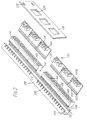
- Figure 1 shows the components of a single patch panel on the drop side patch.
- an array of these patch panels is used to make up the drop side patch.
- the panels are stacked one above the other in the array.
- the panel illustrated has the advantage that it can be stacked end-to-end as will be explained.
- the panel 10 comprises a mounting rail 12, an array of building interface connectors 14, an array of PCB mounted jacks 16 and a cover plate 18 (only partially shown). When assembled, pairs of patch connector jacks 19 are accessible through respective apertures 20 in the cover plate.
- the cover plate has at its corners mounting holes 22 which receive screws for connection to the drop side patch frame (not shown).
- the mounting rail 12 comprises a C-shaped channel having on the inside of each of its side walls a groove 24 which receives a corresponding rib 26 on the building interface connectors the building interface connectors may be clipped into position.
- the walls 28 carry a number of slots 30 which form wire outlet guides to facilitate the correct mounting of wires, (in the figure slots are only shown on one wall for ease of reference). Cables for connection to the building interface connectors may be inserted from the open end of the channel as shown by arrow 32.
- the building interface connectors 14 are insulation displacement contacts which each have upper and lower rows of insulation displacement contact blades 34, 36 which respectively connect with upper and lower faces of printed circuit boards (PCB's) 38.
- the rows of contacts 34, 36 are accessed by a slot 40 which extends right through the connector enabling the circuit board to be inserted from each side of the connector.
- cabling is introduced into the channel 12 as described. Individual wires are fed out from the cable through the relevant slot 30, over the outside of the connector 14, and into the displacement contact where they are terminated.
- slots 30 are arranged in groups of 14 along the channel with a gap between groups. This corresponds to the prior art arrangement of six eight wire connectors such as those used in Harmonicas (RTM) and presents an easily interpreted arrangement to the user.
- RTM Harmonicas
- IDCs insulation displacement connectors and contacts
- the connectors 14 are mounted on the rail 12 with the contacts at the front of the assembly.
- the IDCs can be wired from the front of the assembly, overcoming one of the disadvantages of the prior art. Maintenance is also easy as the IDCs are readily accessed by unscrewing the cover plate 18 and removing the printed circuit boards 38.
- the presentation of the fixed building wiring at the building interface connector is transformed to the Industry Standard for the service to be provided by the connection of a modular interface unit, here shown as PCB mounted jacks 16.
- the jacks are a pair of eight wire modular data connectors, although other numbers or standards of connector may be provided.
- one of the connectors 44 is wired to the upper terminals 42 of the edge connection printed circuit board and the connections of the other connector are wired, according to the relevant standard, to the lower terminals.
- the PCB is in position with the edge connectors received in the slot 40 of one of the insulation displacement connectors one of the connectors 44 will be connected to the upper row of contacts and the other to the lower row of contacts.
- the individual user positions are wired to respective ones of the upper and lower rows of contacts so that when a given PCB with associated connectors is inserted each connector is brought into contact with a user position in the building.
- a patch cord is then inserted into the connector and the other end of the cord is inserted into a desired connector on the system patch to connect the user position to a terminal.
- the building interface connector is an insulation displacement type connector
- other wire connection technologies could be used.
- the communication system could be used with optic fibre systems. In which case, optic fibre connection technology would replace the insulation displacement connectors.
- the interface between the sockets of the building interface connector and the connectors 44 are PCB edge type connectors.
- Other types of interface could be used and in particular other types of socket-plug interface.
- the building interface connector to comprise the plug and the interface with the connectors 44 to the patch cords to comprise the socket.
- the system need not be used solely in buildings.
- the patching system could easily be installed, for example, in ships or land vehicles.
- the configuration of the insulation displacement connectors or other interface connector with respect to its mounting has advantages which could be realised in different environments, for example in wall mounted sockets in telephone systems where a number of wires must be connected at individual user outlets.
- FIGs 2 and 3 an edge connector for use with the invention is illustrated.
- the construction of the patch panel is the same as that of Figure 1 and the same reference numerals are used with the addition of 100.
- the wiring connections to the various components are different as will be described.
- the printed circuit board used for insertion into the building interface connector shown in Figure 3 has been modified to produce a discontinuity 150 on one side of the edge contacts.
- a similar discontinuity may be introduced onto the other side.
- the effect of the discontinuity is such that on insertion into the slot 140 of a respective building interface contact only the front portion of the circuit board makes electrical contact with the interface connector 114.
- the front portion is connected by plated holes 152 to a corresponding track on the other face of the circuit board so that when in this first partially inserted position the upper and lower contacts of the building interface connector are connected together.
- the wiring of the drop patch panel of Figure 2 is modified from that of Figure 1 by wiring the computer port connections to the top (or bottom) row of insulation displacement contacts 134 and wiring the bottom (or top) row of contacts 136 to the user positions which correspond to the normal position of the terminals or telephones.
- the PCB 138 in its first partially inserted position the computer or telephone port connections will be connected directly to the terminals in their usual positional configuration.
- the PCBs are provided with a pair of apertures 154 which engage pips on the faces of slots 140 of the insulation displacement contacts.
- the apertures 154 could merely be detents and could, be located on the insulation displacement connectors with the pips on the PCB.
- connector arrays can be built up which corresponds to available cable sizes and wiring practices. Previously it has only been possible to obtain arrays in limited fixed pair counts. In addition end-to-end mounting of patch panels is possible by virtue of the arrangement of the contacts of the insulation displacement connectors in upper and lower rows. Moreover, the density of insulation displacement contacts can be chosen to match the density of patch field connectors 144 so avoiding unnecessary components and cost.
- the use of a through slot 40, 140 means that the circuit board could be introduced from either side so that if required, the interface connectors could be reversed to allow rear-face access to the insulation displacement contacts.
- the overall installation space is greatly reduced as the arrangement incorporates the secondary connection interface into the patch panel.
- the combined high-density of the connector system and the cable management within the mounting rails can allow up to twice as many connections per unit height as conventional systems.
- the system also lends itself to expansion; more, or more complex switching may be achieved by different arrangements of the circuit board interconnections or by introducing further discontinuities into the edge connectors whereby further insertion positions could be adopted.
Abstract
Description
- This invention relates to wiring systems particularly for data and voice communications systems. More specifically the invention is concerned with wiring distribution systems.
- In large scale wiring systems it is conventional to use a system of patch panels to connect an array of sub-stations to a main station. For example, a main frame computer in a building is required to communicate with a number of terminals located around the building. As the position of terminals is not usually fixed it is desirable to provide every room in the building and every potential user position within each room with a computer connection point. This will usually result in considerably more connection points than there are user ports on the computer. It is therefore necessary to provide a mechanical interface which allows ports to be connected to the user locations where terminals are to be installed.
- The mechanical interface used is a patch frame which is made of two arrays of patch panels, a system patch for the computer parts and a drop patch corresponding to the user positions. Computer ports are linked to selected ones of the user positions by flexible connections known as patch cords which extend between the respective locations on the system and drop patches of the port and user position being linked.
- Patch frame mechanical interfaces are used in a similar manner for telephone systems as well as data applications and although this specification describes the invention in terms of data systems it should be construed as being equally applicable to voice communication systems.
- Conventionally the system and drop patch arrays have used the same construction of patch panel in which, for example, groups of six eight wire connectors are connected in the panel to a single twenty five pair connector. The twenty five pair connector is then connected via a special cable assembly directly into the computer system to form the system patch. More recently, the groups of six eight wire connectors and the twenty five pair connector have been available as a single modular component. Such a component is sold by the present applicant under the trade mark Harmonica (RTM).
- Although the above structure is satisfactory for the system patch it is not so convenient for the drop patch. To be able to use the same type of panel for the drop patch a secondary connection interface is required. This is because the twenty five pair connector of each group of patch connectors receives a number of cables arranged in a different configuration, typically four pair cables. The secondary connection interface converts the four-pair cable format to twenty-five pair format. Conventionally this secondary interface is an insulation displacement connector system such as the AT & T 110 system or the Krone LSA Plus system.
- To reduce the work involved in installing the drop patch it has become usual to integrate the insulation displacement connector into the drop side patch panels which allows the building wiring to be terminated directly on to the rear face of the patch panels. Although various panels incorporating this feature are available commercially they all have the disadvantage that connection of wiring or maintenance requires access to the rear of the panel. As the panel is part of a patch frame this means that, in practice, access to the rear of the patch frame is required. As patch frames may be wall mounted and may be located in areas where there is restricted room for manoeuvre this disadvantage can cause acute problems.
- A further disadvantage of existing systems is that it is always necessary to use a patch cord to connect ports to user locations, even when the likelihood of the terminal being moved is remote.
- Some existing systems have attempted to eliminate the need for patch cords for terminals which are unlikely to be moved. This has been achieved by use of secondary mechanical switching devices or the use of special data jack connectors with switching contacts. Both have the disadvantage of being complex, awkward and expensive.
- The present invention aims to overcome the above mentioned disadvantages and to provide a patching system which is more convenient to install, maintain and use.
- Broadly, the invention resides in a system for connecting a source to at least one outlet in which the source is connected to a first connector which is mounted on a mounting means in such a way that connections between the source and the connector can be made from the side of the connector opposite to the side facing the mounting means.
- More specifically there is provided, a patching system comprising a system patch and a drop patch, the drop patch having at least one patch panel unit comprising a mounting rail carrying a plurality of first connectors each having a plurality of contacts for connecting conductors from the system patch to connectors for individual terminals, and a plurality of second connectors engageable with respective first connectors and carrying the connectors for individual terminals, the first connectors being mounted on the mounting rail such that the conductors from the system patch can be connected to the first connectors from the side of the first connectors which receives the second connectors.
- Preferably, the mounting rail comprises a channel, and the first connector is mounted in the channel with a space defined between the channel base and the connector. The cable is run along the channel base and individual conductors fed through slots in the channel wall. The conductors are then terminated at contacts on the face of the connector opposite to the channel base. This arrangement has the advantage that the cabling can be wired without requiring access to the rear side of the system.
- An embodiment of the invention will now be described, by way of example, and with reference to the accompanying drawings, in which:
- Figure 1 is an exploded view of a drop side patch panel embodying the invention;
- Figure 2 is a modified form of the embodiment of Figure 1 for use with a second edge connector; and
- Figure 3 is a partial view of an edge connector for use in the system of Figure 2.
- Figure 1 shows the components of a single patch panel on the drop side patch. In practice an array of these patch panels is used to make up the drop side patch. Conventionally the panels are stacked one above the other in the array. However, the panel illustrated has the advantage that it can be stacked end-to-end as will be explained.
- The
panel 10 comprises amounting rail 12, an array ofbuilding interface connectors 14, an array of PCB mountedjacks 16 and a cover plate 18 (only partially shown). When assembled, pairs ofpatch connector jacks 19 are accessible throughrespective apertures 20 in the cover plate. The cover plate has at itscorners mounting holes 22 which receive screws for connection to the drop side patch frame (not shown). - The
mounting rail 12 comprises a C-shaped channel having on the inside of each of its side walls agroove 24 which receives acorresponding rib 26 on the building interface connectors the building interface connectors may be clipped into position. Thewalls 28 carry a number ofslots 30 which form wire outlet guides to facilitate the correct mounting of wires, (in the figure slots are only shown on one wall for ease of reference). Cables for connection to the building interface connectors may be inserted from the open end of the channel as shown byarrow 32. - The
building interface connectors 14 are insulation displacement contacts which each have upper and lower rows of insulationdisplacement contact blades 34, 36 which respectively connect with upper and lower faces of printed circuit boards (PCB's) 38. The rows ofcontacts 34, 36 are accessed by aslot 40 which extends right through the connector enabling the circuit board to be inserted from each side of the connector. - To wire in the insulation displacement contacts cabling is introduced into the
channel 12 as described. Individual wires are fed out from the cable through therelevant slot 30, over the outside of theconnector 14, and into the displacement contact where they are terminated. - It will be appreciated that the
slots 30 are arranged in groups of 14 along the channel with a gap between groups. This corresponds to the prior art arrangement of six eight wire connectors such as those used in Harmonicas (RTM) and presents an easily interpreted arrangement to the user. - The individual insulation displacement connectors and contacts (IDCs) within those connectors are preferably those described in our co-pending International patent application number PCT/GB92/00998 claiming priority from British application 9112604.5 of 12 June 1991.
- As can be seen from Figure 1, the
connectors 14 are mounted on therail 12 with the contacts at the front of the assembly. Thus, with the mounting rail arranged in a frame the IDCs can be wired from the front of the assembly, overcoming one of the disadvantages of the prior art. Maintenance is also easy as the IDCs are readily accessed by unscrewing thecover plate 18 and removing the printedcircuit boards 38. - The presentation of the fixed building wiring at the building interface connector is transformed to the Industry Standard for the service to be provided by the connection of a modular interface unit, here shown as PCB mounted
jacks 16. Typically the jacks are a pair of eight wire modular data connectors, although other numbers or standards of connector may be provided. In the embodiment shown, one of theconnectors 44 is wired to theupper terminals 42 of the edge connection printed circuit board and the connections of the other connector are wired, according to the relevant standard, to the lower terminals. Thus, when the PCB is in position with the edge connectors received in theslot 40 of one of the insulation displacement connectors one of theconnectors 44 will be connected to the upper row of contacts and the other to the lower row of contacts. - The individual user positions are wired to respective ones of the upper and lower rows of contacts so that when a given PCB with associated connectors is inserted each connector is brought into contact with a user position in the building. A patch cord is then inserted into the connector and the other end of the cord is inserted into a desired connector on the system patch to connect the user position to a terminal.
- Various modifications to the patch panel described could be adopted. For example, it is not essential that the building interface connector is an insulation displacement type connector, other wire connection technologies could be used. It will be understood that the communication system could be used with optic fibre systems. In which case, optic fibre connection technology would replace the insulation displacement connectors.
- Similarly, it is not essential that the interface between the sockets of the building interface connector and the
connectors 44 are PCB edge type connectors. Other types of interface could be used and in particular other types of socket-plug interface. It would be possible for the building interface connector to comprise the plug and the interface with theconnectors 44 to the patch cords to comprise the socket. - Similarly, although described as building interface connectors, the system need not be used solely in buildings. The patching system could easily be installed, for example, in ships or land vehicles.
- Although described with respect to drop patching, the configuration of the insulation displacement connectors or other interface connector with respect to its mounting has advantages which could be realised in different environments, for example in wall mounted sockets in telephone systems where a number of wires must be connected at individual user outlets.
- Turning now to Figures 2 and 3 an edge connector for use with the invention is illustrated. The construction of the patch panel is the same as that of Figure 1 and the same reference numerals are used with the addition of 100. The wiring connections to the various components are different as will be described.
- Although, as described, it is desirable to be able to connect different user locations to different ports, there will be in most systems, a number of terminals or telephones which are unlikely to be moved. The embodiments of Figures 2 and 3 removes the need for patch cords for these terminals whilst retaining the possibility of future movement should the need arise.
- The printed circuit board used for insertion into the building interface connector shown in Figure 3 has been modified to produce a
discontinuity 150 on one side of the edge contacts. A similar discontinuity may be introduced onto the other side. The effect of the discontinuity is such that on insertion into theslot 140 of a respective building interface contact only the front portion of the circuit board makes electrical contact with theinterface connector 114. The front portion is connected by platedholes 152 to a corresponding track on the other face of the circuit board so that when in this first partially inserted position the upper and lower contacts of the building interface connector are connected together. - The wiring of the drop patch panel of Figure 2 is modified from that of Figure 1 by wiring the computer port connections to the top (or bottom) row of insulation displacement contacts 134 and wiring the bottom (or top) row of
contacts 136 to the user positions which correspond to the normal position of the terminals or telephones. Thus, with thePCB 138 in its first partially inserted position the computer or telephone port connections will be connected directly to the terminals in their usual positional configuration. - Further insertion of the PCB to a fully inserted second position in which the
discontinuity 150 extends beyond the IDCs breaks the contact between the upper and lower contact pairs of the IDCs. Thus, the port and the user location associated with that port under normal use appear at adjacent standardpatch field connectors 144, 144b. For example, theconnector 144 wired to therear end 156 of the contact strips on the upper side of the PCB will be connected to a computer port whereas connector 144b wired to the lower connectors will be connected to a user position. Patch cords can then be used between port and positionpatch field connectors 144 to establish connections as required. - To ensure firm location of the PCBs into the first and second position the PCBs are provided with a pair of
apertures 154 which engage pips on the faces ofslots 140 of the insulation displacement contacts. Theapertures 154 could merely be detents and could, be located on the insulation displacement connectors with the pips on the PCB. - The embodiment of the invention described has a number of advantages over the prior art discussed previously. In addition to overcoming the need for rear access and eliminating the need for patch cords under normal operating surfaces connector arrays can be built up which corresponds to available cable sizes and wiring practices. Previously it has only been possible to obtain arrays in limited fixed pair counts. In addition end-to-end mounting of patch panels is possible by virtue of the arrangement of the contacts of the insulation displacement connectors in upper and lower rows. Moreover, the density of insulation displacement contacts can be chosen to match the density of
patch field connectors 144 so avoiding unnecessary components and cost. - Although it is usually advantageous to have front access to the building interface connectors, the use of a through
slot - The use of a mounting rail which has an integral channel for building cables and wire outlet guides minimises the vertical spacing required between adjacent panels as no ties or restraints are needed for the cables. However, guide rings, spacers and other accessories for cable tidiness can easily be clipped into the grooves on the inside walls of the rails.
- As well as reducing vertical spacing, the overall installation space is greatly reduced as the arrangement incorporates the secondary connection interface into the patch panel. In addition the combined high-density of the connector system and the cable management within the mounting rails can allow up to twice as many connections per unit height as conventional systems. The system also lends itself to expansion; more, or more complex switching may be achieved by different arrangements of the circuit board interconnections or by introducing further discontinuities into the edge connectors whereby further insertion positions could be adopted.
Claims (2)
- A patching system for reconfigurably connecting a data or telecommunications source to selected ones of a plurality of user terminals comprising a system patch and a drop patch (10;110), the drop patch having at least one patch panel unit comprising a mounting rail (28;128) carrying a plurality of first connectors (14;114) each having a plurality of contacts (34;,36;134,136) for connecting conductors from the system patch to connectors for individual terminals, and a plurality of second connectors engageable with respective first connectors (14;114) and carrying the connectors for individual terminals, the first connectors being mounted on the mounting rail (28;128) such that the conductors from the system patch can be connected to the first connectors from the side of the first connectors which receives the second connectors.
- A system according to claim 1, wherein the mounting rail (28;128) comprises a channel, and the first connector is mounted in the channel with a space defined between the channel base and the connector.
Applications Claiming Priority (3)
| Application Number | Priority Date | Filing Date | Title |
|---|---|---|---|
| GB9115020 | 1991-07-05 | ||
| GB919115020A GB9115020D0 (en) | 1991-07-05 | 1991-07-05 | Electrical connection system |
| EP92914485A EP0593584B1 (en) | 1991-07-05 | 1992-07-06 | Electrical connection system |
Related Parent Applications (2)
| Application Number | Title | Priority Date | Filing Date |
|---|---|---|---|
| EP92914485.5 Division | 1992-07-06 | ||
| EP92914485A Division EP0593584B1 (en) | 1991-07-05 | 1992-07-06 | Electrical connection system |
Publications (2)
| Publication Number | Publication Date |
|---|---|
| EP0685905A2 true EP0685905A2 (en) | 1995-12-06 |
| EP0685905A3 EP0685905A3 (en) | 1997-11-19 |
Family
ID=10698227
Family Applications (2)
| Application Number | Title | Priority Date | Filing Date |
|---|---|---|---|
| EP95202155A Withdrawn EP0685905A3 (en) | 1991-07-05 | 1992-07-06 | Electrical connections systems |
| EP92914485A Expired - Lifetime EP0593584B1 (en) | 1991-07-05 | 1992-07-06 | Electrical connection system |
Family Applications After (1)
| Application Number | Title | Priority Date | Filing Date |
|---|---|---|---|
| EP92914485A Expired - Lifetime EP0593584B1 (en) | 1991-07-05 | 1992-07-06 | Electrical connection system |
Country Status (6)
| Country | Link |
|---|---|
| US (1) | US5492478A (en) |
| EP (2) | EP0685905A3 (en) |
| AU (3) | AU662008B2 (en) |
| DE (1) | DE69214289T2 (en) |
| GB (1) | GB9115020D0 (en) |
| WO (1) | WO1993001634A2 (en) |
Cited By (1)
| Publication number | Priority date | Publication date | Assignee | Title |
|---|---|---|---|---|
| WO2008025180A2 (en) * | 2006-09-01 | 2008-03-06 | Reichle & De-Massari Ag | Adapter and plug-in connection system |
Families Citing this family (28)
| Publication number | Priority date | Publication date | Assignee | Title |
|---|---|---|---|---|
| US5584728A (en) * | 1994-11-25 | 1996-12-17 | Hon Hai Precision Ind. Co., Ltd. | Modular connector assembly with variably positioned units |
| US5772448A (en) * | 1996-04-02 | 1998-06-30 | Compaq Computer Corporation | Edgecard circuit board |
| AU755171B2 (en) * | 1998-07-16 | 2002-12-05 | Reichle & De-Massari Ag | Set of contact blades in a multiple connector strip for cable connectors, and multiple connector strip |
| JP2000113920A (en) * | 1998-10-01 | 2000-04-21 | Mitsubishi Electric Corp | Module |
| YU70301A (en) * | 1999-04-06 | 2003-07-07 | Itracs Corporation | System for monitoring connection patern of data ports |
| SG74714A1 (en) * | 1999-04-06 | 2001-08-21 | Cablesoft Inc | A system for monitoring connection pattern of data ports |
| US6961675B2 (en) * | 2000-03-14 | 2005-11-01 | Itracs Corporation | System for monitoring connection pattern of data ports |
| DE10019451A1 (en) * | 2000-04-19 | 2001-10-25 | Scc Special Comm Cables Gmbh | Connection device and associated connector |
| US6676430B1 (en) * | 2000-05-23 | 2004-01-13 | Avaya Technology Corp. | Board mounted jack module |
| US6406332B1 (en) * | 2000-10-17 | 2002-06-18 | Dell Products, L.P. | Translating lockable card edge to card edge connector |
| DE10054258A1 (en) * | 2000-11-02 | 2002-05-16 | Vera Feislkorn | Device for distributing digital data between a server and network terminal devices e.g. computers, has connection elements arranged within housing directly on circuit board |
| US6358093B1 (en) | 2001-02-07 | 2002-03-19 | Adc Telecommunications, Inc. | Normal through jack and method |
| IL142157A (en) * | 2001-03-21 | 2008-03-20 | Rit Techn Ltd | Patch panel |
| US6761583B2 (en) * | 2001-06-01 | 2004-07-13 | Agilent Technologies, Inc. | Modular system interface apparatus |
| US6428351B1 (en) * | 2001-08-22 | 2002-08-06 | Mark Turner | Modular audio/power connector system |
| DE10205450A1 (en) * | 2002-02-08 | 2003-08-28 | Infineon Technologies Ag | Circuit carrier and manufacture of the same |
| US7641951B2 (en) * | 2004-05-01 | 2010-01-05 | Avery Dennison Corporation | Printing stock for use in printing composite signs, methods and apparatus for printing such signs, and methods for manufacturing such printing stock |
| JP4186920B2 (en) * | 2004-12-10 | 2008-11-26 | ソニー株式会社 | Accessories |
| US7679924B2 (en) * | 2005-10-17 | 2010-03-16 | Alcatel Lucent | Configurable chassis guidance system and method |
| US8769808B2 (en) * | 2005-10-17 | 2014-07-08 | Alcatel Lucent | Method for fixed and replaceable module architecture |
| DE102007026102B3 (en) * | 2007-06-05 | 2008-11-13 | Adc Gmbh | Connectors for printed circuit boards |
| DE102007026095A1 (en) * | 2007-06-05 | 2008-12-11 | Adc Gmbh | Earth comb, in particular for a connector for printed circuit boards |
| DE102007026096A1 (en) * | 2007-06-05 | 2008-12-11 | Adc Gmbh | Cable termination module |
| DE102007026094B4 (en) * | 2007-06-05 | 2023-05-11 | Tyco Electronics Services Gmbh | Contact element for a connector for printed circuit boards |
| DE102007026097B4 (en) * | 2007-06-05 | 2023-05-11 | Tyco Electronics Services Gmbh | Connectors for printed circuit boards |
| WO2011047281A1 (en) | 2009-10-16 | 2011-04-21 | Adc Telecommunications, Inc. | Managed connectivity in electrical systems and methods thereof |
| US20140024264A1 (en) * | 2012-07-18 | 2014-01-23 | Hsuan-Ho CHUNG | Portable electronic device |
| US10999929B2 (en) * | 2019-05-29 | 2021-05-04 | Quanta Computer Inc. | Expansion card interfaces for high-frequency signals and methods of making the same |
Family Cites Families (19)
| Publication number | Priority date | Publication date | Assignee | Title |
|---|---|---|---|---|
| NL6617684A (en) * | 1966-12-16 | 1968-06-17 | ||
| AU6377573A (en) * | 1973-01-02 | 1975-06-19 | Ranco Inc | Exhaust gas recirculating valve |
| US3850301A (en) * | 1973-03-14 | 1974-11-26 | Mc Donnell Douglas Corp | Mount for electrical junction blocks |
| US3951494A (en) * | 1974-11-14 | 1976-04-20 | Molex Incorporated | Electrical connector |
| US4017696A (en) * | 1975-12-31 | 1977-04-12 | Bell Telephone Laboratories, Incorporated | Initializing circuit |
| US4095866A (en) * | 1977-05-19 | 1978-06-20 | Ncr Corporation | High density printed circuit board and edge connector assembly |
| GB2060279A (en) * | 1979-09-24 | 1981-04-29 | Bunker Ramo | Communication system and means for interconnection of same |
| FR2518324A1 (en) * | 1981-12-11 | 1983-06-17 | Cit Alcatel | MULTI-COUPLING ELECTRICAL CONNECTOR AND MULTIPLE MEASURING CONNECTORS FOR ELECTRONIC EQUIPMENT CIRCUIT BOARDS MOUNTED IN CHASSIS BY APPLYING |
| US4556275A (en) * | 1983-06-23 | 1985-12-03 | Amp Incorporated | Electrical panelboard connector |
| JPS6243479U (en) * | 1985-09-02 | 1987-03-16 | ||
| JP2627908B2 (en) * | 1986-06-13 | 1997-07-09 | アンプ インコーポレーテッド | Receptacle assembly for LAN outlet and data connector used therefor |
| EP0278430A3 (en) * | 1987-02-06 | 1989-11-29 | Omron Tateisi Electronics Co. | Connection arrangement between control device and signal transmission device |
| DE3710896A1 (en) * | 1987-04-01 | 1988-10-20 | Krone Ag | DISTRIBUTION BOARD FOR TELECOMMUNICATION CABLES, IN PARTICULAR HOUSE ENTRANCE DISTRIBUTION BOARD |
| GB8711796D0 (en) * | 1987-05-19 | 1987-06-24 | Cambridge Computer Ltd | Microcomputers |
| US4789354A (en) * | 1987-09-14 | 1988-12-06 | Minnesota Mining And Manufacturing Company | Voice/data communication termination connector |
| US4824403A (en) * | 1988-01-15 | 1989-04-25 | Porta Systems Corp. | Telephone connector block for cradle type installtion |
| US4850899A (en) * | 1988-06-20 | 1989-07-25 | Maynard Scott D | Connector for interfacing a disk drive with a computer |
| DE3922431A1 (en) * | 1989-07-07 | 1991-01-10 | Siemens Ag | Distributor for disparate wire lines in telecommunication exchange - employs claw or screw terminals for wire ends on contact parts in common distributor moulding housing |
| US5037310A (en) * | 1989-12-06 | 1991-08-06 | Gespac, Inc. | Connector apparatus and method for distributed control modules used in computer networks |
-
1991
- 1991-07-05 GB GB919115020A patent/GB9115020D0/en active Pending
-
1992
- 1992-07-06 EP EP95202155A patent/EP0685905A3/en not_active Withdrawn
- 1992-07-06 WO PCT/GB1992/001220 patent/WO1993001634A2/en active IP Right Grant
- 1992-07-06 AU AU22553/92A patent/AU662008B2/en not_active Ceased
- 1992-07-06 DE DE69214289T patent/DE69214289T2/en not_active Expired - Fee Related
- 1992-07-06 EP EP92914485A patent/EP0593584B1/en not_active Expired - Lifetime
-
1994
- 1994-05-12 US US08/167,963 patent/US5492478A/en not_active Expired - Fee Related
-
1995
- 1995-08-22 AU AU30182/95A patent/AU679386B2/en not_active Ceased
- 1995-08-22 AU AU30183/95A patent/AU686416B2/en not_active Ceased
Non-Patent Citations (1)
| Title |
|---|
| None |
Cited By (3)
| Publication number | Priority date | Publication date | Assignee | Title |
|---|---|---|---|---|
| WO2008025180A2 (en) * | 2006-09-01 | 2008-03-06 | Reichle & De-Massari Ag | Adapter and plug-in connection system |
| WO2008025180A3 (en) * | 2006-09-01 | 2008-06-19 | Reichle & De Massari Fa | Adapter and plug-in connection system |
| US8100701B2 (en) | 2006-09-01 | 2012-01-24 | Reichle & De-Massari Ag | Adapter and plug-in connection system |
Also Published As
| Publication number | Publication date |
|---|---|
| AU662008B2 (en) | 1995-08-17 |
| AU2255392A (en) | 1993-02-11 |
| US5492478A (en) | 1996-02-20 |
| AU679386B2 (en) | 1997-06-26 |
| AU3018395A (en) | 1995-10-26 |
| EP0685905A3 (en) | 1997-11-19 |
| EP0593584A1 (en) | 1994-04-27 |
| AU686416B2 (en) | 1998-02-05 |
| EP0593584B1 (en) | 1996-10-02 |
| DE69214289D1 (en) | 1996-11-07 |
| WO1993001634A2 (en) | 1993-01-21 |
| DE69214289T2 (en) | 1997-04-24 |
| GB9115020D0 (en) | 1991-08-28 |
| WO1993001634A3 (en) | 1993-03-18 |
| AU3018295A (en) | 1995-10-26 |
Similar Documents
| Publication | Publication Date | Title |
|---|---|---|
| US5492478A (en) | Electrical connection system with alternatively positionable connector | |
| US6089892A (en) | Telecommunications cabling arrangement | |
| US4773867A (en) | Premise distribution cross connect apparatus | |
| US5647763A (en) | Multi-media cross connect system | |
| US7014495B2 (en) | Method and apparatus for zone cabling | |
| CA1118879A (en) | Modular termination system for communication lines | |
| US8758047B2 (en) | Port replication assembly with adapter cable and related methods of use | |
| US7503810B1 (en) | Board edge termination back-end connection assemblies and communications jacks including such assemblies | |
| WO2007092111A2 (en) | Service provider patch panel assembly | |
| US6974911B2 (en) | Modular wiring system | |
| EP0552022B1 (en) | Jack cluster with offset mounting posts | |
| US4678251A (en) | Modular installation system for data cable interfacing | |
| US6186808B1 (en) | High density high performance telecommunications/data link and connector with tap and contact displacement assembly | |
| CA2216679A1 (en) | Transition adapter for conductor cable | |
| US4753610A (en) | Connectorized terminal block | |
| GB2286731A (en) | Electrical connection system | |
| US5741157A (en) | Raceway system with transition adapter | |
| CA1159976A (en) | Low cost user reprogrammable communication system | |
| CA1253611A (en) | Modular cable interconnection apparatus |
Legal Events
| Date | Code | Title | Description |
|---|---|---|---|
| PUAI | Public reference made under article 153(3) epc to a published international application that has entered the european phase |
Free format text: ORIGINAL CODE: 0009012 |
|
| 17P | Request for examination filed |
Effective date: 19950823 |
|
| AC | Divisional application: reference to earlier application |
Ref document number: 593584 Country of ref document: EP |
|
| AK | Designated contracting states |
Kind code of ref document: A2 Designated state(s): BE DE FR GB IT NL |
|
| PUAL | Search report despatched |
Free format text: ORIGINAL CODE: 0009013 |
|
| AK | Designated contracting states |
Kind code of ref document: A3 Designated state(s): BE DE FR GB IT NL |
|
| 17Q | First examination report despatched |
Effective date: 19981007 |
|
| STAA | Information on the status of an ep patent application or granted ep patent |
Free format text: STATUS: THE APPLICATION IS DEEMED TO BE WITHDRAWN |
|
| 18D | Application deemed to be withdrawn |
Effective date: 19990420 |