EP0677765B1 - Optical waveguide device - Google Patents
Optical waveguide device Download PDFInfo
- Publication number
- EP0677765B1 EP0677765B1 EP95108382A EP95108382A EP0677765B1 EP 0677765 B1 EP0677765 B1 EP 0677765B1 EP 95108382 A EP95108382 A EP 95108382A EP 95108382 A EP95108382 A EP 95108382A EP 0677765 B1 EP0677765 B1 EP 0677765B1
- Authority
- EP
- European Patent Office
- Prior art keywords
- optical waveguide
- electrodes
- semiconductive layer
- pair
- layer
- Prior art date
- Legal status (The legal status is an assumption and is not a legal conclusion. Google has not performed a legal analysis and makes no representation as to the accuracy of the status listed.)
- Expired - Lifetime
Links
Images


Classifications
-
- G—PHYSICS
- G02—OPTICS
- G02F—OPTICAL DEVICES OR ARRANGEMENTS FOR THE CONTROL OF LIGHT BY MODIFICATION OF THE OPTICAL PROPERTIES OF THE MEDIA OF THE ELEMENTS INVOLVED THEREIN; NON-LINEAR OPTICS; FREQUENCY-CHANGING OF LIGHT; OPTICAL LOGIC ELEMENTS; OPTICAL ANALOGUE/DIGITAL CONVERTERS
- G02F1/00—Devices or arrangements for the control of the intensity, colour, phase, polarisation or direction of light arriving from an independent light source, e.g. switching, gating or modulating; Non-linear optics
- G02F1/01—Devices or arrangements for the control of the intensity, colour, phase, polarisation or direction of light arriving from an independent light source, e.g. switching, gating or modulating; Non-linear optics for the control of the intensity, phase, polarisation or colour
- G02F1/03—Devices or arrangements for the control of the intensity, colour, phase, polarisation or direction of light arriving from an independent light source, e.g. switching, gating or modulating; Non-linear optics for the control of the intensity, phase, polarisation or colour based on ceramics or electro-optical crystals, e.g. exhibiting Pockels effect or Kerr effect
- G02F1/035—Devices or arrangements for the control of the intensity, colour, phase, polarisation or direction of light arriving from an independent light source, e.g. switching, gating or modulating; Non-linear optics for the control of the intensity, phase, polarisation or colour based on ceramics or electro-optical crystals, e.g. exhibiting Pockels effect or Kerr effect in an optical waveguide structure
-
- G—PHYSICS
- G02—OPTICS
- G02F—OPTICAL DEVICES OR ARRANGEMENTS FOR THE CONTROL OF LIGHT BY MODIFICATION OF THE OPTICAL PROPERTIES OF THE MEDIA OF THE ELEMENTS INVOLVED THEREIN; NON-LINEAR OPTICS; FREQUENCY-CHANGING OF LIGHT; OPTICAL LOGIC ELEMENTS; OPTICAL ANALOGUE/DIGITAL CONVERTERS
- G02F1/00—Devices or arrangements for the control of the intensity, colour, phase, polarisation or direction of light arriving from an independent light source, e.g. switching, gating or modulating; Non-linear optics
- G02F1/01—Devices or arrangements for the control of the intensity, colour, phase, polarisation or direction of light arriving from an independent light source, e.g. switching, gating or modulating; Non-linear optics for the control of the intensity, phase, polarisation or colour
- G02F1/21—Devices or arrangements for the control of the intensity, colour, phase, polarisation or direction of light arriving from an independent light source, e.g. switching, gating or modulating; Non-linear optics for the control of the intensity, phase, polarisation or colour by interference
- G02F1/225—Devices or arrangements for the control of the intensity, colour, phase, polarisation or direction of light arriving from an independent light source, e.g. switching, gating or modulating; Non-linear optics for the control of the intensity, phase, polarisation or colour by interference in an optical waveguide structure
-
- G—PHYSICS
- G02—OPTICS
- G02F—OPTICAL DEVICES OR ARRANGEMENTS FOR THE CONTROL OF LIGHT BY MODIFICATION OF THE OPTICAL PROPERTIES OF THE MEDIA OF THE ELEMENTS INVOLVED THEREIN; NON-LINEAR OPTICS; FREQUENCY-CHANGING OF LIGHT; OPTICAL LOGIC ELEMENTS; OPTICAL ANALOGUE/DIGITAL CONVERTERS
- G02F1/00—Devices or arrangements for the control of the intensity, colour, phase, polarisation or direction of light arriving from an independent light source, e.g. switching, gating or modulating; Non-linear optics
- G02F1/01—Devices or arrangements for the control of the intensity, colour, phase, polarisation or direction of light arriving from an independent light source, e.g. switching, gating or modulating; Non-linear optics for the control of the intensity, phase, polarisation or colour
- G02F1/21—Devices or arrangements for the control of the intensity, colour, phase, polarisation or direction of light arriving from an independent light source, e.g. switching, gating or modulating; Non-linear optics for the control of the intensity, phase, polarisation or colour by interference
- G02F1/225—Devices or arrangements for the control of the intensity, colour, phase, polarisation or direction of light arriving from an independent light source, e.g. switching, gating or modulating; Non-linear optics for the control of the intensity, phase, polarisation or colour by interference in an optical waveguide structure
- G02F1/2255—Devices or arrangements for the control of the intensity, colour, phase, polarisation or direction of light arriving from an independent light source, e.g. switching, gating or modulating; Non-linear optics for the control of the intensity, phase, polarisation or colour by interference in an optical waveguide structure controlled by a high-frequency electromagnetic component in an electric waveguide structure
-
- G—PHYSICS
- G02—OPTICS
- G02F—OPTICAL DEVICES OR ARRANGEMENTS FOR THE CONTROL OF LIGHT BY MODIFICATION OF THE OPTICAL PROPERTIES OF THE MEDIA OF THE ELEMENTS INVOLVED THEREIN; NON-LINEAR OPTICS; FREQUENCY-CHANGING OF LIGHT; OPTICAL LOGIC ELEMENTS; OPTICAL ANALOGUE/DIGITAL CONVERTERS
- G02F2201/00—Constructional arrangements not provided for in groups G02F1/00 - G02F7/00
- G02F2201/06—Constructional arrangements not provided for in groups G02F1/00 - G02F7/00 integrated waveguide
- G02F2201/066—Constructional arrangements not provided for in groups G02F1/00 - G02F7/00 integrated waveguide channel; buried
-
- G—PHYSICS
- G02—OPTICS
- G02F—OPTICAL DEVICES OR ARRANGEMENTS FOR THE CONTROL OF LIGHT BY MODIFICATION OF THE OPTICAL PROPERTIES OF THE MEDIA OF THE ELEMENTS INVOLVED THEREIN; NON-LINEAR OPTICS; FREQUENCY-CHANGING OF LIGHT; OPTICAL LOGIC ELEMENTS; OPTICAL ANALOGUE/DIGITAL CONVERTERS
- G02F2203/00—Function characteristic
- G02F2203/21—Thermal instability, i.e. DC drift, of an optical modulator; Arrangements or methods for the reduction thereof
Definitions
- the present invention relates to an optical waveguide device, and more particularly to an optical waveguide device such as a modulator, switch, distributor, or the like, used in optical communication apparatus.
- a typical optical waveguide device used in an optical switch, an optical modulator, or the like is constituted such that an electric field is applied to an optical waveguide formed on a surface of a substrate consisting of electrooptical crystal such as lithium niobate (LiNbO 3 ), or the like, so as to change a refractive index, and thus switching or phase modulation of a light signal traveling through the optical waveguide can be carried out.
- electrooptical crystal such as lithium niobate (LiNbO 3 ), or the like
- an optical waveguide device typically includes an optical waveguide formed on a surface of a substrate having an electrooptical effect and a pair of electrodes formed on corresponding regions above the optical waveguide and receiving a driving electric signal thereacross.
- a distribution of electric field occurring in a vicinity of the optical waveguide by an application of the electric signal is greatly changed in accordance with a change in a frequency of the electric signal.
- a Mach-Zehnder type modulator As an example of the optical waveguide device, a Mach-Zehnder type modulator is well known.
- a modulator of this type includes at least an optical waveguide formed on a surface of a Z-cut LiNbO 3 substrate and a pair of asymmetrical electrodes formed on corresponding regions above the optical waveguide.
- charges collected on the surface of the LiNbO 3 substrate by the pyroelectric effect act on the asymmetrical structure of the electrodes and thus a disadvantage occurs in that the distribution of charges is made uneven and an adverse influence is exerted on characteristics of the device.
- Both JP-A-62 073 207 and JP-A-1 302 325 disclose an optical waveguide device in which at least two metal electrodes are formed on a buffer layer overlying a LiNbO 3 substrate.
- optical waveguide device capable of suppressing a DC drift thereof to effectively compensate for fluctuation in operational characteristics due to the DC drift, stress, or the like.
- an optical waveguide device in which a third electrode other than the pair of driving electrodes is provided on a region spaced by a predetermined distance from the pair of driving electrodes formed on corresponding regions above the optical waveguide.
- the third electrode may receive a DC or low frequency voltage, or may be grounded under predetermined layout conditions of each electrode.
- a semiconductive layer of, e.g., silicon (Si) is formed on a buffer layer so as to make uniform a distribution of charges occurring in the vicinity of the surface of the optical waveguide.
- a potential on the semiconductive (Si) region on the outside of the signal line electrode i.e. on the opposite side of the grounding electrode
- the silicon (Si) layer acts as a conductor in a low frequency band.
- a third electrode may be provided on the outside of the signal line electrode, i.e. on the opposite side of the grounding electrode.
- the third electrode on a region spaced from the signal line electrode by a sufficient distance, it is possible to reduce the influence exerted on the characteristic impedance of the traveling wave electrode.
- the applicants propose the use of a semiconductor layer having a relatively low resistance in place of a conductor as the third electrode, thereby gaining the same effect as above and further reducing the influence exerted on the characteristic impedance.
- the third electrode may receive a voltage signal.
- more effective advantages can be obtained. Namely, by applying a DC or low frequency voltage to the third electrode, it is possible to compensate for a fluctuation in operational characteristics occurring due to a DC drift, mechanical stress, or the like.
- a semiconductor layer consisting of material having a relatively high resistance, e.g. silicon (Si), is formed close to the signal line electrode.
- the semiconductor layer may receive a voltage directly from an external power source, or may receive the voltage via a conductor layer, which is formed on the semiconductor layer at a position spaced from the signal line electrode by a sufficient distance such that its presence does not greatly affect a characteristic impedance of the traveling wave electrode.
- the semiconductive layer functions as a conductor with respect to a low frequency voltage and functions as a dielectric with respect to a high frequency voltage. Accordingly, the presence of the semiconductive layer has less influence on the characteristic impedance in the high frequency band of the applied voltage.
- another semiconductive layer may be formed all over the buffer layer so as to improve temperature characteristics. In this case, by decreasing the thickness of the semiconductive layer in the vicinity of the signal line electrode and concentrating the electric field on the thinly formed portion, it is possible to realise the same effect as above.
- Electrodes constituting optical modulators, optical switches, or the like are formed to have a low resistance and thus enable a high speed operation.
- a material having a high electric conductivity such as copper (Cu), gold (Au), or the like, and increase the thickness of the electrode.
- a material having a relatively high resistance such as a silicon (Si) layer is adjacent to the material having a high electric conductivity, it functions in different phases in accordance with the selection of the resistance value. Namely, when a DC or low frequency voltage is applied to the signal line electrode, the silicon (Si) layer is kept in a state of equal potential in the same manner as the conductor (electrode).
- a pair of electrodes for a traveling wave are normally employed.
- a semiconductive layer comprised of silicon (Si) is formed between the pair of electrodes and the buffer layer.
- the semiconductive layer is separated into two regions in the center of the corresponding region thereof between the electrode for signal line and the electrode for grounding.
- an optical waveguide device comprising: an optical waveguide formed on a surface of a substrate having an electro-optical effect; a pair of electrodes operatively connected and arranged to receive a driving electric signal thereacross; a buffer layer formed all over the said surface of said substrate including the optical waveguide; and a semiconductive layer formed between the buffer layer and the pair of electrodes, a part of the said semiconductive layer which corresponds to the gap between the pair of electrodes being of reduced or zero thickness; wherein a change in frequency of the driving electric signal applied across the pair of electrodes when the device is in use brings about a corresponding change in a distribution of an electric field which occurs in the vicinity of the optical waveguide, and wherein, when a low frequency electric signal is applied to the pair of electrodes, the electric field is concentrated on the said part of the said semiconductive layer.
- an optical waveguide device comprising: an optical waveguide formed on a surface of a substrate having an electro-optical effect; a pair of electrodes operatively connected and arranged to receive a driving electric signal thereacross; a buffer layer formed all over said surface of said substrate including the optical waveguide; and a first semiconductive layer, formed between the buffer layer and the pair of electrodes, and a second semiconductive layer, formed between the first semiconductive layer and a signal line electrode of the pair of electrodes, the second semiconductive layer having a specific resistance different from that of the first semiconductive layer and having a broader width than that of the signal line electrode; wherein a change in frequency of a driving electric signal applied therebetween when the device is in use brings about a corresponding change in a distribution of an electric field which occurs in the vicinity of the optical waveguide.
- Figures 1A and 1B show a structure of a prior art Mach-Zehnder type modulator. Note, Fig. 1B shows a sectional structure along the line A-A' in Fig. 1A. The illustrated structure shows an example using asymmetrical electrodes for a traveling wave.
- reference 1 denotes a Z-cut LiNbO 3 substrate and reference 2 denotes an optical waveguide including two-forked optical waveguides 2a and 2b.
- the optical waveguide 2 (2a, 2b) is formed by effecting a striplike patterning of a Titanium (Ti)-deposited layer formed on a surface of the substrate 1 and then effecting a thermal diffusion of the Titanium into the substrate 1.
- the optical waveguide 2 (2a, 2b) has a larger refractive index than that of the substrate 1.
- a dielectric buffer layer 3 is formed between the electrodes 5, 6 and the optical waveguide 2.
- the buffer layer 3 is translucent and has a smaller refractive index than that of the optical waveguide 2.
- the buffer layer 3 is comprised of, for example, silicon dioxide (SiO 2 ).
- the dielectric layer 3 electrically functions as a capacitance containing relatively high resistance material.
- a disadvantage occurs in that charges collected on the surface of the substrate by the pyroelectric effect act on the asymmetrical structure of the electrodes formed on the buffer layer and thus an uneven distribution of charges is formed, which has an adverse influence on characteristics of the optical waveguide device.
- a semiconductive layer 4 comprised of, for example, silicon (Si) is formed between the buffer layer 3 and the electrodes 5, 6 and all over the buffer layer 3 (see Fig. 1B).
- the optical waveguide 2 is formed by diffusing the Titanium with high temperature into the LiNbO 3 substrate 1, its resistance, dielectric constant and capacitance are different from those of the bulk portion of the substrate 1. Additionally, a resistance of the surface of the LiNbO 3 substrate 1 is different from that of the bulk portion thereof due to the diffusing process.
- the electrical equivalent circuit also becomes complicated. As a result, a problem occurs in that a DC component of an electric signal applied across the electrodes 5, 6 greatly changes an application manner of the electric field with a long-term time constant in accordance with the process conditions and the optical response characteristics are also accordingly changed. Namely, a DC drift is caused.
- a drawback occurs in that the device is brought to an electrically open state seen from the power source and thus an adverse influence is exerted on the operation of the power source.
- a disadvantage also occurs in that an available frequency band of the power source is limited in dependence on the capacity thereof.
- a drawback occurs in that a characteristic impedance of the traveling wave signal line electrode fluctuates and thus it is impossible to satisfactorily carry out the modulation operation.
- a structure or means other than the electrodes provided for switching or modulation needs to be provided for suppressing a DC drift and compensating for a fluctuation in operational characteristics due to the DC drift, stress, or the like.
- the structure illustrated in Figs. 1A and 1B may be modified in accordance with the first aspect of the present invention so as to have a semiconductive layer (4a, 4b) formed between the buffer layer 3 and the electrodes 5 and 6.
- the semiconductive layer is comprised of silicon (Si) and has a thickness of approximately 0.2 ⁇ m, and is separated into two regions 4a and 4b in the center of the corresponding region thereof between the electrodes 5 and 6.
- the gap between the separated portions 4a, 4b, indicated by reference P, is selected to be 1 to 4 ⁇ m.
- each semiconductive layer 4a, 4b has a broader width than that of the corresponding electrode 5, 6.
- a specific resistance of the semiconductive layer (4a, 4b) can be designed and selected over a wide range from 0.001 to 100000 ⁇ m.
- the present optical modulator is used in a frequency of 5 to 6 MHz or more, the specific resistance is preferably selected to be 100 ⁇ m.
- the specific resistance is altered in accordance with a thickness of each layer, a layer-to-layer distance, a distance between each electrode, and the like.
- Figure 3 shows a first modification of the embodiment shown in Figs. 2A and 2B.
- the semiconductive layer 4a is formed only in the vicinity of the electrode for signal line 5. Since the width of the semiconductive layer 4a formed under the electrode 5 can be arbitrarily designed and selected, it is possible to realize better frequency characteristics.
- Figure 4 shows a structure of a second modification.
- a semiconductive layer 4c comprised of silicon (Si) is formed between the buffer layer 3 and the electrodes 5 and 6 and all over the buffer layer 3.
- the semiconductive layer 4c has a thinly formed portion Q in the center of the corresponding region thereof between the electrodes 5 and 6.
- Figure 5 shows a structure of a third modification, which is a combination of the example of Fig. 3 and the example of Fig. 4.
- the semiconductive layer 4c is formed only in the vicinity of the signal line electrode 5, it is possible to realize better frequency characteristics as in the example of Fig. 3.
- the structure illustrated in Figs. 1A and 1B may be modified alternatively in accordance with the second aspect of the present invention so as to have a first semiconductive layer 4 and a second semiconductive layer 9a provided in place of the separated semiconductive layers 4a, 4b shown in Figs. 2A and 2B.
- the semiconductive layer 4 is comprised of silicon (Si) and formed between the buffer layer 3 and the electrode 6 and all over the buffer layer 3.
- the semiconductive layer 9a is comprised of silicon (Si) and formed between the semiconductive layer 4 and the electrode 5.
- the semiconductive layer 9a has a specific resistance different from that of the semiconductive layer 4 and has a broader width than that of the corresponding electrode 5.
- the electric field in the vicinity of the optical waveguide 2b beneath the grounding electrode 6 is relatively weak. Therefore, even if a DC electric field is concentrated on the region between the electrodes 5 and 6, it is possible to suppress the influence exerted on the refractive index of the optical waveguide 2b beneath the electrode 6 and thus gain the same effect as above.
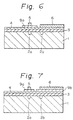
- Figure 7 shows a structure of a first modification, which is an improvement of the example of Fig. 6.
- a semiconductive layer 9b comprised of silicon (Si) is added to the structure shown in Fig. 6.
- the semiconductive layer 9b is formed between the semiconductive layer 4 and the electrode 6.
- the semiconductive layer 9b has a specific resistance different from that of the semiconductive layers 4, 9a and has a broader width than that of the corresponding electrode 6. Since the present device has a number of design parameters, it is possible to design and optimize the device more effectively and thus gain a better effect.
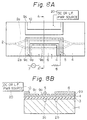
- Figures 8A and 8B show a structure of a second modification.
- the structure of Figs. 8A and 8B has a semiconductive layer 9c, comprising silicon (Si), on which a third electrode 10 is formed, the layer 9c being separated from the layer 9a in a region between the electrodes 5 and 10.
- the semiconductive layer 9c has a specific resistance different from that of the semiconductive layer 4 and has a broader width than that of the electrode 10. According to this structure, it is possible to suppress a DC drift of the device and thus effectively compensate for a fluctuation in operational characteristics due to the DC drift, stress, or the like.
- the present invention is applicable to other optical waveguide devices such as optical switches, or the like. Also, the present invention can be applied to an optical waveguide device to which a low frequency signal and a high frequency signal are fed independently.
Landscapes
- Physics & Mathematics (AREA)
- Nonlinear Science (AREA)
- General Physics & Mathematics (AREA)
- Optics & Photonics (AREA)
- Chemical & Material Sciences (AREA)
- Engineering & Computer Science (AREA)
- Ceramic Engineering (AREA)
- Crystallography & Structural Chemistry (AREA)
- Optical Modulation, Optical Deflection, Nonlinear Optics, Optical Demodulation, Optical Logic Elements (AREA)
- Optical Integrated Circuits (AREA)
Description
- The present invention relates to an optical waveguide device, and more particularly to an optical waveguide device such as a modulator, switch, distributor, or the like, used in optical communication apparatus.
- A typical optical waveguide device used in an optical switch, an optical modulator, or the like, is constituted such that an electric field is applied to an optical waveguide formed on a surface of a substrate consisting of electrooptical crystal such as lithium niobate (LiNbO3), or the like, so as to change a refractive index, and thus switching or phase modulation of a light signal traveling through the optical waveguide can be carried out.
- In particular, an optical waveguide device typically includes an optical waveguide formed on a surface of a substrate having an electrooptical effect and a pair of electrodes formed on corresponding regions above the optical waveguide and receiving a driving electric signal thereacross. A distribution of electric field occurring in a vicinity of the optical waveguide by an application of the electric signal is greatly changed in accordance with a change in a frequency of the electric signal.
- As an example of the optical waveguide device, a Mach-Zehnder type modulator is well known. A modulator of this type includes at least an optical waveguide formed on a surface of a Z-cut LiNbO3 substrate and a pair of asymmetrical electrodes formed on corresponding regions above the optical waveguide. In such a structure, charges collected on the surface of the LiNbO3 substrate by the pyroelectric effect act on the asymmetrical structure of the electrodes and thus a disadvantage occurs in that the distribution of charges is made uneven and an adverse influence is exerted on characteristics of the device.
- Also, since the distribution of resistance, dielectric constant and capacitance of each portion of the structure or partial fine structure is delicately changed in accordance with the process conditions, the electrical equivalent circuit accordingly becomes complicated. This results in a problem in that a direct current (DC) component of an electric signal applied across the electrodes greatly changes an application manner of the electric field with a long-term time constant and the optical response is also accordingly changed. This phenomenon is called a DC drift.
- Both JP-A-62 073 207 and JP-A-1 302 325 disclose an optical waveguide device in which at least two metal electrodes are formed on a buffer layer overlying a LiNbO3 substrate.
- It is therefore desirable to provide an optical waveguide device capable of suppressing a DC drift thereof to effectively compensate for fluctuation in operational characteristics due to the DC drift, stress, or the like.
- In the applicant's co-pending European patent application No. 91301729.9 there is proposed an optical waveguide device in which a third electrode other than the pair of driving electrodes is provided on a region spaced by a predetermined distance from the pair of driving electrodes formed on corresponding regions above the optical waveguide. The third electrode may receive a DC or low frequency voltage, or may be grounded under predetermined layout conditions of each electrode.
- In an optical waveguide device formed on an electrooptical crystal substrate having a pyroelectric effect, it is preferable that a semiconductive layer of, e.g., silicon (Si) is formed on a buffer layer so as to make uniform a distribution of charges occurring in the vicinity of the surface of the optical waveguide. In this case, in a structure having a narrow signal line electrode and a wide grounding electrode, a potential on the semiconductive (Si) region on the outside of the signal line electrode (i.e. on the opposite side of the grounding electrode) is uniformly made equal because the silicon (Si) layer acts as a conductor in a low frequency band. As a result, a drawback arises in that the electric field to be concentrated on the vicinity of the signal line electrode is dispersed into the outside semiconductive (Si) region and thus it is not effectively applied to the optical waveguide.
- To cope with this drawback, a third electrode may be provided on the outside of the signal line electrode, i.e. on the opposite side of the grounding electrode. By this structure, it is possible to cause a voltage drop in proportion to the distance between the signal line electrode and the third electrode and thus concentrate the dispersed electric field on the vicinity of the signal line electrode. Also, by suitably changing the thickness of the silicon (Si) layer between the signal line electrode and the third electrode, it is possible to change a distribution of resistance therebetween to regulate a distribution of the voltage drop and thus concentrate the electric field more effectively. On the other hand, when a high frequency electric signal is applied to the pair of driving electrodes, charges in the silicon (Si) layer cannot follow a change in the high frequency electric signal and thus the semiconductive layer functions as a dielectric. Also, by disposing the third electrode on a region spaced from the signal line electrode by a sufficient distance, it is possible to reduce the influence exerted on the characteristic impedance of the traveling wave electrode. In the afore-mentioned co-pending application the applicants propose the use of a semiconductor layer having a relatively low resistance in place of a conductor as the third electrode, thereby gaining the same effect as above and further reducing the influence exerted on the characteristic impedance.
- Although the above structure premises that the third electrode is grounded, the third electrode may receive a voltage signal. In this case, more effective advantages can be obtained. Namely, by applying a DC or low frequency voltage to the third electrode, it is possible to compensate for a fluctuation in operational characteristics occurring due to a DC drift, mechanical stress, or the like. In this case, it is preferable that a semiconductor layer consisting of material having a relatively high resistance, e.g. silicon (Si), is formed close to the signal line electrode. The semiconductor layer may receive a voltage directly from an external power source, or may receive the voltage via a conductor layer, which is formed on the semiconductor layer at a position spaced from the signal line electrode by a sufficient distance such that its presence does not greatly affect a characteristic impedance of the traveling wave electrode. By applying the voltage directly or indirectly to the semiconductor layer, it is possible to change a refractive index of the optical waveguide beneath the signal line electrode and thus compensate for a fluctuation in operational characteristics. In this case, the semiconductive layer functions as a conductor with respect to a low frequency voltage and functions as a dielectric with respect to a high frequency voltage. Accordingly, the presence of the semiconductive layer has less influence on the characteristic impedance in the high frequency band of the applied voltage. Also, another semiconductive layer may be formed all over the buffer layer so as to improve temperature characteristics. In this case, by decreasing the thickness of the semiconductive layer in the vicinity of the signal line electrode and concentrating the electric field on the thinly formed portion, it is possible to realise the same effect as above.
- In the present application the applicants propose an alternative solution which is an improvement of a conventional Mach-Zehnder type optical waveguide device and which is based on the principle described below.
- Electrodes constituting optical modulators, optical switches, or the like, are formed to have a low resistance and thus enable a high speed operation. To this end, it is preferabe to use a material having a high electric conductivity such as copper (Cu), gold (Au), or the like, and increase the thickness of the electrode. Where a material having a relatively high resistance such as a silicon (Si) layer is adjacent to the material having a high electric conductivity, it functions in different phases in accordance with the selection of the resistance value. Namely, when a DC or low frequency voltage is applied to the signal line electrode, the silicon (Si) layer is kept in a state of equal potential in the same manner as the conductor (electrode). Contrary to this, where the frequency of the signal propagating on the signal line electrode is gradually increased, charges in the silicon (Si) region cannot follow a high speed change in the signal, and thus, a region in which charges can follow the high speed change in the signal is gradually limited to the vicinity of the conductor (electrode). In other words, an effective shape of the electrode is greatly changed between the low frequency band and the high frequency band. By utilizing the change in the effective shape of the electrode, it is possible to constitute a device having various functions.
- To realize a high speed switching or modulation, a pair of electrodes for a traveling wave are normally employed. According to an improved structure, a semiconductive layer comprised of silicon (Si) is formed between the pair of electrodes and the buffer layer. The semiconductive layer is separated into two regions in the center of the corresponding region thereof between the electrode for signal line and the electrode for grounding. By this constitution, an electric field by a DC or low frequency component of the applied signal is concentrated on the separated portion and a component of the electric field in the vicinity of the optical waveguide is weakened. Accordingly, even if the DC or low frequency component is changed due to a DC drift, it is possible to suppress a fluctuation in operational characteristics. On the other hand, where a high frequency electric signal is applied to the pair of electrodes, charges in the silicon (Si) layer cannot follow a change in the high frequency electric signal and thus the silicon layer functions as a dielectric. In this case, since the electric field is applied across the pair of electrodes, it effectively acts on the optical waveguide.
- Also, even in the case that a thinly formed conductive layer is substituted for the above-mentioned semiconductive layer, it is possible to realize the same effect as above. This is because even the conductor has a larger volume resistivity than zero and the resistance value is increased with a decrease in the thickness of the conductive layer.
- Thus, according to a first aspect of the present invention there is provided an optical waveguide device comprising: an optical waveguide formed on a surface of a substrate having an electro-optical effect; a pair of electrodes operatively connected and arranged to receive a driving electric signal thereacross; a buffer layer formed all over the said surface of said substrate including the optical waveguide; and a semiconductive layer formed between the buffer layer and the pair of electrodes, a part of the said semiconductive layer which corresponds to the gap between the pair of electrodes being of reduced or zero thickness; wherein a change in frequency of the driving electric signal applied across the pair of electrodes when the device is in use brings about a corresponding change in a distribution of an electric field which occurs in the vicinity of the optical waveguide, and wherein, when a low frequency electric signal is applied to the pair of electrodes, the electric field is concentrated on the said part of the said semiconductive layer.
- According to a second aspect of the present invention there is provided an optical waveguide device comprising: an optical waveguide formed on a surface of a substrate having an electro-optical effect; a pair of electrodes operatively connected and arranged to receive a driving electric signal thereacross; a buffer layer formed all over said surface of said substrate including the optical waveguide; and a first semiconductive layer, formed between the buffer layer and the pair of electrodes, and a second semiconductive layer, formed between the first semiconductive layer and a signal line electrode of the pair of electrodes, the second semiconductive layer having a specific resistance different from that of the first semiconductive layer and having a broader width than that of the signal line electrode; wherein a change in frequency of a driving electric signal applied therebetween when the device is in use brings about a corresponding change in a distribution of an electric field which occurs in the vicinity of the optical waveguide.
- Reference will now be made, by way of example, to the accompanying drawings, in which:
- Figs. 1A and 1B show plan and sectional views, respectively, of a structure of a prior art Mach-Zehnder type modulator;
- Figs. 2A and 2B show plan and sectional views, respectively, of an optical waveguide device (optical modulator) embodying the first aspect of the present invention;
- Fig. 3 shows a sectional view of a first modification of the structure shown in Figs. 2A and 2B;
- Fig. 4 shows a sectional view of a second modification of the structure shown in Figs. 2A and 2B;
- Fig. 5 shows a sectional view of a third modification of the structure shown in Figs. 2A and 2B;
- Figs. 6 shows a sectional view of an optical waveguide device (optical modulator) embodying the second aspect of the present invention;
- Fig. 7 shows a sectional view showing a first modification of the structure shown in Fig. 6; and
- Figs. 8A and 8B show plan and sectional views, respectively, of a second modification of the structure shown in Fig. 6.
-
- Figures 1A and 1B show a structure of a prior art Mach-Zehnder type modulator. Note, Fig. 1B shows a sectional structure along the line A-A' in Fig. 1A. The illustrated structure shows an example using asymmetrical electrodes for a traveling wave.
- In the drawings,
reference 1 denotes a Z-cut LiNbO3 substrate andreference 2 denotes an optical waveguide including two-forkedoptical waveguides substrate 1 and then effecting a thermal diffusion of the Titanium into thesubstrate 1. Thus, the optical waveguide 2 (2a, 2b) has a larger refractive index than that of thesubstrate 1. - Also, to prevent light propagating through the optical waveguide from being absorbed in driving electrodes (a
signal line electrode 5 and grounding electrode 6), adielectric buffer layer 3 is formed between theelectrodes optical waveguide 2. Thebuffer layer 3 is translucent and has a smaller refractive index than that of theoptical waveguide 2. Thebuffer layer 3 is comprised of, for example, silicon dioxide (SiO2). Thedielectric layer 3 electrically functions as a capacitance containing relatively high resistance material. - In an optical waveguide device using a substrate of Z-cut LiNbO3, a disadvantage occurs in that charges collected on the surface of the substrate by the pyroelectric effect act on the asymmetrical structure of the electrodes formed on the buffer layer and thus an uneven distribution of charges is formed, which has an adverse influence on characteristics of the optical waveguide device. In view of this, a
semiconductive layer 4 comprised of, for example, silicon (Si) is formed between thebuffer layer 3 and theelectrodes - Furthermore, since the
optical waveguide 2 is formed by diffusing the Titanium with high temperature into the LiNbO3 substrate 1, its resistance, dielectric constant and capacitance are different from those of the bulk portion of thesubstrate 1. Additionally, a resistance of the surface of the LiNbO3 substrate 1 is different from that of the bulk portion thereof due to the diffusing process. In view of the complicated distribution of the resistance, dielectric constant and capacitance of the above layers and partial fine structure, the electrical equivalent circuit also becomes complicated. As a result, a problem occurs in that a DC component of an electric signal applied across theelectrodes - To cope with the problem, there have been taken measures to connect the
electrodes signal line 5 by means of capacitance coupling and thus compensate a DC drift occurring due to some causes. - According to the measures to employ an external power source by way of capacitance coupling, however, a drawback occurs in that the device is brought to an electrically open state seen from the power source and thus an adverse influence is exerted on the operation of the power source. A disadvantage also occurs in that an available frequency band of the power source is limited in dependence on the capacity thereof. On the other hand, according to the measures to employ a biasing DC power source by way of capacitance coupling, a drawback occurs in that a characteristic impedance of the traveling wave signal line electrode fluctuates and thus it is impossible to satisfactorily carry out the modulation operation.
- Also, where a stress is applied to the optical waveguides for some reason, the refractive index of the optical waveguides normally changes resulting in a fluctuation in operational characteristics of the modulator. To cope with this disadvantage, there has been heretofore taken measures to add a DC voltage to the application voltage so as to cancel a change in the refractive index occurring due to the stress.
- However, to take the measures to add a DC voltage to the application voltage is often difficult from a viewpoint of the limit of the dielectric strength of the DC power source.
- In view of the above problems, a structure or means other than the electrodes provided for switching or modulation needs to be provided for suppressing a DC drift and compensating for a fluctuation in operational characteristics due to the DC drift, stress, or the like.
- As shown in Figs. 2A and 2B, the structure illustrated in Figs. 1A and 1B may be modified in accordance with the first aspect of the present invention so as to have a semiconductive layer (4a, 4b) formed between the
buffer layer 3 and theelectrodes regions 4a and 4b in the center of the corresponding region thereof between theelectrodes separated portions 4a, 4b, indicated by reference P, is selected to be 1 to 4 µm. Note, eachsemiconductive layer 4a, 4b has a broader width than that of thecorresponding electrode - By adopting the above structure, components of a DC voltage or a low frequency voltage of 50 to 60 Hz applied across the
electrodes electrodes electrodes - Figure 3 shows a first modification of the embodiment shown in Figs. 2A and 2B.
- In the present example, the semiconductive layer 4a is formed only in the vicinity of the electrode for
signal line 5. Since the width of the semiconductive layer 4a formed under theelectrode 5 can be arbitrarily designed and selected, it is possible to realize better frequency characteristics. - Figure 4 shows a structure of a second modification.
- In the present example, in place of the separated
semiconductive layers 4a, 4b shown in Figs. 2A and 2B, a semiconductive layer 4c comprised of silicon (Si) is formed between thebuffer layer 3 and theelectrodes buffer layer 3. The semiconductive layer 4c has a thinly formed portion Q in the center of the corresponding region thereof between theelectrodes electrodes - Figure 5 shows a structure of a third modification, which is a combination of the example of Fig. 3 and the example of Fig. 4.
- In the present example, since the semiconductive layer 4c is formed only in the vicinity of the
signal line electrode 5, it is possible to realize better frequency characteristics as in the example of Fig. 3. - As shown in Fig. 6, the structure illustrated in Figs. 1A and 1B may be modified alternatively in accordance with the second aspect of the present invention so as to have a first
semiconductive layer 4 and a secondsemiconductive layer 9a provided in place of the separatedsemiconductive layers 4a, 4b shown in Figs. 2A and 2B. Thesemiconductive layer 4 is comprised of silicon (Si) and formed between thebuffer layer 3 and theelectrode 6 and all over thebuffer layer 3. Thesemiconductive layer 9a is comprised of silicon (Si) and formed between thesemiconductive layer 4 and theelectrode 5. Also, thesemiconductive layer 9a has a specific resistance different from that of thesemiconductive layer 4 and has a broader width than that of thecorresponding electrode 5. - In the device using the
asymmetrical electrodes optical waveguide 2b beneath thegrounding electrode 6 is relatively weak. Therefore, even if a DC electric field is concentrated on the region between theelectrodes optical waveguide 2b beneath theelectrode 6 and thus gain the same effect as above. - Figure 7 shows a structure of a first modification, which is an improvement of the example of Fig. 6.
- In the present example, a
semiconductive layer 9b comprised of silicon (Si) is added to the structure shown in Fig. 6. Thesemiconductive layer 9b is formed between thesemiconductive layer 4 and theelectrode 6. Also, thesemiconductive layer 9b has a specific resistance different from that of thesemiconductive layers corresponding electrode 6. Since the present device has a number of design parameters, it is possible to design and optimize the device more effectively and thus gain a better effect. - Figures 8A and 8B show a structure of a second modification.
- In addition to the features of the Fig. 7 structure, the structure of Figs. 8A and 8B has a
semiconductive layer 9c, comprising silicon (Si), on which athird electrode 10 is formed, thelayer 9c being separated from thelayer 9a in a region between theelectrodes semiconductive layer 9c has a specific resistance different from that of thesemiconductive layer 4 and has a broader width than that of theelectrode 10. According to this structure, it is possible to suppress a DC drift of the device and thus effectively compensate for a fluctuation in operational characteristics due to the DC drift, stress, or the like. - Although, in the above embodiments and the associated modifications, the explanation is given by way of reference to a Mach-Zehnder type modulator, the present invention is applicable to other optical waveguide devices such as optical switches, or the like. Also, the present invention can be applied to an optical waveguide device to which a low frequency signal and a high frequency signal are fed independently.
- Although the present invention has been disclosed and described by way of various embodiments and the associated modifications, it is apparent to those skilled in the art that other embodiments and modifications of the present invention are possible.
Claims (10)
- An optical waveguide device comprising:an optical waveguide (2, 2a, 2b) formed on a surface of a substrate (1) having an electro-optical effect;a pair of electrodes (5, 6) operatively connected and arranged to receive a driving electric signal thereacross;a buffer layer (3) formed all over the said surface of said substrate (1) including the optical waveguide (2, 2a, 2b); anda semiconductive layer (4) formed between the buffer layer (3) and the pair of electrodes (5, 6), a part (P; Q) of the said semiconductive layer (4a, 4b; 4c) which corresponds to the gap between the pair of electrodes (5, 6) being of reduced or zero thickness;wherein a change in frequency of the driving electric signal applied across the pair of electrodes (5, 6) when the device is in use brings about a corresponding change in a distribution of an electric field which occurs in the vicinity of the optical waveguide (2, 2a, 2b), and wherein, when a low frequency electric signal is applied to the pair of electrodes (5, 6), the electric field is concentrated on the said part (P; Q) of the said semiconductive layer (4a, 4b; 4c).
- An optical waveguide device as claimed in claim 1, wherein the semiconductive layer (4c) has a thinly-formed portion (Q) and is formed only in the vicinity of the pair of electrodes (5, 6).
- An optical waveguide as claimed in claim 1, wherein when the thickness of said semiconductive layer (4a, 4b) at said part (P) is zero the semiconductive layer (4a, 4b) comprises two regions separated from one another at a part of said layer corresponding to the gap between the said pair of electrodes (5, 6), each separated region of the semiconductive layer (4a, 4b) having a broader width than that one of the said pair of electrodes (5, 6) under which it lies.
- An optical waveguide device as claimed in claim 3, wherein that one (4a) of the separated regions (4a, 4b) of the semiconductive layer which underlies a signal line electrode (5) of the pair of electrodes (5, 6) is formed only in the vicinity of the signal line electrode (5).
- An optical waveguide device comprising:an optical waveguide (2, 2a, 2b) formed on a surface of a substrate (1) having an electro-optical effect;a pair of electrodes (5, 6) operatively connected and arranged to receive a driving electric signal thereacross;a buffer layer (3) formed all over said surface of said substrate (1) including the optical waveguide (2, 2a, 2b); anda first semiconductive layer (4), formed between the buffer layer (3) and the pair of electrodes (5, 6), and a second semiconductive layer (9a), formed between the first semiconductive layer (4) and a signal line electrode (5) of the pair of electrodes (5, 6), the second semiconductive layer (9a) having a specific resistance different from that of the first semiconductive layer (4) and having a broader width than that of the signal line electrode (5);wherein a change in frequency of a driving electric signal applied therebetween when the device is in use brings about a corresponding change in a distribution of an electric field which occurs in the vicinity of the optical waveguide (2, 2a, 2b).
- An optical waveguide device as claimed in claim 5, wherein a second semiconductive layer (9b) is also formed between the first semiconductive layer (4) and a grounding electrode (6) of the pair of electrodes (5, 6) such that there are two semiconductive layer regions (9a, 9b) separated from one another at a location corresponding to the gap between the pair of electrodes (5, 6), each separated region (9a, 9b) having a broader width than that one of the said pair of electrodes (5, 6) under which it lies.
- An optical waveguide device as claimed in claim 6, further comprising a third electrode (10), wherein a second semiconductive layer (9c) is also formed between the first semiconductive layer (4) and the said third electrode (10) such that there are three semiconductive layer regions (9a, 9b, 9c) separated from one another at respective locations corresponding to the gaps between the three electrodes (5, 6, 10), each separated region (9a, 9b, 9c) having a broader width than that one of the said electrodes (5, 6, 10) under which it lies.
- An optical waveguide device as claimed in any preceding claim, wherein the buffer layer (3) comprises dielectric material and has a smaller refractive index than that of the optical waveguide (2, 2a, 2b).
- An optical waveguide device as claimed in claim 8, wherein the dielectric material comprises silicon dioxide.
- An optical waveguide device as claimed in any preceding claim, wherein the or each semiconductive layer (4; 9a, 9b) comprises silicon.
Priority Applications (1)
| Application Number | Priority Date | Filing Date | Title |
|---|---|---|---|
| EP00108030A EP1022605B1 (en) | 1990-03-02 | 1991-03-01 | Optical waveguide device |
Applications Claiming Priority (4)
| Application Number | Priority Date | Filing Date | Title |
|---|---|---|---|
| JP5202290 | 1990-03-02 | ||
| JP52022/90 | 1990-03-02 | ||
| JP2052022A JP2867560B2 (en) | 1990-03-02 | 1990-03-02 | Optical waveguide device |
| EP91301729A EP0444959B1 (en) | 1990-03-02 | 1991-03-01 | Optical waveguide device |
Related Parent Applications (2)
| Application Number | Title | Priority Date | Filing Date |
|---|---|---|---|
| EP91301729.9 Division | 1991-03-01 | ||
| EP91301729A Division EP0444959B1 (en) | 1990-03-02 | 1991-03-01 | Optical waveguide device |
Related Child Applications (1)
| Application Number | Title | Priority Date | Filing Date |
|---|---|---|---|
| EP00108030A Division EP1022605B1 (en) | 1990-03-02 | 1991-03-01 | Optical waveguide device |
Publications (3)
| Publication Number | Publication Date |
|---|---|
| EP0677765A2 EP0677765A2 (en) | 1995-10-18 |
| EP0677765A3 EP0677765A3 (en) | 1996-01-31 |
| EP0677765B1 true EP0677765B1 (en) | 2001-07-25 |
Family
ID=12903190
Family Applications (3)
| Application Number | Title | Priority Date | Filing Date |
|---|---|---|---|
| EP91301729A Expired - Lifetime EP0444959B1 (en) | 1990-03-02 | 1991-03-01 | Optical waveguide device |
| EP95108382A Expired - Lifetime EP0677765B1 (en) | 1990-03-02 | 1991-03-01 | Optical waveguide device |
| EP00108030A Expired - Lifetime EP1022605B1 (en) | 1990-03-02 | 1991-03-01 | Optical waveguide device |
Family Applications Before (1)
| Application Number | Title | Priority Date | Filing Date |
|---|---|---|---|
| EP91301729A Expired - Lifetime EP0444959B1 (en) | 1990-03-02 | 1991-03-01 | Optical waveguide device |
Family Applications After (1)
| Application Number | Title | Priority Date | Filing Date |
|---|---|---|---|
| EP00108030A Expired - Lifetime EP1022605B1 (en) | 1990-03-02 | 1991-03-01 | Optical waveguide device |
Country Status (4)
| Country | Link |
|---|---|
| US (1) | US5214724A (en) |
| EP (3) | EP0444959B1 (en) |
| JP (1) | JP2867560B2 (en) |
| DE (3) | DE69133344T2 (en) |
Cited By (1)
| Publication number | Priority date | Publication date | Assignee | Title |
|---|---|---|---|---|
| US7082237B2 (en) | 2002-01-19 | 2006-07-25 | Bookham Technology, Plc | Optical modulators operated in parallel push-pull mode |
Families Citing this family (43)
| Publication number | Priority date | Publication date | Assignee | Title |
|---|---|---|---|---|
| JPH04179931A (en) * | 1990-11-14 | 1992-06-26 | Oki Electric Ind Co Ltd | Waveguide type optical device |
| EP0553568B1 (en) * | 1991-12-27 | 1998-08-26 | Fujitsu Limited | Optical waveguide device with reduced DC drift |
| US5455876A (en) * | 1992-10-23 | 1995-10-03 | General Microwave Israel Corporation | High-speed external integrated optical modulator |
| US5339369A (en) * | 1992-10-23 | 1994-08-16 | General Microwave Israel Corporation | High-speed external modulator |
| JP2713087B2 (en) * | 1993-04-13 | 1998-02-16 | 日本電気株式会社 | Waveguide optical device |
| JP2555942B2 (en) * | 1993-08-27 | 1996-11-20 | 日本電気株式会社 | Light control device |
| JP3628342B2 (en) * | 1993-09-17 | 2005-03-09 | 富士通株式会社 | Dielectric optical waveguide device |
| CA2133300C (en) * | 1993-11-01 | 1999-04-27 | Hirotoshi Nagata | Optical waveguide device |
| JP3771287B2 (en) * | 1994-04-15 | 2006-04-26 | 富士写真フイルム株式会社 | Waveguide type electro-optic element |
| US5617500A (en) * | 1994-05-20 | 1997-04-01 | Nikon Corporation | System for detecting an optical information and scanning microscope system |
| JPH0815657A (en) * | 1994-07-01 | 1996-01-19 | Fuji Photo Film Co Ltd | Waveguide type electro-optical element |
| JP2606674B2 (en) * | 1994-10-27 | 1997-05-07 | 日本電気株式会社 | Waveguide optical device |
| JP2894961B2 (en) * | 1994-11-18 | 1999-05-24 | 日本電気株式会社 | Light control device |
| JP3043614B2 (en) * | 1996-05-10 | 2000-05-22 | 日本電気株式会社 | Waveguide type optical device |
| JP2873203B2 (en) * | 1996-06-14 | 1999-03-24 | 住友大阪セメント株式会社 | Waveguide type optical device |
| US5991491A (en) * | 1996-11-08 | 1999-11-23 | Nec Corporation | Optical waveguide type device for reducing microwave attenuation |
| JP2850899B2 (en) * | 1997-04-21 | 1999-01-27 | 日本電気株式会社 | Light control device |
| JP3237620B2 (en) * | 1998-08-25 | 2001-12-10 | 日本電気株式会社 | Light control device and method of manufacturing the same |
| JP3401244B2 (en) * | 1999-06-28 | 2003-04-28 | 住友大阪セメント株式会社 | Electro-optic element |
| JP4309571B2 (en) * | 2000-12-27 | 2009-08-05 | 住友大阪セメント株式会社 | Optical waveguide device |
| GB2374945A (en) * | 2001-04-26 | 2002-10-30 | Jds Uniphase Corp | Mach-Zehnder Optical Modulator |
| JP2004046283A (en) * | 2001-05-25 | 2004-02-12 | Anritsu Corp | Optical modulation device provided with excellent electrical characteristics by effectively suppressing thermal drift and its manufacturing method |
| US6891982B2 (en) | 2001-05-25 | 2005-05-10 | Anritsu Corporation | Optical modulation device having excellent electric characteristics by effectively restricting heat drift |
| EP1271221A1 (en) * | 2001-06-28 | 2003-01-02 | Corning O.T.I. S.p.A. | Integrated optical waveguide device |
| US20030031400A1 (en) * | 2001-06-28 | 2003-02-13 | Valerio Pruneri | Integrated optical waveguide device |
| JP2003057616A (en) * | 2001-07-25 | 2003-02-26 | Corlux Corp | Optical waveguide device, optical modulator and optical communication system |
| JP3640390B2 (en) * | 2002-09-12 | 2005-04-20 | 住友大阪セメント株式会社 | Light modulator |
| US6845183B2 (en) * | 2003-02-05 | 2005-01-18 | Jds Uniphase Corporation | Slotted electrode electro-optic modulator |
| JP2005070460A (en) * | 2003-08-25 | 2005-03-17 | Eudyna Devices Inc | Optical semiconductor device, optical phase control device, optical intensity control device, and method for manufacturing optical semiconductor device |
| US7324257B2 (en) * | 2004-07-27 | 2008-01-29 | Jds Uniphase Corporation | Low bias drift modulator with buffer layer |
| US7405861B2 (en) | 2004-09-27 | 2008-07-29 | Idc, Llc | Method and device for protecting interferometric modulators from electrostatic discharge |
| US7844149B2 (en) * | 2007-01-12 | 2010-11-30 | Jds Uniphase Corporation | Humidity tolerant electro-optic device |
| US7719752B2 (en) | 2007-05-11 | 2010-05-18 | Qualcomm Mems Technologies, Inc. | MEMS structures, methods of fabricating MEMS components on separate substrates and assembly of same |
| US7856156B2 (en) * | 2008-08-22 | 2010-12-21 | The Boeing Company | Lithium niobate modulator having a doped semiconductor structure for the mitigation of DC bias drift |
| US9020306B2 (en) | 2013-03-14 | 2015-04-28 | The Aerospace Corporation | Stable lithium niobate waveguide devices, and methods of making and using same |
| TWI634471B (en) * | 2013-03-26 | 2018-09-01 | 韓商Lg伊諾特股份有限公司 | Touch panel and touch device with the same |
| US9575340B2 (en) | 2015-02-24 | 2017-02-21 | Ii-Vi Incorporated | Electrode configuration for electro-optic modulators |
| JP6561383B2 (en) * | 2017-03-31 | 2019-08-21 | 住友大阪セメント株式会社 | Light modulation element |
| CN108051406B (en) * | 2018-02-02 | 2023-05-09 | 成都信息工程大学 | Electro-optic effect optical waveguide detection device |
| CN108303377B (en) * | 2018-02-02 | 2023-05-09 | 成都信息工程大学 | Thermo-optical effect optical waveguide detection device |
| JP2020134875A (en) * | 2019-02-25 | 2020-08-31 | 富士通オプティカルコンポーネンツ株式会社 | Light modulator |
| CN109975618B (en) * | 2019-03-01 | 2021-11-19 | 昆明理工大学 | Integrated optical waveguide electric field sensing chip, system and method for inhibiting direct current drift |
| CN109920694B (en) * | 2019-03-14 | 2021-04-20 | 北海银河开关设备有限公司 | Railway high-voltage grounding switch pole |
Family Cites Families (11)
| Publication number | Priority date | Publication date | Assignee | Title |
|---|---|---|---|---|
| US4679893A (en) * | 1983-08-26 | 1987-07-14 | Hughes Aircraft Company | High switching frequency optical waveguide switch, modulator, and filter devices |
| FR2558270B1 (en) * | 1984-01-18 | 1986-04-25 | Comp Generale Electricite | HIGH SENSITIVITY INTERFERENTIAL ELECTRO-OPTICAL MODULATOR |
| US4684207A (en) * | 1985-04-30 | 1987-08-04 | Lawless William N | Field dependent electrooptic device and method |
| JPS6273207A (en) * | 1985-09-27 | 1987-04-03 | Fujitsu Ltd | Optical waveguide device |
| JPS62173428A (en) * | 1986-01-28 | 1987-07-30 | Fujitsu Ltd | Waveguide optical device |
| GB2193337B (en) * | 1986-07-30 | 1990-03-07 | Gen Electric Plc | Optical switch apparatus |
| JP2581731B2 (en) * | 1988-02-18 | 1997-02-12 | 富士通株式会社 | Waveguide optical device and method of manufacturing the same |
| JPH01302325A (en) * | 1988-05-31 | 1989-12-06 | Fujitsu Ltd | Optical waveguide device and its forming method |
| US5002353A (en) * | 1989-04-25 | 1991-03-26 | Massachusetts Institute Of Technology | Apparatus and method for reducing modulator nonlinearities |
| US4932738A (en) * | 1989-06-13 | 1990-06-12 | Hoechst Celanese Corp. | Polarization-insensitive interferometric waveguide electrooptic modulator |
| US4936644A (en) * | 1989-06-13 | 1990-06-26 | Hoechst Celanese Corp. | Polarization-insensitive interferometric waveguide electrooptic modulator |
-
1990
- 1990-03-02 JP JP2052022A patent/JP2867560B2/en not_active Expired - Lifetime
-
1991
- 1991-02-28 US US07/661,602 patent/US5214724A/en not_active Expired - Lifetime
- 1991-03-01 DE DE69133344T patent/DE69133344T2/en not_active Expired - Lifetime
- 1991-03-01 EP EP91301729A patent/EP0444959B1/en not_active Expired - Lifetime
- 1991-03-01 EP EP95108382A patent/EP0677765B1/en not_active Expired - Lifetime
- 1991-03-01 DE DE69123066T patent/DE69123066D1/en not_active Expired - Lifetime
- 1991-03-01 DE DE69132673T patent/DE69132673T2/en not_active Expired - Fee Related
- 1991-03-01 EP EP00108030A patent/EP1022605B1/en not_active Expired - Lifetime
Cited By (1)
| Publication number | Priority date | Publication date | Assignee | Title |
|---|---|---|---|---|
| US7082237B2 (en) | 2002-01-19 | 2006-07-25 | Bookham Technology, Plc | Optical modulators operated in parallel push-pull mode |
Also Published As
| Publication number | Publication date |
|---|---|
| DE69133344T2 (en) | 2004-05-27 |
| DE69132673D1 (en) | 2001-08-30 |
| EP1022605A3 (en) | 2000-08-16 |
| JPH03253815A (en) | 1991-11-12 |
| DE69133344D1 (en) | 2004-01-15 |
| EP1022605A2 (en) | 2000-07-26 |
| EP0444959B1 (en) | 1996-11-13 |
| EP0444959A3 (en) | 1992-05-27 |
| EP1022605B1 (en) | 2003-12-03 |
| EP0444959A2 (en) | 1991-09-04 |
| EP0677765A2 (en) | 1995-10-18 |
| EP0677765A3 (en) | 1996-01-31 |
| US5214724A (en) | 1993-05-25 |
| JP2867560B2 (en) | 1999-03-08 |
| DE69132673T2 (en) | 2002-04-18 |
| DE69123066D1 (en) | 1996-12-19 |
Similar Documents
| Publication | Publication Date | Title |
|---|---|---|
| EP0677765B1 (en) | Optical waveguide device | |
| US7408693B2 (en) | Electro-optic device | |
| US7324257B2 (en) | Low bias drift modulator with buffer layer | |
| US5138480A (en) | Traveling wave optical modulator | |
| EP2133733B1 (en) | Optical Modulator based on the electro-optic effect | |
| US20080170818A1 (en) | Humidity Tolerant Electro-Optic Device | |
| EP2136241A1 (en) | Light control element | |
| US5748358A (en) | Optical modulator with optical waveguide and traveling-wave type electrodes | |
| AU2001261014A8 (en) | Low drive voltage linbo | |
| US20220146901A1 (en) | Optical modulator | |
| EP0153312A1 (en) | Electro-optical Filter Device. | |
| US20030016896A1 (en) | Electro-optic waveguide devices | |
| JP2006317550A (en) | Optical modulator | |
| US6891982B2 (en) | Optical modulation device having excellent electric characteristics by effectively restricting heat drift | |
| JP2011027908A (en) | Optical modulator module | |
| JPH05264937A (en) | Light control device | |
| JP4227595B2 (en) | Light modulator | |
| JPH0829745A (en) | Optical waveguide device | |
| JPH1054961A (en) | Optical control device and optical controller | |
| JPH1054962A (en) | Optical controller and optical control device | |
| JPH09281454A (en) | Waveguide type optical modulator | |
| JP2004046283A (en) | Optical modulation device provided with excellent electrical characteristics by effectively suppressing thermal drift and its manufacturing method | |
| JPH1048584A (en) | Manufacture of optical control device | |
| JPH0731333B2 (en) | Optical waveguide device | |
| JP2006317551A (en) | Optical modulator |
Legal Events
| Date | Code | Title | Description |
|---|---|---|---|
| PUAI | Public reference made under article 153(3) epc to a published international application that has entered the european phase |
Free format text: ORIGINAL CODE: 0009012 |
|
| AC | Divisional application: reference to earlier application |
Ref document number: 444959 Country of ref document: EP |
|
| AK | Designated contracting states |
Kind code of ref document: A2 Designated state(s): DE FR GB SE |
|
| RIN1 | Information on inventor provided before grant (corrected) |
Inventor name: DOI,MASAHARU, C/O FUJITSU LIMITED Inventor name: KUBOTA, YOSHINOBU Inventor name: NAKAZAWA, TADAO Inventor name: MEKADA,NAOYUKI, C/O FUJITSU LIMITED Inventor name: SEINO,MINORU, C/O FUJITSU LIMITED |
|
| PUAL | Search report despatched |
Free format text: ORIGINAL CODE: 0009013 |
|
| AK | Designated contracting states |
Kind code of ref document: A3 Designated state(s): DE FR GB SE |
|
| 17P | Request for examination filed |
Effective date: 19960625 |
|
| GRAG | Despatch of communication of intention to grant |
Free format text: ORIGINAL CODE: EPIDOS AGRA |
|
| 17Q | First examination report despatched |
Effective date: 19991011 |
|
| GRAG | Despatch of communication of intention to grant |
Free format text: ORIGINAL CODE: EPIDOS AGRA |
|
| GRAG | Despatch of communication of intention to grant |
Free format text: ORIGINAL CODE: EPIDOS AGRA |
|
| GRAH | Despatch of communication of intention to grant a patent |
Free format text: ORIGINAL CODE: EPIDOS IGRA |
|
| GRAH | Despatch of communication of intention to grant a patent |
Free format text: ORIGINAL CODE: EPIDOS IGRA |
|
| GRAA | (expected) grant |
Free format text: ORIGINAL CODE: 0009210 |
|
| AC | Divisional application: reference to earlier application |
Ref document number: 444959 Country of ref document: EP |
|
| AK | Designated contracting states |
Kind code of ref document: B1 Designated state(s): DE FR GB SE |
|
| REF | Corresponds to: |
Ref document number: 69132673 Country of ref document: DE Date of ref document: 20010830 |
|
| EN | Fr: translation not filed | ||
| REG | Reference to a national code |
Ref country code: GB Ref legal event code: IF02 |
|
| PG25 | Lapsed in a contracting state [announced via postgrant information from national office to epo] |
Ref country code: SE Free format text: LAPSE BECAUSE OF NON-PAYMENT OF DUE FEES Effective date: 20020302 |
|
| EN | Fr: translation not filed |
Free format text: BO 01/51 PAGES: 265, IL Y A LIEU DE SUPPRIMER: LA MENTION DE LA NON REMISE. LA REMISE EST PUBLIEE DANS LE PRESENT BOPI. |
|
| ET | Fr: translation filed | ||
| PLBE | No opposition filed within time limit |
Free format text: ORIGINAL CODE: 0009261 |
|
| STAA | Information on the status of an ep patent application or granted ep patent |
Free format text: STATUS: NO OPPOSITION FILED WITHIN TIME LIMIT |
|
| 26N | No opposition filed | ||
| PG25 | Lapsed in a contracting state [announced via postgrant information from national office to epo] |
Ref country code: DE Free format text: LAPSE BECAUSE OF NON-PAYMENT OF DUE FEES Effective date: 20021001 |
|
| EUG | Se: european patent has lapsed |
Ref document number: 95108382.3 |
|
| PGFP | Annual fee paid to national office [announced via postgrant information from national office to epo] |
Ref country code: FR Payment date: 20100324 Year of fee payment: 20 |
|
| PGFP | Annual fee paid to national office [announced via postgrant information from national office to epo] |
Ref country code: GB Payment date: 20100224 Year of fee payment: 20 |
|
| REG | Reference to a national code |
Ref country code: GB Ref legal event code: PE20 Expiry date: 20110228 |
|
| PG25 | Lapsed in a contracting state [announced via postgrant information from national office to epo] |
Ref country code: GB Free format text: LAPSE BECAUSE OF EXPIRATION OF PROTECTION Effective date: 20110228 |