EP0674792B1 - Architecture de reseau neuronal - Google Patents
Architecture de reseau neuronal Download PDFInfo
- Publication number
- EP0674792B1 EP0674792B1 EP94902070A EP94902070A EP0674792B1 EP 0674792 B1 EP0674792 B1 EP 0674792B1 EP 94902070 A EP94902070 A EP 94902070A EP 94902070 A EP94902070 A EP 94902070A EP 0674792 B1 EP0674792 B1 EP 0674792B1
- Authority
- EP
- European Patent Office
- Prior art keywords
- neurons
- neuron
- pram
- input
- unit
- Prior art date
- Legal status (The legal status is an assumption and is not a legal conclusion. Google has not performed a legal analysis and makes no representation as to the accuracy of the status listed.)
- Expired - Lifetime
Links
Images
Classifications
-
- G—PHYSICS
- G06—COMPUTING OR CALCULATING; COUNTING
- G06N—COMPUTING ARRANGEMENTS BASED ON SPECIFIC COMPUTATIONAL MODELS
- G06N3/00—Computing arrangements based on biological models
- G06N3/02—Neural networks
- G06N3/06—Physical realisation, i.e. hardware implementation of neural networks, neurons or parts of neurons
- G06N3/063—Physical realisation, i.e. hardware implementation of neural networks, neurons or parts of neurons using electronic means
Definitions
- This invention relates to an architecture for use in constructing artificial neural networks.
- Such networks comprise a plurality of artificial neuron-like devices, hereinafter referred to simply, as "neurons".
- the invention is particularly intended for use with a particular type of neuron known as a pRAM, and by way of introduction a brief discussion is given below of the construction and operation of a pRAM.
- a pRAM neuron-like device
- the invention is of general application to the architecture of neural networks, and is not restricted to those where the neurons are pRAMs.
- RAM random access memory
- pRAM an abbreviation for "probabilistic RAM” is used there and herein for a RAM in which a given output is produced with a given probability between 0 and 1 when a particular storage location in the RAM in addressed, rather than with a probability of either 0 or 1 as in a conventional RAM.
- a device for use in a neural processing network comprising a memory having a plurality of storage locations at each of which a number representing a probability is stored; means for selectively addressing each of the storage locations to cause the contents of the location to be read to an input of a comparator; a noise generator for inputting to the comparator a random number representing noise; and means for causing to appear at an output of the comparator an output signal having a first or second value depending on the values of the numbers received from the addressed storage location and the noise generator, the probability of the output signal having a given one of the first and second values being determined by the number at the addressed location.
- a pRAM may be constructed using a VLSI chip.
- VLSI chips are relatively expensive, and it is presently impractical to fit more than one pRAM, or at most a few pRAMs, on to a single chip, given the substantial chip area which is required for the memory storage of each pRAM, its random number generator and the comparator.
- Neural networks of practical interest generally comprise a large number of neurons, so that using this approach a large number of VLSI chips would be required, with consequent high cost. The problem is accentuated when the neurons are provided with a learning capability, since that further increases the size of the neuron.
- WO-A-93/00653 describes a neural network unit having a plurality of neurons, for example pRAMs, which network comprises a memory providing a plurality of storage locations for each of the neurons, and, in an integrated circuit, for example a VLSI chip, means for defining an algorithm for the operation of the neurons and a control unit for causing the neurons to produce outputs on the basis of data stored in the said storage locations and the said algorithm.
- the integrated circuit could be distinct from the said memory, or a single chip could provide both.
- the integrated circuit (or the said memory) contains an output list which holds the current outputs of the neurons, and a further output list which holds the previous outputs of the neurons and the previous outputs of the neurons in any other neural network units to which it may be connected.
- a connection pointers table is held either on the said integrated circuit or in the said memory, defining which neuron outputs or external inputs are connected to which neuron inputs.
- the neural network unit has at least one expansion port, and more preferably a plurality of expansion ports, for example four such ports, permitting the unit to be connected to at least one, and preferably a plurality, of other such units.
- WO-A-93/00653 describes various types of learning which may be employed.
- a neural network unit as specified in the precharacterising part of Claim 1 is disclosed in IEEE Transactions on Computers, vol. 41, no.12, December 1992, New York. It is an object of the invention to provide a modification to the architecture which will enhance the learning performance of the neural network.
- a neural network unit having a plurality of neurons, which unit comprises a memory providing a plurality of storage locations for each of the neurons, and, in an integrated circuit, means for defining an algorithm for the operation of the neurons, means for defining a learning algorithm by which the neurons can undergo a learning process using reward and penalty signals, and control means for causing the neurons to be processed sequentially to produce an output on the basis of data stored in the said storage locations and the said algorithm, the neural network unit further comprising an array of connection pointers defining which neuron outputs or external inputs are connected to which neuron inputs, characterised in that said array of connection pointers also defines what reward and/or penalty signal is applied to each of the neurons, and characterised by a vector cache for storing addresses generated during one pass of the unit, for use in a second learning pass, each said address consisting of the bits applied to the inputs of the unit.
- a dummy node which can be a virtual node, which receives as an input an output from the node to be processed first, and has its output connected to an input of the node to be processed second, to which it provides an input identical to the input which it itself received.
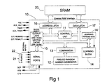
- the embodiment which will now be described with reference to Figures 1 and 2 is a module which provides 256 pRAMs, though some other number could be provided instead.
- the hardware for the module takes the form of a single VLSI chip 10 and a conventional static RAM 20, with appropriate connection between the two and provision for connection to other modules and/or to external inputs.
- the VLSI chip 10 comprises a control unit 11, a pseudo random number generator 12, a comparator 13, a learning block 14 with connections to receive, inter alia, learning parameters held in a store 14', a memory 15, and address and data latches 16 and 17 via which the chip 10 is connected to a static RAM 20.
- a(t) is the pRAM's binary output, and p, ⁇ are constants ⁇ [0,1].
- the delta function is included to make it clear that only the location which is actually addressed at time t is available to be modified, the contents of the other locations being unconnected with the behaviour that led to reward or punishment at time t.
- the store 14' hold the parameters ⁇ and ⁇ . These may be constant or they may vary with time to improve convergence.
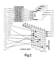
- the pRAMs of which three of the 256 are shown in Figure 2, are shown in that Figure as though each were a discrete physical entity, but, as will be apparent from the ensuing description, each is in fact a virtual pRAM.
- the storage locations for all the pRAMs are in the RAM 20, and the pseudo random number generator, comparator and learning block held on the VLSI serve successively as those components of each pRAM.
- each pRAM of the module in question (regarded as module 0) is stored in column 0 of what is referred to here as an output list which is part of the VLSI memory 15.
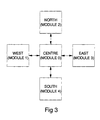
- Columns 1 to 4 hold the current values of the outputs of four other modules 1 to 4 to which the module in question is connected (see Figure 3).
- the description of this embodiment is on the basis that the module in question is connected to four other modules, but it must be understood that it might be connected to a greater or lesser number of modules, or to no other modules.
- the module has a single output port connected to all of its neighbours, and four serial input ports each connected to a respective neighbour. These ports are denoted by reference numeral 21.
- each pRAM is specified by associating each of the six address inputs of the pRAM with a respective one of the six connection pointers 0 to 5.
- the pointers can be held either in RAM 20 or on chip 10, preferably the former. These pointers indicate, inter alia, from which pRAM in which module (or from which external source) the input concerned is to be taken.
- the connection pointers denote the fact that the inputs to the pRAM 0 are taken from pRAM 5 in module 2, pRAM 3 in module 3, pRAM 7 in module 0, pRAM 4 in module 1, pRAM 3 in module 4, and an external input with address 5 respectively.
- the system does not use a pair of output lists, namely an "Old” output list consisting of five columns which contain the outputs of the module concerned, and those of the four modules to which it is connected, for the previous time step, and a "New" output list which holds the current pRAM outputs of the module concerned, as they are being generated.
- the "Old" output list is able to be omitted by ensuring that the pRAMs are processed in an appropriate order, beginning with those in the input layer of the network, continuing, in order, with those in any hidden layers, and finishing with those in the output layer.
- the problem which would otherwise arise where pairs of pRAMs are cross-coupled is dealt with using "dummy" pRAMs, a feature described in detail below. All modules are processed synchronously. Thus, the pRAMs 0 in all modules are processed at the same time, then all pRAMs 1, and so forth.
- Figure 1 shows that the on-chip memory 15 includes a vector cache consisting of 256 x 6 bits. This is to facilitate global learning, and the reason for it is as follows.
- the first pass calculates the new output state for each of the 256 pRAMS, from the input layer first through to the output pRAMs. After each layer is processed, the outputs are handed immediately to the following layer for processing within the first pass.
- the reward and penalty signals are determined by an external environment, and these signals are applied to each pRAM during the second pass.
- the previous state of the network, which caused the present output must be used in a reward/penalty reinforcement learning rule. This state could be re-created by fetching all connection pointers once more and forming the input vector for each neuron from the Output List as in the first pass.
- connection pointers illustrated in Figure 2.
- connection pointer P applies the value of the output of pRAM 1 in module 4, as stored in the Output List, as the penalty signal to the pRAM being processed
- connection pointer R applies the value of the output of pRAM 2 in module 4, as stored in the Output List, as the reward signal to the pRAM being processed.
- the output of other pRAMs could represent a form of competitive learning. If global learning is desired, the connection pointers point to the pins where the global reward and penalty signals are applied, and connection pointers for this purpose are included in a list given hereinafter.
- the above process is executed on each of the modules synchronously and respectively.
- Step (6) above refers to a form of reinforcement training known as global reward/penalty learning, in which the contents of at least one of the storage locations in the neuron (in this case a pRAM) are altered on the basis of signals from the environment signifying success or failure of the network as a whole (the reward and penalty signals, r and p).
- Suitable algorithms for carrying out such reinforcement training are described in the International Patent Applications mentioned above and in a paper entitled "Reinforcement training strategies for probabilistic RAMS" by D. Gorse and J.G. Taylor in: Proceedings of Euronet '90, Moscow, September 1990, pp 98-100.
- connection pointers used in the architecture of Figures 1 to 3 each consist of twelve bits. Bits 0 to 7 specify which of the pRAMs 0 to 255 is being accessed. Bits 8 to 11 specify the following data sources: Bit 8 9 10 11 Data Source 0 0 0 0 0 Same chip 1 0 0 0 0 North chip 0 1 0 0 East chip 1 1 0 0 South chip 0 0 1 0 West chip 1 0 1 0 External inputs 0 1 1 0 Vdd for permanent logic '1' 1 1 1 0 Ground for permanent logic '0' 0 0 0 1 Global reward pin 1 0 0 1 Global penalty pin
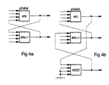
- pRAM 255 (in this example) which stores the state of pRAM N at time t-1.
- pRAM N+1 is therefore connected to pRAM 255 instead of pRAM N in order to receive the state of pRAM N at time t-1.
- pRAM 255 acts as a 'dummy' pRAM which stores the output state of one of the pRAMs and thus allows all the conditions concerning the order of processing to be met.
- the 'dummy' pRAM is one of the 256 pRAMs from the module which has its memory contents set either 11111111B or 00000000B.
- the 11111111B memory location is accessed when an input vector 1 is received and the 00000000B location is accessed whenever an input vector of O is received. In this way the pRAM always responds with a 1 or 0 respectively.
- This pRAM acts as a single delay element and is assigned a high pRAM number such that it is processed last ( Figure 4). A separate 'dummy' pRAM is needed for each cross-coupled connection in the network.
- HALT is an input which halts the chip at the end of a pass. Since the chip might be in the middle of a pass when HALT is asserted, ACK_HALT is used to signal when the chip has completed the pass and is now halted.
- an external device e.g. a computer
- TRAIN is an input which, when asserted, sets the chip into the training mode. Since the chip might be in the middle of a pass when TRAIN is asserted, ACK_TRAIN is used to signal when the chip has completed the pass and is now in the training mode.
- SOP is a serial output which outputs the new pRAM states and may be connected to the ports of other pRAM modules.
- RTS and CTS are Ready To Send and Clear To Send respectively. These handshaking signals synchronise the transfer of pRAM data between modules. All pRAM modules should operate synchronously, but one pRAM module might skip a clock cycle, for example, since there are separate clock dividers in each module. This would allow modules to get out of phase with each other.
- Each time a new pRAM output is produced in a multi-module system each module asserts RTS. All RTS outputs are connected together (wired-OR) and are connected to the CTS input of every module. All modules wait until the last RTS is asserted before continuing processing. In this way, the modules keep in step with each other.
Landscapes
- Engineering & Computer Science (AREA)
- Physics & Mathematics (AREA)
- Health & Medical Sciences (AREA)
- Life Sciences & Earth Sciences (AREA)
- Biomedical Technology (AREA)
- Biophysics (AREA)
- Theoretical Computer Science (AREA)
- Evolutionary Computation (AREA)
- General Engineering & Computer Science (AREA)
- Data Mining & Analysis (AREA)
- Artificial Intelligence (AREA)
- General Health & Medical Sciences (AREA)
- Molecular Biology (AREA)
- Computing Systems (AREA)
- Computational Linguistics (AREA)
- General Physics & Mathematics (AREA)
- Mathematical Physics (AREA)
- Software Systems (AREA)
- Neurology (AREA)
- Memory System Of A Hierarchy Structure (AREA)
- Complex Calculations (AREA)
Abstract
Claims (9)
- Unité de réseau neuronal ayant une pluralité de neurones, laquelle unité comprend une mémoire (20) fournissant une pluralité d'emplacements de stockage pour chacun des neurones, et dans un circuit intégré (10), des moyens (11, 12, 13, 15) pour définir un algorithme pour le fonctionnement des neurones, des moyens (14, 14') pour définir un algorithme d'apprentissage par lequel les neurones peuvent subir un processus d'apprentissage utilisant des signaux de récompense et de pénalité, et des moyens de commande (11, 16, 17) pour provoquer le traitement des neurones en séquence pour produire une sortie sur la base de données stockées dans lesdits emplacements de stockage et ledit algorithme, l'unité de réseau neuronal comprenant en outre une matrice de pointeurs de connexion définissant quelles sorties ou entrées externes de neurones sont connectées à quelles entrées de neurones, et caractérisée en ce que ledit réseau de pointeurs de connexion définit également quel signal de récompense et/ou de pénalité est appliqué à chacun des neurones, et caractérisé par un cache de vecteur pour stocker les adresses générées lors d'un passage de l'unité, pour utilisation dans un deuxième passage d'apprentissage, chaque dite adresse étant constituée des bits appliqués aux entrées de l'unité.
- Unité selon la revendication 1, dans laquelle la matrice de pointeurs de connexion est contenue dans ladite mémoire.
- Unité selon la revendication 1, dans laquelle la matrice de pointeurs de connexion est contenue dans ledit circuit intégré.
- Unité selon l'une quelconque des revendications précédentes, dans laquelle les moyens définissant l'algorithme de neurones comprennent un générateur de nombres aléatoires (12) et un comparateur (13) pour comparer le contenu des emplacements de stockage a des nombres aléatoires produits par ledit générateur de nombres aléatoires, le comparateur ayant une sortie à laquelle apparaît un signal ayant une première ou une deuxième valeur, selon le résultat de la comparaison, les sorties du comparateur constituant lesdites sorties de neurones.
- Unité selon l'une quelconque des revendications précédentes, dans laquelle au moins l'un des neurones a mains de la totalité de ses entrées connectées pour recevoir des données provenant d'autres sorties de neurones ou d'entrées externes, et chaque entrée qui n'est pas ainsi connectée est associée au moyen d'un pointeur de connexion à une entrée fournissant un '0' logique permanent ou un '1' logique permanent.
- Unité selon l'une quelconque des revendications précédentes, dans laquelle le cache de vecteur est sur le circuit intégré.
- Unité selon l'une quelconque des revendications précédentes, comportant des connexions à couplage croisé entre au moins certains des neurones et dans laquelle, pour chaque connexion à couplage croisé, est prévu un neurone fictif qui reçoit en tant qu'entrée une sortie provenant du neurone destiné à être traité en premier, et a sa sortie connectée à une entrée du neurone destiné à être traité en deuxième, auquel il fournit une entrée identique à l'entrée qu'il a lui-même reçue.
- Unité selon l'une quelconque des revendications précédentes, pourvue au moins d'un point d'accès d'extension (21) susceptible de permettre la connexion de l'unité au moins à une autre telle unité.
- Matrice d'une pluralité d'unités, chacune selon la revendication 8, les unités étant incerconnectées par l'intermédiaire desdits points d'accès d'extension.
Applications Claiming Priority (3)
| Application Number | Priority Date | Filing Date | Title |
|---|---|---|---|
| GB929226192A GB9226192D0 (en) | 1992-12-16 | 1992-12-16 | Neural network architecture |
| GB9226192 | 1992-12-16 | ||
| PCT/GB1993/002540 WO1994014134A1 (fr) | 1992-12-16 | 1993-12-13 | Architecture de reseau neuronal |
Publications (2)
| Publication Number | Publication Date |
|---|---|
| EP0674792A1 EP0674792A1 (fr) | 1995-10-04 |
| EP0674792B1 true EP0674792B1 (fr) | 1997-04-23 |
Family
ID=10726688
Family Applications (1)
| Application Number | Title | Priority Date | Filing Date |
|---|---|---|---|
| EP94902070A Expired - Lifetime EP0674792B1 (fr) | 1992-12-16 | 1993-12-13 | Architecture de reseau neuronal |
Country Status (5)
| Country | Link |
|---|---|
| EP (1) | EP0674792B1 (fr) |
| AU (1) | AU5657694A (fr) |
| DE (1) | DE69310210T2 (fr) |
| GB (1) | GB9226192D0 (fr) |
| WO (1) | WO1994014134A1 (fr) |
Families Citing this family (3)
| Publication number | Priority date | Publication date | Assignee | Title |
|---|---|---|---|---|
| MY138544A (en) * | 2003-06-26 | 2009-06-30 | Neuramatix Sdn Bhd | Neural networks with learning and expression capability |
| US8606732B2 (en) | 2010-08-04 | 2013-12-10 | Qualcomm Incorporated | Methods and systems for reward-modulated spike-timing-dependent-plasticity |
| US8892487B2 (en) | 2010-12-30 | 2014-11-18 | International Business Machines Corporation | Electronic synapses for reinforcement learning |
-
1992
- 1992-12-16 GB GB929226192A patent/GB9226192D0/en active Pending
-
1993
- 1993-12-13 AU AU56576/94A patent/AU5657694A/en not_active Abandoned
- 1993-12-13 EP EP94902070A patent/EP0674792B1/fr not_active Expired - Lifetime
- 1993-12-13 WO PCT/GB1993/002540 patent/WO1994014134A1/fr not_active Ceased
- 1993-12-13 DE DE69310210T patent/DE69310210T2/de not_active Expired - Fee Related
Also Published As
| Publication number | Publication date |
|---|---|
| EP0674792A1 (fr) | 1995-10-04 |
| GB9226192D0 (en) | 1993-02-10 |
| DE69310210D1 (de) | 1997-05-28 |
| DE69310210T2 (de) | 1997-11-27 |
| WO1994014134A1 (fr) | 1994-06-23 |
| AU5657694A (en) | 1994-07-04 |
Similar Documents
| Publication | Publication Date | Title |
|---|---|---|
| US5564115A (en) | Neural network architecture with connection pointers | |
| JP2517410B2 (ja) | 学習機能付集積回路装置 | |
| US5479574A (en) | Method and apparatus for adaptive classification | |
| JP3251421B2 (ja) | 半導体集積回路 | |
| US5075889A (en) | Arrangement of data cells and neural network system utilizing such an arrangement | |
| US5170463A (en) | Neuro-computer | |
| Burr | Digital neural network implementations | |
| JPH05505268A (ja) | デイジーチェーン制御付ニューラルネットワーク | |
| JPH03209561A (ja) | 連立一次方程式の解を求める計算装置及び方法 | |
| JPH04232562A (ja) | コンピユータ装置 | |
| Yasunaga et al. | A self-learning digital neural network using wafer-scale LSI | |
| US5408677A (en) | Vector parallel computer | |
| EP0674792B1 (fr) | Architecture de reseau neuronal | |
| Viredaz | MANTRA I: An SIMD processor array for neural computation | |
| Serrano-Gotarrdeona et al. | An ART1 microchip and its use in multi-ART1 systems | |
| WO1991019259A1 (fr) | Architecture distributive et numerique de maximalisation, et procede | |
| Bak et al. | Memory capacity of artificial neural networks with high order node connections | |
| JPH05197705A (ja) | ニューラルネットワークの学習システム | |
| Ruckert | An associative memory with neural architecture and its VLSI implementation | |
| JPH08504527A (ja) | ニューラルネットワーク・アーキテクチャ | |
| Rückert | VLSI Design of an associative memory based on distributed storage of information | |
| JPH04233062A (ja) | ベクトルの処理方法およびその回路 | |
| JP3246764B2 (ja) | ニューロチップ | |
| Hendrich | A scalable architecture for binary couplings attractor neural networks | |
| Hahanov et al. | Automaton MQT-model for virtual computer design |
Legal Events
| Date | Code | Title | Description |
|---|---|---|---|
| PUAI | Public reference made under article 153(3) epc to a published international application that has entered the european phase |
Free format text: ORIGINAL CODE: 0009012 |
|
| 17P | Request for examination filed |
Effective date: 19950531 |
|
| AK | Designated contracting states |
Kind code of ref document: A1 Designated state(s): DE FR GB IT |
|
| GRAG | Despatch of communication of intention to grant |
Free format text: ORIGINAL CODE: EPIDOS AGRA |
|
| 17Q | First examination report despatched |
Effective date: 19960412 |
|
| GRAH | Despatch of communication of intention to grant a patent |
Free format text: ORIGINAL CODE: EPIDOS IGRA |
|
| GRAH | Despatch of communication of intention to grant a patent |
Free format text: ORIGINAL CODE: EPIDOS IGRA |
|
| GRAA | (expected) grant |
Free format text: ORIGINAL CODE: 0009210 |
|
| AK | Designated contracting states |
Kind code of ref document: B1 Designated state(s): DE FR GB IT |
|
| PG25 | Lapsed in a contracting state [announced via postgrant information from national office to epo] |
Ref country code: IT Free format text: LAPSE BECAUSE OF FAILURE TO SUBMIT A TRANSLATION OF THE DESCRIPTION OR TO PAY THE FEE WITHIN THE PRE;WARNING: LAPSES OF ITALIAN PATENTS WITH EFFECTIVE DATE BEFORE 2007 MAY HAVE OCCURRED AT ANY TIME BEFORE 2007. THE CORRECT EFFECTIVE DATE MAY BE DIFFERENT FROM THE ONE RECORDED.SCRIBED TIME-LIMIT Effective date: 19970423 |
|
| REF | Corresponds to: |
Ref document number: 69310210 Country of ref document: DE Date of ref document: 19970528 |
|
| ET | Fr: translation filed | ||
| PLBE | No opposition filed within time limit |
Free format text: ORIGINAL CODE: 0009261 |
|
| STAA | Information on the status of an ep patent application or granted ep patent |
Free format text: STATUS: NO OPPOSITION FILED WITHIN TIME LIMIT |
|
| 26N | No opposition filed | ||
| PGFP | Annual fee paid to national office [announced via postgrant information from national office to epo] |
Ref country code: FR Payment date: 19981209 Year of fee payment: 6 |
|
| PGFP | Annual fee paid to national office [announced via postgrant information from national office to epo] |
Ref country code: GB Payment date: 19981218 Year of fee payment: 6 |
|
| PGFP | Annual fee paid to national office [announced via postgrant information from national office to epo] |
Ref country code: DE Payment date: 19981221 Year of fee payment: 6 |
|
| PG25 | Lapsed in a contracting state [announced via postgrant information from national office to epo] |
Ref country code: GB Free format text: LAPSE BECAUSE OF NON-PAYMENT OF DUE FEES Effective date: 19991213 |
|
| GBPC | Gb: european patent ceased through non-payment of renewal fee |
Effective date: 19991213 |
|
| PG25 | Lapsed in a contracting state [announced via postgrant information from national office to epo] |
Ref country code: FR Free format text: LAPSE BECAUSE OF NON-PAYMENT OF DUE FEES Effective date: 20000831 |
|
| PG25 | Lapsed in a contracting state [announced via postgrant information from national office to epo] |
Ref country code: DE Free format text: LAPSE BECAUSE OF NON-PAYMENT OF DUE FEES Effective date: 20001003 |
|
| REG | Reference to a national code |
Ref country code: FR Ref legal event code: ST |