EP0673072B1 - Semiconductor device comprising a lateral bipolar transistor - Google Patents
Semiconductor device comprising a lateral bipolar transistor Download PDFInfo
- Publication number
- EP0673072B1 EP0673072B1 EP95301625A EP95301625A EP0673072B1 EP 0673072 B1 EP0673072 B1 EP 0673072B1 EP 95301625 A EP95301625 A EP 95301625A EP 95301625 A EP95301625 A EP 95301625A EP 0673072 B1 EP0673072 B1 EP 0673072B1
- Authority
- EP
- European Patent Office
- Prior art keywords
- region
- semiconductor
- type
- semiconductor region
- transistor
- Prior art date
- Legal status (The legal status is an assumption and is not a legal conclusion. Google has not performed a legal analysis and makes no representation as to the accuracy of the status listed.)
- Expired - Lifetime
Links
Images



Classifications
-
- H—ELECTRICITY
- H10—SEMICONDUCTOR DEVICES; ELECTRIC SOLID-STATE DEVICES NOT OTHERWISE PROVIDED FOR
- H10D—INORGANIC ELECTRIC SEMICONDUCTOR DEVICES
- H10D10/00—Bipolar junction transistors [BJT]
- H10D10/311—Thin-film BJTs
-
- H—ELECTRICITY
- H10—SEMICONDUCTOR DEVICES; ELECTRIC SOLID-STATE DEVICES NOT OTHERWISE PROVIDED FOR
- H10D—INORGANIC ELECTRIC SEMICONDUCTOR DEVICES
- H10D10/00—Bipolar junction transistors [BJT]
- H10D10/60—Lateral BJTs
-
- H—ELECTRICITY
- H10—SEMICONDUCTOR DEVICES; ELECTRIC SOLID-STATE DEVICES NOT OTHERWISE PROVIDED FOR
- H10D—INORGANIC ELECTRIC SEMICONDUCTOR DEVICES
- H10D12/00—Bipolar devices controlled by the field effect, e.g. insulated-gate bipolar transistors [IGBT]
- H10D12/411—Insulated-gate bipolar transistors [IGBT]
-
- H—ELECTRICITY
- H10—SEMICONDUCTOR DEVICES; ELECTRIC SOLID-STATE DEVICES NOT OTHERWISE PROVIDED FOR
- H10D—INORGANIC ELECTRIC SEMICONDUCTOR DEVICES
- H10D18/00—Thyristors
- H10D18/251—Lateral thyristors
Definitions
- n-type base region is formed on one main surface side of n-type body region, this n-type base region has a higher impurity concentration than that of the body region, and p-type emitter region is formed in this n-type base region.
- p-n-p transistor is disclosed in the above stated JP-A-59 127 865.
- the second p-collector region becomes the collector, besides during a high voltage application time the depletion layer spreads out in the second p-collector region and further the first collector becomes the collector.
- An auxiliary electrode 44 is provided on the semiconductor body 10.
- An external resistor R1 is connected between the auxiliary electrode 44 and the base electrode 41. Namely, the semiconductor body 10 and the n-type base region 11 are connected through the resistor R1.
- the sheet resistance of the p-type collector region becomes small, the breakdown voltage lowers.
- the resistor R1 is connected between the auxiliary electrode 44 and the base electrode 41, the lowering degree of the breakdown voltage is small.
- An electrode is provided respectively on each of the above exposed portions. Namely, as shown in Fig. 4, a collector electrode C (a first electrode) 43 is provided on the p+ region 22 of the p-type collector region 23, a base electrode B (a second electrode) 41 is provided on the n+ region 12 of the n-type base region 11, and an emitter electrode E (a third electrode) 42 is provided on the exposed portion of the p-type emitter region 42.
- a projecting portion is provided at an end portion (a left end portion in Fig. 4) and this projecting portion extends over the p-type collector region 23 and the n-type semiconductor body 10.
- a thickness of the monocrystalline island region 3 is 40 ⁇ m
- the maximum impurity concentration and a diffusion depth of the n-type buried layer 19 are 5 x 10 18 /cm 3 and 11 ⁇ m
- a resistivity of the n-type semiconductor body 10 is 20 ⁇ cm.
- the cutoff frequency can be made high.
- the breakdown voltage can be improved.
- the current flowing into the p-type collector region 23 from the p-type emitter region 23 flows toward for a lateral direction along to the main surface and also flows toward a direction of the p-type collector region 23 positioned just directly under the p-type emitter region 21, namely toward for a vertical direction.
- each semiconductor region will not limited to the above stated numerical values but may select other suitable values.
- the depth of the p+ region 22 is 0.5 ⁇ m but the deeper depth than the above may be selected, even in this case then the element characteristic does not receive the affects.
- the cutoff frequency can be improved without the lowering in the breakdown voltage.
- an interval (n-base width) formed between the p-type emitter region 21 and the p-type collector region 23 can be made narrow. Accordingly, the current amplification factor and the cutoff frequency can be improved.
- the diffusion depth of the n+ buried layer 19 is reduced at 8 ⁇ m from 11 ⁇ m. Further, the thickness of the monocrystalline island region 3 can be reduced and the element dimension can be made small.
- the sheet resistance of the region for providing this semiconductor region 24 can be made small.
- the sheet resistance is made as 8 k ⁇ / ⁇ , which is the same degree of the sheet resistance of the p-type collector region 23 arranged on the main surface.
Landscapes
- Bipolar Transistors (AREA)
- Insulated Gate Type Field-Effect Transistor (AREA)
Description
- The present invention relates to a semiconductor device comprising a lateral bipolar transistor.
- As for a transistor for use in a power IC or in LSI and transistor for a signal, a high breakdown voltage and a high speed bipolar type semiconductor device is required. However, in a single transistor, it is difficult to satisfy these above stated characteristics at the same time.
- For the above stated reasons, in a case in which one characteristic is improved, another characteristic is sacrificed some degree. For example, so as to obtain the high speed transistor, a base width is made narrow and thereby the breakdown voltage is sacrificed.
- As stated in the above, because the high breakdown voltage and high speed bipolar type transistor is not able to realize, in particular in the bipolar linear type IC, the following problems will occur.
- In the bipolar linear type IC, so as to increase the degrees of freedom for designing a circuit and further so as to simplify a circuit structure, both n-p-n transistor and p-n-p transistor are used in together. In this time, so as to lessen a number of manufacturing processes, the n-p-n transistor is formed with a vertical type structure and the p-n-p transistor is formed with a lateral type structure.
- In the lateral type p-n-p transistor, in an "off" condition, a depletion layer spreads out to a semiconductor base substance region having a low impurity concentration. In this time, it is necessary to prevent a punch-through phenomenon in which the depletion layer reaches to an emitter junction and then the current flows.
- For this reasons, an interval (base width) between an emitter region and a collector region is formed wider than the width of the depletion layer in the voltage to be checked by the transistor. As a result, an operation frequency of the lateral type p-n-p transistor lowers remarkably comparing with that of the vertical structure n-p-n transistor.
- As an element structure for solving the problems in the above stated lateral type transistor, p-n-p transistor disclosed disclosed in JP-A-59 127 865 is known.
- In this p-n-p transistor, n-type base region is formed on one main surface side of n-type body region, this n-type base region has a higher impurity concentration than that of the body region, and p-type emitter region is formed in this n-type base region.
- In the same body region, a first p-type collector region is formed separately from the n-type base region. Further, a second p-type collector region is formed so as to contact to the first p-type collector region and further so as to surround around the n-type base region. The second p-type collector region has a lower impurity concentration than those of the first p-type collector region and the n-type base region.
- In this p-n-p transistor having the above stated structure, the depletion layer mainly spreads out toward the second collector region having the low impurity concentration. Accordingly, even if the width of the n-type base region is formed narrow, the punch-through phenomenon does not occur. As a result, both the breakdown voltage and the operation frequency in the p-n-p transistor can be improved at the same time.
- However, using the above stated lateral type p-n-p transistor, there is a limit in the obtainment for the high frequency. Namely, the cutoff frequency fT is 70 MHz at the breakdown voltage of 100 V, and in the breakdown voltage of 350 V the cutoff frequency fT is 25 MHz, these cutoff frequency fT values are 1/5 - 1/10 in comparison with the value in the n-p-n transistor having the same breakdown voltage.
- For the above stated reasons, the performances in the bipolar linear type IC are limited by the characteristics of the lateral type p-n-p transistor.
- Besides, generally, in a power IC, LSI and a transistor for signal, a high breakdown voltage, a high current amplification factor and a high speed transistor is needed. However, it is difficult to realize the above stated characteristics at the same time.
- In a prior art so as to realize the high current amplification factor, there are methods in which a method for thinning a base region at the expense of the breakdown voltage and a method for forming a Darlington transistor structure at the expense of speed.
- For example, in a bipolar linear type IC, there are serious affects when a high breakdown voltage, a high current amplification factor and a high speed bipolar type transistor is not realized at the same time. Because, in the lateral structure p-n-p transistor, a collector junction breakdown voltage is attained by the spread of a depletion layer in a base region (semiconductor body region) having a low concentration.
- However, so as to prevent a punch-through phenomenon an interval (base width) between an emitter and a collector is designed wider than the width of the depletion layer in a design breakdown voltage in a collector junction. As a result, the current amplification factor is lowered remarkably comparing with the vertical structure transistor.
- So as to solve the above stated problems in the lateral type transistor various kinds of the element structures have proposed. For one example, p-n-p transistor is disclosed in the above stated JP-A-59 127 865. With the above stated transistor structure, during a low voltage application time the second p-collector region becomes the collector, besides during a high voltage application time the depletion layer spreads out in the second p-collector region and further the first collector becomes the collector.
- As a result the current amplification factor and the cutoff frequency and the breakdown voltage of the transistor can be improved at the same time.
- However, in the above transistor structure, there pays no attention to the base resistance, during the use of the linear IC since the base resistance is large, a problem occurs in which the noise voltage is made large. So as to solve this problem, a transistor structure shown in JP-A-3 132 037 (& DE-A-4 032 816) is well known.
- In the above transistor structure, a part of the first collector region for surrounding around the n-base region in the p-n-p transistor disclosed in the above stated JP-A-59 127 865 is released.
- In the released part the n-base region having a high impurity concentration is connected to a second base region having high impurity concentration for use in an external portion base electrode of the first collector region.
- According to this transistor structure, the base resistance can be made small, as a result the p-n-p transistor having the low noise voltage can be formed.
- An example with respect to the p-n-p transistor having the high breakdown voltage and the high speed linear type IC as an exemplified and representative problem will be explained.
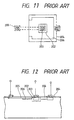
- So as to realize the high breakdown voltage and the higher speed linear type integrated circuit (IC), a plan view and a cross-sectional view showing the lateral type p-n-p transistor disclosed in the above stated JP-A-3 132 047 are shown in Fig. 11 and Fig. 12.
- So as to improve the cutoff frequency, when a width of the n-
base region 202 for forming an effective operation region and formed between p-emitter region 203 and p-collector region 206 is remarkably narrow, the contribution degree affected to the base resistance and the collector resistance becomes large and thereby the base resistance and the collector resistance are needed to reduce. - Besides, in a case for obtaining the high breakdown voltage, the length of the
second collector region 206 for working as the electric field relaxation region and formed between the n-base region 202 and the first p-collector region 204 becomes longer, as a result, the collector resistance increases. Further, the distance of the second n-base region 205 drawn from the n-base region 202 becomes long, as a result the base resistance increases. - So as to reduce the resistances, the base impurity concentration of the drawn-out
portion 205 is made higher than that of the first n-base region 202, so that during the reversal bypass application time of the transistor, the electron concentration at the contact portion of the impurity material at the second p-collector region 206 and the second n-base region 205 is remarkable, thereby the lowering in the breakdown voltage is invited. - So as to prevent the lowering in the breakdown voltage, the lowering in the impurity concentration of the
second collector region 206 is needed, as a result the collector resistance increases and the lowering in the cutoff frequency occurs. - Besides, in this transistor, so as to increase the current capacity, the
emitter region 203 is made long toward an opposite side of the second n-base region 205, since the relation between the first n-base region 202 and the p-emitter region 203 is determined according to the current amplification factor. - As a result, during the high current operation time, the voltage between the emitter and the base becomes low going to toward an opposite side of the direction of the second n-
base region 205, because of the non-uniformity in the voltage between the emitter and the base, the lowering in the current amplification factor, the cutoff frequency and the noise voltage in the high current region occur. - GB-A-1428742 discloses a vertical bipolar transistor in which a p-type substrate is covered by an n+ collector layer including an aperture. A p base layer, formed on the n+ collector layer, extends through the aperture to contact the substrate, whereby a resistor connected to the base layer is provided.
- An object of the present invention is to provide a semiconductor device comprising a lateral bipolar transistor, wherein a frequency characteristics can be improved without the sacrifice of the breakdown voltage.
- Another object of the present invention is to provide a semiconductor device comprising a lateral bipolar transistor, wherein a superior noise characteristic, a high breakdown voltage characteristic and a high frequency characteristic can be obtained without sacrificing the breakdown voltage.
- The present invention provides a semiconductor device comprising a lateral bipolar transistor, said bipolar transistor comprising:
- a first conductivity type semiconductor body having a main surface;
- a second conductivity type first semiconductor region in said semiconductor body and adjoining said main surface of said semiconductor body, the first semiconductor region forming a collector of the transistor;
- a first conductivity type second semiconductor region provided on said first semiconductor region and having an impurity concentration higher than that of said first semiconductor region, the second semiconductor region forming a base of the transistor;
- a second conductivity type third semiconductor region provided on said second semiconductor region the third semiconductor region forming a emitter of the transistor;
- a first electrode ohmically contacting said first semiconductor region;
- a second electrode ohmically contacting said second semiconductor region; and
- a third electrode ohmically contacting said third semiconductor region; wherein a resistance region electrically connects said semiconductor body and said second semiconductor region.
-
- According to the present invention, in the lateral bipolar transistor, the operation can be made speedy without the lowering in the breakdown voltage. As a result, since the lateral bipolar transistor having the same frequency characteristics as those of the vertical bipolar transistor can be realized, the performance of the bipolar linear type IC using both semiconductor devices together can be improved.
- In the drawings:
- Fig. 1 is a cross-sectional view for explaining a principle structure of a semiconductor device according to the present invention;
- Fig. 2 is a graph showing a relationship between a sheet resistance of p-type collector region and a breakdown voltage between a collector electrode and an emitter electrode;
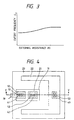
- Fig. 3 is a graph showing a relationship between an external resistance between an auxiliary electrode and a base electrode and a cutoff frequency;
- Fig. 4 is a plan view showing a first embodiment of a semiconductor device according to the present invention;
- Fig. 5 is a cross-sectional view showing the first embodiment of the semiconductor device according to the present invention and taken along to a line V-V of Fig. 4;
- Fig. 6 is a cross-sectional view showing a second embodiment of a semiconductor device according to the present invention;
- Fig. 7 is a cross-sectional view showing a third embodiment of a semiconductor device according to the present invention;
- Fig. 8 is a cross-sectional view showing a fourth embodiment of a semiconductor device according to the present invention;
- Fig. 9 is a cross-sectional view showing a fifth embodiment of a semiconductor device according to the present invention;
- Fig. 10 is a cross-sectional view showing a sixth embodiment of a semiconductor device according to the present invention; and
- Figs. 11 and 12 are plan and sectional views of the lateral type p-n-p transistor of JP-A-3 132 037 and have already been discussed.
-
- Hereinafter, various embodiments of semiconductor devices will be explained referring to the drawings.
- According to the above stated features of the present invention, the reasons in which in the lateral type semiconductor device wherein without the sacrifice of the breakdown voltage the frequency characteristics can be improved will be explained as followings.
- First of all, a principle structure of a semiconductor device according to the present invention. Fig. 1 is a cross-sectional view for explaining a principle structure of a semiconductor device according to the present invention. In the lateral bipolar transistor shown in Fig. 1, p-
type collector region 23 is provided on at a main surface of n-type semiconductor body (n-) 10. - n-
type base region 11 forming a second semiconductor region is provided on this p-type collector region 23. The impurity concentration of the n-type base region 11 is higher than the impurity concentration of the p-type collector region 23. p-type emitter region 21 and a region (n+) 12 having a higher impurity concentration than that of the n-type base region 11 are provided in the n-type base region 11. - Further, an insulating
film 31 comprised of a silicon oxide and a buriedlayer 19 are provided on the semiconductor device. A collector electrode C (a first electrode) 43 is provided on ap+ region 22 of the p-type collector region 23, a base electrode B (a second electrode) 41 is provided on then+ region 12 of the n-type base region 11, and an emitter electrode E (a third electrode) 42 is provided on the exposed portion of the p-type emitter region 42, respectively. - An
auxiliary electrode 44 is provided on thesemiconductor body 10. An external resistor R1 is connected between theauxiliary electrode 44 and thebase electrode 41. Namely, thesemiconductor body 10 and the n-type base region 11 are connected through the resistor R1. - Fig. 2 is a graph showing an examination study by the inventors of the present invention with respect to a relationship between a sheet resistance of the p-
type collector region 23 and a breakdown voltage between a collector electrode and an emitter electrode in the semiconductor device shown in Fig. 1. - This Fig. 2 is the examination results in one case in which the external resistor R1 is connected between the
auxiliary electrode 44 and thebase electrode 41, shown by a curve line X, and another case in which the interval between theauxiliary electrode 44 and thebase electrode 41 is not connected through a resistor, shown by a curve line Y. - In either cases, the sheet resistance of the p-type collector region becomes small, the breakdown voltage lowers. However, in the case in which the resistor R1 is connected between the
auxiliary electrode 44 and thebase electrode 41, the lowering degree of the breakdown voltage is small. - Fig. 3 is a view showing an examination study by the inventors of the present invention with respect to a relationship between the external resistor R1 and the cutoff frequency fT.
- When the value of the resistor R1 is made large, the cutoff frequency fT becomes higher. This is that in Fig. 1 a junction capacity C between p-
type collector region 23 and the n-type semiconductor body 10 is connected to the n-type base region 11 through a resistance part R of thesemiconductor body 10 and the resistor R1 between theauxiliary electrode 44 and thebase electrode 41. - Namely, within the signal current for supplying the
base electrode 41, a part being the charging current for the junction capacity C is restrained due to the resistor R1, as a result a net base current to be contributed for the carrier injection from the p-type emitter region 21 increases. - As stated in above, in the lateral type semiconductor device according to the present invention, the
semiconductor body 10 and the semiconductor region forming the base region are connected by the resistor R1, and by increasing the resistance value, the cutoff frequency fT can be improved. Further, by the provision of the resistor R1 the lowering of the breakdown voltage can be prevented. - Hereinafter, one embodiment of a semiconductor device according to the present invention will be explained in detail.
- Fig. 4 and Fig. 5 show a first embodiment of a semiconductor device according to the present invention. This first embodiment shows a lateral type p-n-p transistor which is formed on a dielectric body isolating substrate.
- First of all, a cross-sectional structure of the first embodiment of the lateral type p-n-p transistor according to the present invention will be explained referring to Fig. 5.
- In a dielectric body isolating substrate 1, a
monocrystalline island region 3 is provided on a supportingmember 61 comprised of polycrystalline silicon, and the supportingmember 61 and theisland shape region 3 are separated by an insulatingfilm 31 comprised of a silicon oxide. - The monocrystalline
island shape region 3 has n-type buriedlayer 19 and n-type semiconductor body 10, thissemiconductor body 10 is adjacently provided with the buriedlayer 19. - p-type collector region (a first semiconductor region) 23 is provided on a side of a
main surface 2 of themonocrystalline island region 3 of the dielectric body isolating substrate 1. n-type base region (a second semiconductor region) 11 is provided in this p-type collector region 23. - A junction depth of this n-
type base region 11 is shallower than that of the p-type collector region 23. An impurity concentration of the n-type base region 11 is larger than that of the p-type collector 23. The n-type base region 11 is connected to the n-type semiconductor body 10 at an end portion (a left end portion in Fig. 5) in which the n-type base region 11 contacts to themain surface 2. - Further, p-type emitter region (a third semiconductor region) 21 is provided in the n-
type base region 11. A junction depth of this p-type emitter region 21 is shallower than that of the n-type base region 11 and an impurity concentration of the p-type emitter region 21 is larger than that of the n-type base region 11. - The p-
type collector region 23 is positioned just directly under the p-type emitter region 21. In this first embodiment of the present invention, the p-type collector region 23 is positioned just directly under the p-type emitter region 21 all over, however the p-type collector region 23 may be positioned just directly partially under the p-type emitter region 21. - Most of the
main surface 2 is covered by the insulatingfilm 31 comprised of the silicon oxide. However, by partially removing the insulatingfilm 31 the surfaces of the p-type collector region 23, the n-type base region 11 and the p-type emitter region 21 are exposed. - Herein,
p+ region 22 is provided at the exposed portion of the p-type collector region 23, and an impurity concentration of thep+ region 22 is larger than that of the p-type collector region 23. Further,n+ region 12 is provided at the exposed portion of the n-type base region 11, and an impurity concentration of then+ region 12 is larger than that of the n-type base region 11. - An electrode is provided respectively on each of the above exposed portions. Namely, as shown in Fig. 4, a collector electrode C (a first electrode) 43 is provided on the
p+ region 22 of the p-type collector region 23, a base electrode B (a second electrode) 41 is provided on then+ region 12 of the n-type base region 11, and an emitter electrode E (a third electrode) 42 is provided on the exposed portion of the p-type emitter region 42. - All of the p-
type collector region 23, the n-type base region 11, the p-type emitter region 21, thep+ region 22 and then+ region 12 are formed according to a common thermal diffusion method. - Next, a planar structure of the semiconductor device of this first embodiment according to the present invention will be explained referring to Fig. 4.
- The p-
type collector region 23 has a square shape pattern or a rectangular shape pattern. This n-type collector 23 region surrounds around all most of the n-type base region 11, namely as shown in Fig. 4, the n-type collector region 23 surrounds around a region on which the p-type emitter region 21 and then+ region 12 are provided. - A projecting portion is provided at an end portion (a left end portion in Fig. 4) and this projecting portion extends over the p-
type collector region 23 and the n-type semiconductor body 10. - This projecting portion forms a resistance region (14) for connecting the n-
type base region 11 and the n-type semiconductor body 10. A resistance value is adjusted according to the dimension of the projecting portion. Further, the projecting portion may have a different junction depth and a different impurity concentration with the n-type base region 11, when the projecting portion is formed with a conductivity type semiconductor region same as the n-type base region 11. - In the above case, it is possible to adjust the resistance value according to both the dimension and the impurity concentration of the projecting portion, thereby a range of the resistance value being able to set can be widely determined.
- Further, the
p+ region 22 in the p-type collector region 23 opposes to a surrounding portion of the n-type base region 11, except for the above stated projecting portion. - An exemplified example of the dimension and the impurity concentration of the respective part according to the semiconductor device of this first embodiment according to the present invention will be explained as following.
- A thickness of the
monocrystalline island region 3 is 40 µm, the maximum impurity concentration and a diffusion depth of the n-type buriedlayer 19 are 5 x 10¹⁸/cm3 and 11 µm, and a resistivity of the n-type semiconductor body 10 is 20 Ω·cm. - A sheet resistance and a diffusion depth of the p-
type collector region 23 provided on themain surface 2 side of themonocrystalline island region 3 are 8 kΩ/□ and 9 µm. - A surface concentration and a diffusion depth of the n-
type base region 11 are 1 x 10¹⁷/cm3 and 2 µm, and a surface concentration and a diffusion depth of the p-type emitter region 21 are 5 x 10¹⁹/cm3 and 0.5 µm. - A surface concentration and a diffusion depth of the
p+ region 22 are 5 x 10¹⁹/cm3 and 0.5 µm, and a surface concentration and a diffusion depth of then+ region 12 are 1 x 10²⁰/cm3 and 0.4 µm. Further, a sheet resistance value of the p-type collector region 23 positioned just directly under the n-type base region 11 is 15 kΩ/□. - The dimension except for the projection portion of the n-
type base region 11 is 45 µm x 15 µm, and each of a dimension of the p-type emitter region 21 and thep+ region 12 provided on the n-type base region 11 is 15 µm x 9 µm, and an interval between the p-type emitter region 21 and thep+ region 12 is 5 µm. - A vertical direction of the n-
type base region 11 is the same vertical directions of the p-type emitter region 21 and then+ region 12. An interval between the p-type emitter region 21 and then+ region 12 and the p-type collector region 23 is 3 µm in a portion except for the projecting portion of the p-type collector region 23. - The projecting portion of the n-
type base region 11 projects 5 µm toward the n-type semiconductor body 10 from the end portion of the p-type collector region 23. At thep+ region 22, a width of the region parallel to the vertical direction of the n-type base region 11 is 6 µm, and a width of the region vertical to the vertical direction of thebase region 11 is 15 µm. - In the vertical direction of the n-
type base region 11, an interval between the n-type base region 11 and thep+ region 22 is 20 µm. A distance between an end portion of thep+ region 22 and an end portion of the p-type collector region 23 is 15 µm at a portion except for the projecting portion of the n-type base region 11. - Further, each dimension of opening
portions film 31 is 3 µm x 9 µm, and a dimension of anopening portion 53 is 9 µm x 3 µm. - According to this first embodiment, the projection portion continuously provided on the n-
type base region 11 forms the resistance region (14). The junction capacity of the p-type collector region 23 and the n-type semiconductor body 10 connected to the n-type base region 11 through the resistance part of the resistance region (14) comprised of the projecting portion and thesemiconductor body 10. - As a result, according to the above resistance region (14) and the resistance part the base current being given to the
base electrode 41 is restrained to make the charging current of the junction capacity. - Thereby, even when the frequency of the base current becomes high, since the net base current for contributing the carrier injection from the p-type emitter region does not reduce, the cutoff frequency can be made high.
- Further, since an interval between the n-
type base region 11 and thesemiconductor body 10 does not present the open condition, the breakdown voltage can be improved. - According to the results by the inventor's study of the present invention, for example, in the case of the lateral type p-n-p transistor having the above stated dimensions and the impurity concentrations, the breakdown voltage between the collector and the emitter is 250 V and the cutoff frequency is 280 MHz at the collector current of 0.7 mA. This value of the cutoff frequency is extremely higher than that of the conventional lateral bipolar transistor.
- Further, this first embodiment has following effects. As shown in Fig. 4, the p-
type collector region 23 is positioned just directly under the p-type emitter region 21. - As a result, the current flowing into the p-
type collector region 23 from the p-type emitter region 23 flows toward for a lateral direction along to the main surface and also flows toward a direction of the p-type collector region 23 positioned just directly under the p-type emitter region 21, namely toward for a vertical direction. - Consequently, since the current concentration in the transistor becomes small, the current amplification factor becomes large and the "on" voltage becomes low.
- In the semiconductor device of this first embodiment according to the present invention, so as to secure the breakdown voltage between the p-
type collector region 23 and the n-type substrate which corresponds to the potential difference between the collector electrode and thesemiconductor body 10 in the use condition of the p-n-p transistor, a distance between the end portion of thep+ region 22 and the end portion of the p-type collector region 23 is secured with 15 µm. - However, this portion will be formed through another electric field relaxation method, for example, a field plate formation etc. and the similar effects can be obtained, and then the reliability can be further improved.
- Further, the dimension and the impurity concentration of each semiconductor region will not limited to the above stated numerical values but may select other suitable values. For example, the depth of the
p+ region 22 is 0.5 µm but the deeper depth than the above may be selected, even in this case then the element characteristic does not receive the affects. - Fig. 6 shows a cross-sectional structure of p-n-p transistor of a second embodiment according to the present invention. In this second embodiment, the n-
type base region 11 is provided in the interior portion of the p-type collector region 23. Namely, in this second embodiment of the present invention, an end portion of the n-type base region 11 does not project toward for the n-type semiconductor body 10, as shown in the former first embodiment of the present invention. - Just directly under the n-
type base region 11, a portion is formed, however on this portion the p-type collector region 23 is not provided. This portion forms a resistance region (14') and at this portion the n-type base region 11 and the n-type semiconductor body 10 are connected to each other. - As a result, in this second embodiment according to the present invention, similar to the former first embodiment of the present invention, the cutoff frequency can be improved without the lowering in the breakdown voltage.
- Further, in this second embodiment of the present invention, a resistance value of the resistance region can be adjusted according to the shape and the dimension of the portion on which the p-
type collector region 23 is not provided. - Accordingly, only changing a host mask pattern during the formation of the p-type collector region, the resistance value of the resistance region can be easily and widely adjusted.
- Fig. 7 shows a cross-sectional structure of p-n-p transistor of a third embodiment according to the present invention generally similar to that of the first embodiment. In this third embodiment of the present invention, however at least the region of the p-
type emitter region 21 opposing to the p-type collector region 23 is formed with the same diffusion window of the n-type base region 11 in the first embodiment of the present invention. - As a result, in this third embodiment of the present invention, at the region in which the p-
type emitter region 21 is opposed to the p-type collector region 23, both the p-type emitter region 21 and the n-type base region 11 have a substantially concentric circular shape each other. - With the p-n-p transistor having the above stated construction, an interval (n-base width) formed between the p-
type emitter region 21 and the p-type collector region 23 can be made narrow. Accordingly, the current amplification factor and the cutoff frequency can be improved. - Further, in this third embodiment of the present invention, the diffusion depth and the sheet resistance value of the p-
type collector region 23 are 6 µm and 8 kΩ /□. The dimensions and the impurity concentration of the other portions have the same numeric values shown in the first embodiment of the present invention. For this reasons, the p-type collector region 23 positioned just directly under the p-type emitter region 21 has the large value of 50 kΩ/□. - In the above stated p-n-p transistor, since the p-
type collector region 23 positioned just directly under the p-type emitter region 21 has the high resistance, it contributes a little for the operation. For this reasons, in the interior portion of the transistor, the current mainly flows to the lateral direction parallel to the main surface of thesemiconductor body 10. - In particular, with the above stated lateral type p-n-p transistor, the structure of this third embodiment have following effects. Namely, since an interval (n-base width) formed between the p-
type emitter region 21 and the p-type collector region 23 can be made narrow, even in a case since the current mainly flows toward for the lateral direction parallel to the main surface, thereby the current amplification factor and the cutoff frequency can be improved. - According to the results by the inventors's study of the present invention, the characteristics of this transistor are following. In other words, the breakdown voltage between the collector and the emitter is 250 V and the cutoff frequency is 230 MHz at the collector current of 0.5 mA. The above cutoff frequency is remarkably higher than that of the conventional semiconductor device.
- Further, each of the diffusion temperature and the time for forming the p-
type collector region 23 is 1200°C and 1000 minutes, respectively, in a case of the first embodiment according to the present invention. - However, in this third embodiment according to the present, each of the diffusion temperature and the time for forming the p-
type collector region 23 is 1200°C and 400 minutes, thereby the time for forming the p-type collector region 23 is made shorter as 400 minutes. - As a result, the diffusion depth of the n+ buried
layer 19 is reduced at 8 µm from 11 µm. Further, the thickness of themonocrystalline island region 3 can be reduced and the element dimension can be made small. - Fig. 8 shows a cross-sectional structure of p-n-p transistor of a fourth embodiment according to the present invention.
- In this fourth embodiment according to the present invention, p-
type semiconductor region 24 having the higher impurity concentration than that of the p-type collector region 23 is provided on the p-type collector region 23 positioned just directly under the p-type emitter region 21 in the third embodiment of the present invention. - By the provision of the p-
type semiconductor region 24, the sheet resistance of the region for providing thissemiconductor region 24 can be made small. For example, the sheet resistance is made as 8 kΩ/□, which is the same degree of the sheet resistance of the p-type collector region 23 arranged on the main surface. - Accordingly, since the collector resistance is made small, the cutoff frequency can be improved.
- According to the results by the inventors's study of the present invention, the characteristics of this transistor of the fourth embodiment according to the present invention are following. In other words, the breakdown voltage between the collector and the emitter is 250 V and the cutoff frequency is 310 MHz at the collector current of 0.5 mA. The above cutoff frequency is can be improved comparing with the first embodiment of the present invention.
- Fig. 9 shows a cross-sectional structure of p-n-p transistor of a fifth embodiment according to the present invention.
- In this fifth embodiment according to the present invention, the n-
type base region 11 is provided in the interior portion of the p-type collector region 23. Namely, an end portion of the n-type base region 11 does not project toward for the n-type semiconductor body 10 as shown in the former embodiment of the present invention. - n-
type semiconductor region 15 is provided on the n-typesemiconductor base substance 10 and theauxiliary electrode 44 for taking out the potential of the n-typesemiconductor base substance 10 is provided and ohmically contacts to thesemiconductor region 15. The resistance region is aresistor 62 comprised of the polycrystalline silicon formed on the insulatingfilm 31 and connected between theauxiliary electrode 44 and thebase electrode 41. - As a result, independently of the dimensions and the impurity concentrations of the respective semiconductor regions, the resistance value for connecting the n-
type base region 11 and the n-typesemiconductor base substance 10 can be determined. - Namely, regardless of the relation of the transistor structure, the high resistance value can be set. As a result, the cutoff frequency can be improved as shown in Fig. 3.
- Further, in this fifth embodiment according to the present invention, in particularly, in a case that the n-
type semiconductor body 10 has the low resistance value, the remarkable effects can be obtained. - Namely, since the resistance value can be heightened regardless of the relation of the resistivity of the n-
type semiconductor body 10, even in the semiconductor device having the low resistivity the lowering in the cutoff frequency can be prevented. - Fig. 10 shows a cross-sectional structure of p-n-p transistor of a sixth embodiment according to the present invention.
- In this sixth embodiment according to the present invention, the n-
type base region 11 is provided in the interior portion of the p-type collector region 23. The n-type semiconductor body 10 and the n-type base region 11 are connected through the n-type semiconductor region 15 forming the resistance region. - According to the above sixth embodiment of the present invention, the resistance value of the n-
type semiconductor region 15 can be adjusted according to the impurity concentration or to the dimensions of the n-type semiconductor region 15. - As a result, even when the resistivity of the n-
type semiconductor body 10 is small and further the impurity concentration of the n-type base region 11 is high, the resistance for connecting the n-typesemiconductor base substance 10 and the n-type base region 11 can be made large. Accordingly, the cutoff frequency can be improved.
Claims (9)
- A semiconductor device comprising a lateral bipolar transistor, said bipolar transistor comprising:wherein a resistance region (14,14',15,62) electrically connects said semiconductor body (10) and said second semiconductor region (11).a first conductivity type semiconductor body (10) having a main surface;a second conductivity type first semiconductor region (23) in said semiconductor body (10) and adjoining said main surface of said semiconductor body (10), the first semiconductor region (23) forming a collector of the transistor;a first conductivity type second semiconductor region (11) provided on said first semiconductor region (23) and having an impurity concentration higher than that of said first semiconductor region (23), the second semiconductor region (11) forming a base of the transistor;a second conductivity type third semiconductor region (21) provided on said second semiconductor region (11), the third semiconductor region (21) forming a emitter of the transistor;a first electrode (43, 47) ohmically contacting said first semiconductor region (23);a second electrode (41) ohmically contacting said second semiconductor region(11); anda third electrode (42) ohmically contacting said third semiconductor region (21);
- A semiconductor device according to claim 1, wherein said first semiconductor region (23) extends directly under said third semiconductor region (21), and said resistance region (14,14',15) is in an interior portion of said semiconductor body (10).
- A semiconductor device according to claim 2, wherein said second semiconductor region (11) is electrically connected by said resistance region (14, 14', 15) to said semiconductor body (10) at an end portion of said second semiconductor region (11) which adjoins said main surface of said semiconductor body (10).
- A semiconductor device according to claim 2, wherein said second semiconductor region (11) has a projecting portion of the first conductivity type which projects toward said semiconductor body (10), and said projecting portion forms said resistance region (14).
- A semiconductor device according to claim 2, wherein said resistance region (14') is formed by a portion of said semiconductor body (10) located directly under said second semiconductor region (11), said first semiconductor region (23) being not provided at said portion.
- A semiconductor device according to any one of claims 1 to 5, wherein at a region where said first semiconductor region (23) and said third semiconductor region (21) face each other along said main surface, said second semiconductor region (11) and said third semiconductor region (21) have a substantially concentrically circular shape.
- A semiconductor device according to any one of claims 1 to 6, wherein a semiconductor region (24) of the second conductivity type and having an impurity concentration higher than that of said first semiconductor region (23) is disposed directly under said third semiconductor region (21) in said first semiconductor region (23).
- A semiconductor device according to claim 1, wherein said resistance region (62) is a polycrystalline semiconductor region disposed on an insulator (31) located on said main surface of said semiconductor body (10).
- A semiconductor device according to any one of claims 1 to 8, further comprising a semiconductor substrate (61) having a plurality of island regions which are arranged side by side and electrically insulated from said semiconductor substrate, said semiconductor body (10) forming one of said islands.
Applications Claiming Priority (6)
| Application Number | Priority Date | Filing Date | Title |
|---|---|---|---|
| JP4826294 | 1994-03-18 | ||
| JP48262/94 | 1994-03-18 | ||
| JP6048262A JPH07263455A (en) | 1994-03-18 | 1994-03-18 | Semiconductor device |
| JP6073780A JPH07263456A (en) | 1994-03-22 | 1994-03-22 | Semiconductor device |
| JP73780/94 | 1994-03-22 | ||
| JP7378094 | 1994-03-22 |
Publications (3)
| Publication Number | Publication Date |
|---|---|
| EP0673072A2 EP0673072A2 (en) | 1995-09-20 |
| EP0673072A3 EP0673072A3 (en) | 1995-11-08 |
| EP0673072B1 true EP0673072B1 (en) | 2003-05-28 |
Family
ID=26388498
Family Applications (1)
| Application Number | Title | Priority Date | Filing Date |
|---|---|---|---|
| EP95301625A Expired - Lifetime EP0673072B1 (en) | 1994-03-18 | 1995-03-13 | Semiconductor device comprising a lateral bipolar transistor |
Country Status (4)
| Country | Link |
|---|---|
| US (1) | US5608236A (en) |
| EP (1) | EP0673072B1 (en) |
| KR (1) | KR950034825A (en) |
| DE (1) | DE69530881D1 (en) |
Families Citing this family (5)
| Publication number | Priority date | Publication date | Assignee | Title |
|---|---|---|---|---|
| US5945726A (en) | 1996-12-16 | 1999-08-31 | Micron Technology, Inc. | Lateral bipolar transistor |
| DE19844531B4 (en) * | 1998-09-29 | 2017-12-14 | Prema Semiconductor Gmbh | Process for the production of transistors |
| US6563193B1 (en) * | 1999-09-28 | 2003-05-13 | Kabushiki Kaisha Toshiba | Semiconductor device |
| JP5052091B2 (en) * | 2006-10-20 | 2012-10-17 | 三菱電機株式会社 | Semiconductor device |
| CN100529773C (en) * | 2006-11-10 | 2009-08-19 | 群康科技(深圳)有限公司 | Integrate circuit system pressing impedance detection method |
Family Cites Families (10)
| Publication number | Priority date | Publication date | Assignee | Title |
|---|---|---|---|---|
| US3631311A (en) * | 1968-03-26 | 1971-12-28 | Telefunken Patent | Semiconductor circuit arrangement with integrated base leakage resistance |
| GB1428742A (en) * | 1973-06-02 | 1976-03-17 | Ferranti Ltd | Semiconductor devices |
| US4231056A (en) * | 1978-10-20 | 1980-10-28 | Harris Corporation | Moat resistor ram cell |
| JPS5948951A (en) * | 1982-09-14 | 1984-03-21 | Toshiba Corp | Semiconductor protective device |
| JPS59127865A (en) * | 1983-01-12 | 1984-07-23 | Hitachi Ltd | Semiconductor device |
| JPH0654795B2 (en) * | 1986-04-07 | 1994-07-20 | 三菱電機株式会社 | Semiconductor integrated circuit device and manufacturing method thereof |
| JPH01112764A (en) * | 1987-10-27 | 1989-05-01 | Nec Corp | Semiconductor device |
| IT1230895B (en) * | 1989-06-22 | 1991-11-08 | Sgs Thomson Microelectronics | INTEGRABLE POWER TRANSISTOR WITH OPTIMIZATION OF DIRECT SECONDARY BREAKING PHENOMENA. |
| JP2507632B2 (en) * | 1989-10-18 | 1996-06-12 | 株式会社日立製作所 | Semiconductor device |
| US5293051A (en) * | 1992-02-14 | 1994-03-08 | Sharp Kabushiki Kaisha | Photoswitching device including a MOSFET for detecting zero voltage crossing |
-
1995
- 1995-03-13 DE DE69530881T patent/DE69530881D1/en not_active Expired - Lifetime
- 1995-03-13 EP EP95301625A patent/EP0673072B1/en not_active Expired - Lifetime
- 1995-03-15 US US08/404,465 patent/US5608236A/en not_active Expired - Fee Related
- 1995-03-17 KR KR1019950005533A patent/KR950034825A/en not_active Ceased
Also Published As
| Publication number | Publication date |
|---|---|
| US5608236A (en) | 1997-03-04 |
| DE69530881D1 (en) | 2003-07-03 |
| KR950034825A (en) | 1995-12-28 |
| EP0673072A3 (en) | 1995-11-08 |
| EP0673072A2 (en) | 1995-09-20 |
Similar Documents
| Publication | Publication Date | Title |
|---|---|---|
| KR100199273B1 (en) | Insulated gate semiconductor device and manufacturing method thereof | |
| USRE33209E (en) | Monolithic semiconductor switching device | |
| US4546536A (en) | Fabrication methods for high performance lateral bipolar transistors | |
| KR100683100B1 (en) | Semiconductor integrated circuit device and manufacturing method thereof | |
| US4583106A (en) | Fabrication methods for high performance lateral bipolar transistors | |
| JP2968222B2 (en) | Semiconductor device and method for preparing silicon wafer | |
| EP0093304A1 (en) | Semiconductor IC and method of making the same | |
| JP2017195406A (en) | Trench gate insulated gate bipolar transistor and method of manufacturing the same | |
| JPH0758784B2 (en) | Lateral insulated gate bipolar transistor with improved latch-up prevention performance | |
| KR20060115756A (en) | High Energy Electrostatic Discharge Structure and Method | |
| EP0680090B1 (en) | Protection device against electrostatic discharges | |
| EP0036319B1 (en) | Semiconductor device | |
| US4051506A (en) | Complementary semiconductor device | |
| CN112768447A (en) | Reverse conducting insulated gate bipolar transistor and manufacturing method thereof | |
| JP3644697B2 (en) | Integrated structure current sensing resistor for power MOS devices | |
| US3786318A (en) | Semiconductor device having channel preventing structure | |
| US5323041A (en) | High-breakdown-voltage semiconductor element | |
| US4686557A (en) | Semiconductor element and method for producing the same | |
| US5608236A (en) | Semiconductor device | |
| US5624855A (en) | Process of producing insulated-gate bipolar transistor | |
| US4109273A (en) | Contact electrode for semiconductor component | |
| US4520382A (en) | Semiconductor integrated circuit with inversion preventing electrode | |
| US4864379A (en) | Bipolar transistor with field shields | |
| JP3311166B2 (en) | Insulated gate semiconductor device | |
| JP2949001B2 (en) | Gate insulated semiconductor device and method of manufacturing the same |
Legal Events
| Date | Code | Title | Description |
|---|---|---|---|
| PUAI | Public reference made under article 153(3) epc to a published international application that has entered the european phase |
Free format text: ORIGINAL CODE: 0009012 |
|
| PUAL | Search report despatched |
Free format text: ORIGINAL CODE: 0009013 |
|
| 17P | Request for examination filed |
Effective date: 19950403 |
|
| AK | Designated contracting states |
Kind code of ref document: A2 Designated state(s): DE FR GB SE |
|
| AK | Designated contracting states |
Kind code of ref document: A3 Designated state(s): DE FR GB SE |
|
| 17Q | First examination report despatched |
Effective date: 19961217 |
|
| GRAG | Despatch of communication of intention to grant |
Free format text: ORIGINAL CODE: EPIDOS AGRA |
|
| RIC1 | Information provided on ipc code assigned before grant |
Free format text: 7H 01L 29/735 A |
|
| RTI1 | Title (correction) |
Free format text: SEMICONDUCTOR DEVICE COMPRISING A LATERAL BIPOLAR TRANSISTOR |
|
| RIC1 | Information provided on ipc code assigned before grant |
Free format text: 7H 01L 29/735 A |
|
| RTI1 | Title (correction) |
Free format text: SEMICONDUCTOR DEVICE COMPRISING A LATERAL BIPOLAR TRANSISTOR |
|
| GRAG | Despatch of communication of intention to grant |
Free format text: ORIGINAL CODE: EPIDOS AGRA |
|
| GRAH | Despatch of communication of intention to grant a patent |
Free format text: ORIGINAL CODE: EPIDOS IGRA |
|
| GRAH | Despatch of communication of intention to grant a patent |
Free format text: ORIGINAL CODE: EPIDOS IGRA |
|
| GRAA | (expected) grant |
Free format text: ORIGINAL CODE: 0009210 |
|
| AK | Designated contracting states |
Designated state(s): DE FR GB SE |
|
| PG25 | Lapsed in a contracting state [announced via postgrant information from national office to epo] |
Ref country code: FR Free format text: LAPSE BECAUSE OF FAILURE TO SUBMIT A TRANSLATION OF THE DESCRIPTION OR TO PAY THE FEE WITHIN THE PRESCRIBED TIME-LIMIT Effective date: 20030528 |
|
| REG | Reference to a national code |
Ref country code: GB Ref legal event code: FG4D |
|
| REG | Reference to a national code |
Ref country code: SE Ref legal event code: TRGR |
|
| REF | Corresponds to: |
Ref document number: 69530881 Country of ref document: DE Date of ref document: 20030703 Kind code of ref document: P |
|
| PG25 | Lapsed in a contracting state [announced via postgrant information from national office to epo] |
Ref country code: DE Free format text: LAPSE BECAUSE OF FAILURE TO SUBMIT A TRANSLATION OF THE DESCRIPTION OR TO PAY THE FEE WITHIN THE PRESCRIBED TIME-LIMIT Effective date: 20030829 |
|
| PG25 | Lapsed in a contracting state [announced via postgrant information from national office to epo] |
Ref country code: GB Free format text: LAPSE BECAUSE OF NON-PAYMENT OF DUE FEES Effective date: 20040313 |
|
| PG25 | Lapsed in a contracting state [announced via postgrant information from national office to epo] |
Ref country code: SE Free format text: LAPSE BECAUSE OF NON-PAYMENT OF DUE FEES Effective date: 20040314 |
|
| PLBE | No opposition filed within time limit |
Free format text: ORIGINAL CODE: 0009261 |
|
| STAA | Information on the status of an ep patent application or granted ep patent |
Free format text: STATUS: NO OPPOSITION FILED WITHIN TIME LIMIT |
|
| 26N | No opposition filed |
Effective date: 20040302 |
|
| EN | Fr: translation not filed | ||
| EUG | Se: european patent has lapsed | ||
| GBPC | Gb: european patent ceased through non-payment of renewal fee |
Effective date: 20040313 |