EP0671807B1 - Schaltnetzteil mit Informationsübertragung von der Primärseite zur Sekundärseite - Google Patents
Schaltnetzteil mit Informationsübertragung von der Primärseite zur Sekundärseite Download PDFInfo
- Publication number
- EP0671807B1 EP0671807B1 EP95103177A EP95103177A EP0671807B1 EP 0671807 B1 EP0671807 B1 EP 0671807B1 EP 95103177 A EP95103177 A EP 95103177A EP 95103177 A EP95103177 A EP 95103177A EP 0671807 B1 EP0671807 B1 EP 0671807B1
- Authority
- EP
- European Patent Office
- Prior art keywords
- signal
- power supply
- voltage
- switched
- pulse
- Prior art date
- Legal status (The legal status is an assumption and is not a legal conclusion. Google has not performed a legal analysis and makes no representation as to the accuracy of the status listed.)
- Expired - Lifetime
Links
- 238000004804 winding Methods 0.000 claims description 13
- 239000003990 capacitor Substances 0.000 claims description 4
- 230000008878 coupling Effects 0.000 claims description 2
- 238000010168 coupling process Methods 0.000 claims description 2
- 238000005859 coupling reaction Methods 0.000 claims description 2
- 230000001105 regulatory effect Effects 0.000 claims description 2
- 230000001276 controlling effect Effects 0.000 claims 1
- 238000010586 diagram Methods 0.000 description 2
- 238000009499 grossing Methods 0.000 description 2
- 230000008054 signal transmission Effects 0.000 description 2
- 230000001419 dependent effect Effects 0.000 description 1
- 238000002955 isolation Methods 0.000 description 1
- 230000000630 rising effect Effects 0.000 description 1
Images


Classifications
-
- H—ELECTRICITY
- H03—ELECTRONIC CIRCUITRY
- H03J—TUNING RESONANT CIRCUITS; SELECTING RESONANT CIRCUITS
- H03J9/00—Remote-control of tuned circuits; Combined remote-control of tuning and other functions, e.g. brightness, amplification
-
- H—ELECTRICITY
- H02—GENERATION; CONVERSION OR DISTRIBUTION OF ELECTRIC POWER
- H02M—APPARATUS FOR CONVERSION BETWEEN AC AND AC, BETWEEN AC AND DC, OR BETWEEN DC AND DC, AND FOR USE WITH MAINS OR SIMILAR POWER SUPPLY SYSTEMS; CONVERSION OF DC OR AC INPUT POWER INTO SURGE OUTPUT POWER; CONTROL OR REGULATION THEREOF
- H02M3/00—Conversion of DC power input into DC power output
- H02M3/22—Conversion of DC power input into DC power output with intermediate conversion into AC
- H02M3/24—Conversion of DC power input into DC power output with intermediate conversion into AC by static converters
- H02M3/28—Conversion of DC power input into DC power output with intermediate conversion into AC by static converters using discharge tubes with control electrode or semiconductor devices with control electrode to produce the intermediate AC
- H02M3/325—Conversion of DC power input into DC power output with intermediate conversion into AC by static converters using discharge tubes with control electrode or semiconductor devices with control electrode to produce the intermediate AC using devices of a triode or a transistor type requiring continuous application of a control signal
- H02M3/335—Conversion of DC power input into DC power output with intermediate conversion into AC by static converters using discharge tubes with control electrode or semiconductor devices with control electrode to produce the intermediate AC using devices of a triode or a transistor type requiring continuous application of a control signal using semiconductor devices only
- H02M3/33507—Conversion of DC power input into DC power output with intermediate conversion into AC by static converters using discharge tubes with control electrode or semiconductor devices with control electrode to produce the intermediate AC using devices of a triode or a transistor type requiring continuous application of a control signal using semiconductor devices only with automatic control of the output voltage or current, e.g. flyback converters
- H02M3/33523—Conversion of DC power input into DC power output with intermediate conversion into AC by static converters using discharge tubes with control electrode or semiconductor devices with control electrode to produce the intermediate AC using devices of a triode or a transistor type requiring continuous application of a control signal using semiconductor devices only with automatic control of the output voltage or current, e.g. flyback converters with galvanic isolation between input and output of both the power stage and the feedback loop
Definitions
- the invention relates to a switching power supply according to the preamble of claim 1.
- Switching power supplies often require signals from Devices that are supplied with voltage on the primary side to transfer to facilities that are secondary be supplied with voltage. To the required electrical isolation in the signal path from the primary side to the secondary side To ensure it has been common to date, an optocoupler or an appropriately sized transformer to use. These components are only as discrete Embodiment known. The circuitry Realization is therefore complex and expensive.
- WO 93/11609 is a clocked circuit for transmitting a control signal for a high-voltage power transistor described via a transformer. By switching it in suitably switched DC voltages on the input side to the primary side of the Transformer voltage pulses occur on the secondary side of different shapes that are rectified.
- the object of the invention is a switching power supply with the possibility of signal transmission from the Primary to specify on the secondary side, that in comparison to previous solutions can be realized more easily.
- the invention is by a switching power supply according to the Features of claim 1 solved.
- the signal to be transmitted on the secondary side is the control signal, that determines the clock control of the switching power supply, modulated.
- the necessary modulation device on the primary side and secondary-side demodulation device can easily be implemented as integrated circuits will. Accordingly, there are no further complex ones discrete components necessary.
- the type of modulation should be such that the Voltage regulation of the switching power supply, which is usually by changing the on and off duration of the primary current is caused as little interference as possible becomes.
- a phase or Frequency modulation when a signal edge occurs transmitted signal.
- a phase modulation can consist, for example, that for one clock period the pulse-pause ratio of the control clock to one Value is changed that in normal operation of the fixed frequency Switching power supply does not occur.
- That to be transmitted Signal generated by a receiver for remote control signals After receiving the remote control signal, this becomes transferred to the secondary side and there in a control device fed.
- the control device e.g. a microcontroller, controls according to the received Command certain device functions.
- Particularly advantageous can be a switching power supply for remote control be used in connection with stand-by operation. With a remote control signal for setting the stand-by mode controlled, the switching power supply is switched off, so that the supplied electrical device as well as the microcontroller are without power.
- the receiver for the remote control however, the supply network becomes live fed. Since only the remote control receiver is in operation, the other functional units of the switching power supply are switched off, there is very little power loss consumed.
- An incoming remote control command for the The remote control receiver switches over to normal operation recognized and ensures that the switching power supply starts up. The device to be supplied and the microcontroller are then supplied with voltage. There can now be more Remote control commands are processed in the microcontroller.
- the usual clock frequency of the switching power supply is 50 kHz. For example, if after every 100 pulses of Control signal for the switching transistor a signal edge according to the invention from the primary to the secondary side is transmitted, a bit rate of 500 bits per second reached for signal transmission. Experience has shown that voltage regulation at such a low bit rate of the switching power supply hardly disturbed. For the transfer of Remote control signals whose bit rate is around 100 bits per second this data rate is sufficient. So it has to also no additional power reserve when dimensioning of the switching power supply are taken into account.
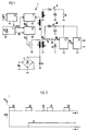
- a switched-mode power supply contains a transformer 1, to the primary winding 2 of which, by means of a switching transistor 3, a voltage rectified from the mains AC voltage U N by means of a rectifier 4, for example a bridge rectifier, and smoothed via a capacitor 5, is applied in a clocked manner.
- the on and off times of the switching transistor 3 are regulated such that the secondary voltage is as constant as possible regardless of the load to be supplied.
- a voltage proportional to the secondary voltage is tapped at a control winding 6 and fed to a control device 7.
- the control device 7 is essentially designed as an integrated circuit.
- the integrated control circuit TDA 4605 from Siemens can be used as the control device 7.
- the load 10 is supplied with voltage via a secondary winding 8 and a rectifier device 9 consisting of a diode and a smoothing capacitor.
- the switching power supply has a receiving device 11 for a remote control signal.
- the device 11 can contain, for example, an infrared receiver for remote control signals and a decoder.
- the remote control receiver 11 generates a signal IR which is to be transmitted to the secondary side in order to control device functions there.
- the signal IR is fed into a modulator 12, which modulates the switching signal U C supplied by the control device 7 in accordance with the signal IR to be transmitted.
- the transistor 3 is driven by the modulated control signal U G output by the modulator 12.
- the control pulses 30 generated by the control device 7 are set as a function of the control voltage supplied by the control winding 6 depending on the load.
- the modulator 12 inserts a short switch-on pulse 32 into the pulse train 30.
- the pulse duration of the pulse 32 is so small that the load-dependent voltage regulation is only slightly disturbed.
- a signal U S corresponding to the control signal U G for the switching transistor 3 in its pulse-pause ratios is tapped at a further secondary winding 14. The pulses of the signal U G are transmitted inverted to the secondary side.
- the voltage U S is freed from negative components and supplied to the demodulator 13.
- a coupling capacitor 20 is inserted between resistor 15 and diode 16, which ensures that the voltage swing is shifted even further into positive.
- the originally transmitted signal IR is demodulated in demodulator 13 and fed to a control device 17, for example a microcontroller. This controls, depending on the signal U O supplied to it, device functions of the switched-mode power supply and / or of the electronic device which is supplied with voltage and is represented as load 10. In the present case, the voltage supply to the demodulator 13 and the control device 17 is also ensured by the secondary winding 14 via a rectifier device 18.
- FIG. 1 An advantageous application of the switching power supply according to the invention results, as shown in FIG. 1, for the standby function of the switching power supply.
- the control device 7 and the modulator 12 are switched off by the corresponding command in the signal IR.
- the switching transistor 3 is then blocked, so that the secondary windings 8, 14 are de-energized.
- only remote control receiver 11 remains active, which is supplied with voltage from supply network with voltage U N via a power supply device 19.
- Conventional remote control receivers which, as already indicated above, essentially consist of an infrared preamplifier and corresponding decoders, consume relatively little power loss.
- Their power supply 19 can therefore be derived from the supply network in a low-loss manner without major component expenditure. This can be achieved for example by capacitive voltage division with subsequent rectification and smoothing or by rectification and subsequent ohmic voltage division. If necessary, the power supply device 19 is connected to the rectifier 4.
- FIG. 12 An exemplary embodiment of a modulator circuit 12 is shown in FIG. As essential elements, it contains a differentiator 40, which generates a positive pulse on both positive and negative edges of the remote control signal IR, an RS flip-flop 43, a D flip-flop 41 and a differentiator 42, which is positive directional pulse generated on a rising edge. This circuit ensures that a pulse 45 is generated on an edge of the signal IR, the length of which is substantially less than the pulse lengths of the signal U C that normally occur in switching operation.
- FIG. 4 shows a circuit implementation for the demodulator circuit 13.
- This contains a device 50 through which the pulse length of the signal U D is measured.
- the signal U D is clamped to ground by the diode 16 when the switching transistor 3 is closed. When switching transistor 3 is open, it is positive.
- the pulses to be evaluated are therefore directed negatively.
- the device 50 is shown in a gate implementation in which the pulse lengths of the signal U D are compared with a delay time set via an RC element 52, 53. If the pulse length does not exceed the value defined by the RC element, a pulse is generated in signal U F.
- the signal IR to be transmitted is reconstructed in a subsequent memory device, preferably a toggle flip-flop.
- the circuit 50 can also be implemented digitally by means of a pulse length counter (not shown).
- a pulse length counter contains, for example, a counter that is incremented as long as the signal U D has a negative pulse. If the pulse falls below a certain length, the output signal U F of the device 50 is set.
Landscapes
- Engineering & Computer Science (AREA)
- Power Engineering (AREA)
- Computer Hardware Design (AREA)
- Microelectronics & Electronic Packaging (AREA)
- Dc-Dc Converters (AREA)
- Cable Transmission Systems, Equalization Of Radio And Reduction Of Echo (AREA)
Description
- Figur 1
- ein erfindungsgemäßes Schaltnetzteil,
- Figur 2
- eine modulierte Impulsfolge,
- Figuren 3a und 3b
- eine schaltungstechnische Realisierung des Modulators sowie ein Impulsdiagramm und
- Figuren 4a und 4b
- eine schaltungstechnische Realisierung des Demodulators sowie ein Impulsdiagramm.
Claims (7)
- Schaltnetzteil enthaltendgekennzeichnet durcheinen Transformator (1) mit einer Primärwicklung (2) und mit einer Sekundärwicklung (14), die zur Versorgung einer Last (10) mit einer Ausgangsspannung dient, undMittel (7, 3, 4, 5) zum taktweisen Anlegen einer gleichgerichteten Spannung an die Primärwicklung (2) des Transformators (1), die von einem Steuersignal (UG) taktgesteuert werden, wobei die Ausgangsspannung über die Taktsteuerung der Mittel (7, 3, 4, 5) möglichst konstant geregelt wird,eine Modulationseinrichtung (12), durch die das Steuersignal (UG) in Abhängigkeit eines auf die Sekundärseite des Transformators (1) zu übertragenden Signals (IR) moduliert wird, undeine Demodulationseinrichtung (13), durch die das zu übertragende Signal (IR) aus einer an der Sekundärwicklung (14) des Transformators (1) anliegenden Spannung (US) demoduliert wird.
- Schaltnetzteil nach Anspruch 1,
gekennzeichnet durch
eine primärseitig mit Spannung versorgte Einrichtung (11) zum Empfang von Fernbediensignalen, durch die das zu übertragende Signal (IR) erzeugt wird, und eine sekundärseitig mit Spannung versorgte Steuerungseinrichtung (17) zur Steuerung von Funktionsabläufen in Abhängigkeit vom zu übertragenden Signal (IR), der das von der Demodulationseinrichtung (13) demodulierte Signal (UO) zugeführt wird. - Schaltnetzteil nach Anspruch 2,
dadurch gekennzeichnet,
daß die Einrichtung (11) zum Empfang von Fernbediensignalen aus einer Netzspannung (UN) versorgt wird. - Schaltnetzteil nach einem der Ansprüche 1 bis 3,
dadurch gekennzeichnet,
daß die Modulationseinrichtung (12) Mittel enthält, durch die die Länge eines Impulses des Steuersignals (UG) verkürzt wird, wenn das zu übertragende Signal (IR) eine Flanke aufweist, und daß die Demodulationseinrichtung (13) Mittel enthält, durch die eine Signalflanke erzeugt wird, wenn ein verkürzter Impuls erkannt wird. - Schaltnetzteil nach Anspruch 4,
dadurch gekennzeichnet,
daß die Demodulationseinrichtung (13) eine Einrichtung (50) enthält, durch die ein Impuls erzeugt wird, wenn das Eingangssignal (UD) der Demodulationseinrichtung (13) einen Impuls enthält, dessen Länge eine bestimmte Länge unterschreitet, und daß die Demodulationseinrichtung (13) ein von der Einrichtung (50) angesteuertes Speicherelement (51) enthält. - Schaltnetzteil nach einem der Ansprüche 1 bis 5,
dadurch gekennzeichnet,
daß ein Eingang der Demodulationseinrichtung (13) über einen Widerstand (15) mit einem Anschluß der Sekundärwicklung (14) verbunden ist, daß die Katode einer Diode (16) mit dem Eingang der Demodulationseinrichtung (13) verbunden ist und die Anode mit einem Anschluß für Sekundärmasse, und daß ein anderer Anschluß der Sekundärwicklung (14) mit dem Anschluß für Sekundärmasse verbunden ist. - Schaltnetzteil nach Anspruch 6,
dadurch gekennzeichnet,
daß zwischen den Widerstand (15) und die Diode (16) ein Koppelkondensator (20) geschaltet ist.
Applications Claiming Priority (2)
| Application Number | Priority Date | Filing Date | Title |
|---|---|---|---|
| DE4407529A DE4407529C1 (de) | 1994-03-07 | 1994-03-07 | Schaltnetzteil mit Informationsübertragung von der Primärseite zur Sekundärseite |
| DE4407529 | 1994-03-07 |
Publications (2)
| Publication Number | Publication Date |
|---|---|
| EP0671807A1 EP0671807A1 (de) | 1995-09-13 |
| EP0671807B1 true EP0671807B1 (de) | 1998-06-10 |
Family
ID=6512062
Family Applications (1)
| Application Number | Title | Priority Date | Filing Date |
|---|---|---|---|
| EP95103177A Expired - Lifetime EP0671807B1 (de) | 1994-03-07 | 1995-03-06 | Schaltnetzteil mit Informationsübertragung von der Primärseite zur Sekundärseite |
Country Status (3)
| Country | Link |
|---|---|
| EP (1) | EP0671807B1 (de) |
| DE (2) | DE4407529C1 (de) |
| ES (1) | ES2118461T3 (de) |
Families Citing this family (8)
| Publication number | Priority date | Publication date | Assignee | Title |
|---|---|---|---|---|
| WO1996025786A1 (en) * | 1995-02-16 | 1996-08-22 | Philips Electronics N.V. | Power-supply and communication |
| DE19520940C2 (de) * | 1995-06-02 | 1997-07-17 | Siemens Ag | Anordnung zur galvanisch getrennten Übertragung von Hilfsenergie (Gleichspannung) und Informationen zu einer elektronischen Einheit |
| DE19546359A1 (de) * | 1995-12-12 | 1997-06-19 | Siemens Ag | System mit zwei voneinander räumlich getrennten elektrischen Schaltungsanordnungen, und mit einer Leitung zwischen den Schaltungsanordnungen |
| DE19635611C2 (de) * | 1996-08-26 | 2000-06-21 | Rainer Kisthardt | Schaltungsanordnung (SAO) zur Senkung der Stromaufnahme, elektronischer und elektrischer Geräte im Stand- By - Betrieb |
| JP2001025251A (ja) * | 1999-07-05 | 2001-01-26 | Mitsumi Electric Co Ltd | 電源装置 |
| US6510066B2 (en) * | 2001-03-30 | 2003-01-21 | Demetri Giannopoulos | Switch mode power supply and method for transferring data across a power transformer |
| DE102009010260A1 (de) * | 2009-02-24 | 2010-09-02 | Osram Gesellschaft mit beschränkter Haftung | Schaltungsanordnung und Verfahren zum Betreiben einer Beleuchtungseinrichtung |
| DE102018124094A1 (de) * | 2018-09-28 | 2020-04-02 | Valeo Siemens Eautomotive Germany Gmbh | Stromrichter, Fahrzeug und Verfahren zum Betreiben eines Stromrichters |
Family Cites Families (4)
| Publication number | Priority date | Publication date | Assignee | Title |
|---|---|---|---|---|
| DE3501052A1 (de) * | 1985-01-15 | 1986-07-17 | Standard Elektrik Lorenz Ag, 7000 Stuttgart | Wandlerschaltung |
| US4996638A (en) * | 1990-02-15 | 1991-02-26 | Northern Telecom Limited | Method of feedback regulating a flyback power converter |
| FR2684500B1 (fr) * | 1991-12-02 | 1994-06-10 | Rahban Thierry | Generateur bipolaire a isolation galvanique de polarite commutable. |
| DE9309814U1 (de) * | 1993-07-01 | 1993-09-02 | Siemens AG, 80333 München | Standby-Schaltung für elektrische Verbraucher |
-
1994
- 1994-03-07 DE DE4407529A patent/DE4407529C1/de not_active Expired - Fee Related
-
1995
- 1995-03-06 DE DE59502452T patent/DE59502452D1/de not_active Expired - Lifetime
- 1995-03-06 ES ES95103177T patent/ES2118461T3/es not_active Expired - Lifetime
- 1995-03-06 EP EP95103177A patent/EP0671807B1/de not_active Expired - Lifetime
Also Published As
| Publication number | Publication date |
|---|---|
| EP0671807A1 (de) | 1995-09-13 |
| DE59502452D1 (de) | 1998-07-16 |
| ES2118461T3 (es) | 1998-09-16 |
| DE4407529C1 (de) | 1995-06-29 |
Similar Documents
| Publication | Publication Date | Title |
|---|---|---|
| EP0333275B1 (de) | Stromversorgungsanordnung | |
| DE69814073T2 (de) | Vollständig integrierte Einschaltregelschleife eines Hochspannungsleistungstransistors eines quasiresonanten Sperrwandlers | |
| DE3041134C2 (de) | Datenübertragungsanordnung zur Datenübertragung über eine Stromleitung | |
| DE69608184T2 (de) | Leistungsversorgung und übertragung | |
| WO1996038829A1 (de) | Anordnung zur galvanisch getrennten übertragung von hilfsenergie (gleichspannung) und informationen zu einer elektronischen einheit | |
| DE2345073A1 (de) | Netzgeraet | |
| DE3339193A1 (de) | Standby-stromversorgungsteil fuer einen fernsehempfaenger | |
| DE60223216T2 (de) | Kopplungseinrichtung für ein Übertragungssystem mit Trägerstrom niedriger Datenübertragungsrate | |
| DE68905507T2 (de) | Schaltungsanordnung zur ueberwachung der entmagnetisierung fuer einen sperrwandler mit primaerseitiger und secundaerseitiger regelung. | |
| DE4407529C1 (de) | Schaltnetzteil mit Informationsübertragung von der Primärseite zur Sekundärseite | |
| EP0689351A2 (de) | Schaltungsanordnung für den Wartebetrieb eines fernbedienbaren Gerätes | |
| DE2702277C2 (de) | ||
| EP0058754B1 (de) | Einrichtung zur Einspeisung von digitalen Signalen in ein Leitungssystem | |
| DE2411871B1 (de) | Schaltungsanordnung zur erdfreien Übertragung von Signalen über Trennstellen in Femmeldeanlagen | |
| EP0198263B1 (de) | Schaltungsanordnung zur erdfreien Übertragung digitaler Signale über Trennstellen | |
| EP0515421B1 (de) | Schaltnetzteil | |
| EP0941571B1 (de) | Schaltnetzteil mit regelung der ausgangsspannung | |
| EP0223171B1 (de) | Schaltnetzteil | |
| EP0509343A2 (de) | Verfahren zum Betreiben eines Schaltreglers sowie Anordnung | |
| DE2931436C2 (de) | Schaltungsanordnung zum Überwachen einer Eingangsspannung | |
| DE102020200672A1 (de) | Galvanisch getrenntes energietechnisches Koppeln von wenigstens zweipoligen Energieversorgungsleitungen | |
| EP0230930A2 (de) | Schaltnetzteil für ein fernbedienbares Gerät | |
| DE29515883U1 (de) | Schaltungsanordnung für ein Schaltnetzteil | |
| DE29614187U1 (de) | Busankoppler | |
| EP0309900B1 (de) | Schaltnetzteil |
Legal Events
| Date | Code | Title | Description |
|---|---|---|---|
| PUAI | Public reference made under article 153(3) epc to a published international application that has entered the european phase |
Free format text: ORIGINAL CODE: 0009012 |
|
| AK | Designated contracting states |
Kind code of ref document: A1 Designated state(s): DE ES FR GB IT |
|
| 17P | Request for examination filed |
Effective date: 19960205 |
|
| 17Q | First examination report despatched |
Effective date: 19961212 |
|
| GRAG | Despatch of communication of intention to grant |
Free format text: ORIGINAL CODE: EPIDOS AGRA |
|
| GRAG | Despatch of communication of intention to grant |
Free format text: ORIGINAL CODE: EPIDOS AGRA |
|
| GRAH | Despatch of communication of intention to grant a patent |
Free format text: ORIGINAL CODE: EPIDOS IGRA |
|
| GRAH | Despatch of communication of intention to grant a patent |
Free format text: ORIGINAL CODE: EPIDOS IGRA |
|
| GRAA | (expected) grant |
Free format text: ORIGINAL CODE: 0009210 |
|
| AK | Designated contracting states |
Kind code of ref document: B1 Designated state(s): DE ES FR GB IT |
|
| REF | Corresponds to: |
Ref document number: 59502452 Country of ref document: DE Date of ref document: 19980716 |
|
| ET | Fr: translation filed | ||
| GBT | Gb: translation of ep patent filed (gb section 77(6)(a)/1977) |
Effective date: 19980811 |
|
| ITF | It: translation for a ep patent filed | ||
| REG | Reference to a national code |
Ref country code: ES Ref legal event code: FG2A Ref document number: 2118461 Country of ref document: ES Kind code of ref document: T3 |
|
| PLBE | No opposition filed within time limit |
Free format text: ORIGINAL CODE: 0009261 |
|
| STAA | Information on the status of an ep patent application or granted ep patent |
Free format text: STATUS: NO OPPOSITION FILED WITHIN TIME LIMIT |
|
| 26N | No opposition filed | ||
| REG | Reference to a national code |
Ref country code: GB Ref legal event code: IF02 |
|
| PGFP | Annual fee paid to national office [announced via postgrant information from national office to epo] |
Ref country code: GB Payment date: 20020305 Year of fee payment: 8 |
|
| PGFP | Annual fee paid to national office [announced via postgrant information from national office to epo] |
Ref country code: ES Payment date: 20020321 Year of fee payment: 8 |
|
| PGFP | Annual fee paid to national office [announced via postgrant information from national office to epo] |
Ref country code: FR Payment date: 20020326 Year of fee payment: 8 |
|
| PG25 | Lapsed in a contracting state [announced via postgrant information from national office to epo] |
Ref country code: GB Free format text: LAPSE BECAUSE OF NON-PAYMENT OF DUE FEES Effective date: 20030306 |
|
| PG25 | Lapsed in a contracting state [announced via postgrant information from national office to epo] |
Ref country code: ES Free format text: LAPSE BECAUSE OF NON-PAYMENT OF DUE FEES Effective date: 20030307 |
|
| GBPC | Gb: european patent ceased through non-payment of renewal fee |
Effective date: 20030306 |
|
| PG25 | Lapsed in a contracting state [announced via postgrant information from national office to epo] |
Ref country code: FR Free format text: LAPSE BECAUSE OF NON-PAYMENT OF DUE FEES Effective date: 20031127 |
|
| REG | Reference to a national code |
Ref country code: FR Ref legal event code: ST |
|
| REG | Reference to a national code |
Ref country code: ES Ref legal event code: FD2A Effective date: 20030307 |
|
| PG25 | Lapsed in a contracting state [announced via postgrant information from national office to epo] |
Ref country code: IT Free format text: LAPSE BECAUSE OF NON-PAYMENT OF DUE FEES;WARNING: LAPSES OF ITALIAN PATENTS WITH EFFECTIVE DATE BEFORE 2007 MAY HAVE OCCURRED AT ANY TIME BEFORE 2007. THE CORRECT EFFECTIVE DATE MAY BE DIFFERENT FROM THE ONE RECORDED. Effective date: 20050306 |
|
| REG | Reference to a national code |
Ref country code: DE Ref legal event code: R081 Ref document number: 59502452 Country of ref document: DE Owner name: INFINEON TECHNOLOGIES AG, DE Free format text: FORMER OWNER: SIEMENS AKTIENGESELLSCHAFT, 80333 MUENCHEN, DE Effective date: 20111107 |
|
| PGFP | Annual fee paid to national office [announced via postgrant information from national office to epo] |
Ref country code: DE Payment date: 20140515 Year of fee payment: 20 |
|
| REG | Reference to a national code |
Ref country code: DE Ref legal event code: R071 Ref document number: 59502452 Country of ref document: DE |