EP0670656A2 - Bildaufnahmevorrichtung - Google Patents
Bildaufnahmevorrichtung Download PDFInfo
- Publication number
- EP0670656A2 EP0670656A2 EP95200467A EP95200467A EP0670656A2 EP 0670656 A2 EP0670656 A2 EP 0670656A2 EP 95200467 A EP95200467 A EP 95200467A EP 95200467 A EP95200467 A EP 95200467A EP 0670656 A2 EP0670656 A2 EP 0670656A2
- Authority
- EP
- European Patent Office
- Prior art keywords
- photosensitive
- rectifying
- elements
- row
- imaging
- Prior art date
- Legal status (The legal status is an assumption and is not a legal conclusion. Google has not performed a legal analysis and makes no representation as to the accuracy of the status listed.)
- Withdrawn
Links
Images


Classifications
-
- H—ELECTRICITY
- H10—SEMICONDUCTOR DEVICES; ELECTRIC SOLID-STATE DEVICES NOT OTHERWISE PROVIDED FOR
- H10F—INORGANIC SEMICONDUCTOR DEVICES SENSITIVE TO INFRARED RADIATION, LIGHT, ELECTROMAGNETIC RADIATION OF SHORTER WAVELENGTH OR CORPUSCULAR RADIATION
- H10F39/00—Integrated devices, or assemblies of multiple devices, comprising at least one element covered by group H10F30/00, e.g. radiation detectors comprising photodiode arrays
- H10F39/80—Constructional details of image sensors
- H10F39/803—Pixels having integrated switching, control, storage or amplification elements
-
- H—ELECTRICITY
- H04—ELECTRIC COMMUNICATION TECHNIQUE
- H04N—PICTORIAL COMMUNICATION, e.g. TELEVISION
- H04N25/00—Circuitry of solid-state image sensors [SSIS]; Control thereof
- H04N25/60—Noise processing, e.g. detecting, correcting, reducing or removing noise
- H04N25/62—Detection or reduction of noise due to excess charges produced by the exposure, e.g. smear, blooming, ghost image, crosstalk or leakage between pixels
- H04N25/621—Detection or reduction of noise due to excess charges produced by the exposure, e.g. smear, blooming, ghost image, crosstalk or leakage between pixels for the control of blooming
-
- H—ELECTRICITY
- H04—ELECTRIC COMMUNICATION TECHNIQUE
- H04N—PICTORIAL COMMUNICATION, e.g. TELEVISION
- H04N25/00—Circuitry of solid-state image sensors [SSIS]; Control thereof
- H04N25/70—SSIS architectures; Circuits associated therewith
- H04N25/76—Addressed sensors, e.g. MOS or CMOS sensors
-
- H—ELECTRICITY
- H10—SEMICONDUCTOR DEVICES; ELECTRIC SOLID-STATE DEVICES NOT OTHERWISE PROVIDED FOR
- H10F—INORGANIC SEMICONDUCTOR DEVICES SENSITIVE TO INFRARED RADIATION, LIGHT, ELECTROMAGNETIC RADIATION OF SHORTER WAVELENGTH OR CORPUSCULAR RADIATION
- H10F39/00—Integrated devices, or assemblies of multiple devices, comprising at least one element covered by group H10F30/00, e.g. radiation detectors comprising photodiode arrays
- H10F39/80—Constructional details of image sensors
- H10F39/802—Geometry or disposition of elements in pixels, e.g. address-lines or gate electrodes
- H10F39/8023—Disposition of the elements in pixels, e.g. smaller elements in the centre of the imager compared to larger elements at the periphery
Definitions
- This invention relates to an imaging device comprising an array of imaging elements each comprising a photosensitive element for sensing light incident on the imaging element and for storing charge representing the incident light and a rectifying element, the imaging elements being arranged in rows and columns with each photosensitive element and the associated rectifying element being coupled in series between an associated first conductor and an associated second conductor for allowing charge stored at a selected imaging element to be read out by applying voltages to the second conductors to forward bias the rectifying element of the selected imaging element to cause a current representing the charge stored at the photosensitive element of the selected imaging element to flow through the associated first conductor.
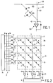
- Figure 1 of the accompanying drawings shows an example of an imaging element or pixel 101 of known imaging device 100.
- the image sensor 100 will comprise a two-dimensional matrix of rows N and column M of pixels with associated row 102 and column 103 conductors.
- N and column M the image sensor 100 will comprise a two-dimensional matrix of rows N and column M of pixels with associated row 102 and column 103 conductors.
- only one pixel is illustrated in Figure 1.
- the pixel 101 comprises a photosensitive diode PD and a switching diode SD coupled in series between the associated row conductor 102 and associated column conductor 103.
- the switching diode SD and photosensitive diode PD are arranged with the cathodes coupled together.
- a capacitor C is shown coupled across the photosensitive diode PD.
- the capacitor C may be the parasitic capacitance of the photosensitive diode PD or may be an additional capacitor added to increase the dynamic range of the image sensor 100.
- Each column conductor 103 is coupled to a suitable charge sensitive amplifier 104 having a capacitive coupling between its negative input and its output.
- vertical cross-talk may result from unwanted currents from unselected pixels flowing down the column or first conductor.
- the integrated output from the charge sensitive amplifier 8 for the selected pixel may include contributions from all of the other pixels in that column.
- the main source of the unwanted column currents is "dynamic leakage" from the unselected pixels in that column.
- the capacitance C of the photosensitive diode PD is being discharged by the photo-generation of charge carriers within the photosensitive diode PD, which in turn means that the voltage across the switching diode SD is changing.
- the changing voltage V x at the midpoint J between the two diodes causes a current: to flow through the capacitance C D of the switching diode SD of the unselected pixel and hence down the associated column conductor 4, so causing vertical cross-talk.
- an imaging device comprising an array of imaging elements each comprising a photosensitive element for sensing light incident on the imaging element and for storing charge representing the incident light and a rectifying element, the imaging elements being arranged in rows and columns with each photosensitive element and the associated rectifying element being coupled in series between an associated first conductor and an associated second conductor for allowing charge stored at a selected imaging element to be read out by applying voltages to the second conductors to forward bias the rectifying element of the selected imaging element to cause a current representing the charge stored at the photosensitive element of the selected imaging element to flow through the associated first conductor, characterised in that each rectifying element comprises a photosensitive element for also receiving light incident on the imaging element and in that the relative dimensions of each photosensitive element and the associated rectifying element are such that when an imaging element is receiving light but is not selected any leakage current flows internally within the imaging element and makes no significant contribution to any current flowing through the associated first conductor.
- the term "rectifying element” means any element which has an asymmetric characteristic and passes as low a current as possible in one direction (the reverse direction) and the required current in the other direction (the forward direction).
- the rectifying element photosensitive by making the rectifying element photosensitive and appropriately selecting the relative dimensions of each photosensitive element and its associated rectifying element, the possibility of vertical cross-talk can be eliminated or at least much reduced so avoiding or at least reducing the possibility of information in the sensed image being lost due to such cross-talk.
- the photosensitive elements may comprise photosensitive diodes, for example p-i-n photosensitive diodes formed by thin film technology.
- the rectifying elements may comprise diodes which may be formed by thin film technology.
- the rectifying element may have a given area and the photosensitive element and the photosensitive rectifying element a second given area which is exposed to incident light with the respective areas of the rectifying and photosensitive elements being such that: where A D3 and A DD1 are the areas of a photosensitive element and the associated rectifying element, respectively, while A C3 and A CD1 are the second given areas of a photosensitive element and the associated photosensitive rectifying element, respectively, which are exposed to incident light.
- each imaging element is associated with a third conductor with each photosensitive rectifying element being coupled in series with a further rectifying element between the associated second and third conductors and with the photosensitive element of the imaging element being coupled between the associated first conductor and a junction between the associated photosensitive and further rectifying elements.
- each pixel or imaging element is read out by applying voltages to the second and third conductors that will forward-bias both of the rectifying elements so that a current flows through the two rectifying elements defining a voltage at the junction which, if rectifying elements are of the same size, will be equal to the average of the voltages applied to the second and third conductors.
- this reduces the possibility of incomplete charging of a photosensitive element and so reduces the possibility of so-called lag which could otherwise result in blurring if moving images are being sensed.
- the third conductor of each row of imaging elements also forms the second conductor of any adjacent rows of imaging elements and the rectifying elements of alternate rows of imaging elements are oppositely oriented to the rectifying elements of the remaining rows of imaging elements so that when forward-biassed the rectifying elements of the said alternate rows of imaging elements allow current to flow in one direction between the second and third conductors while when forward-biassed the rectifying elements in the remaining rows of imaging elements allow current to flow in the opposite direction between the second and third conductors and means are provided for applying voltages to the second and third conductors for enabling only the rectifying elements of a selected row of imaging elements to be forward-biassed to allow charge stored at the photosensitive elements of the selected row to be read.
- the means for applying voltages to the second and third conductors for enabling only the rectifying elements of a selected row of imaging elements to be forward-biassed to allow charge stored at the photosensitive elements of the selected row to be read may comprise a first voltage supplying means for supplying voltages to the second conductors and a second voltage supplying means for supplying voltages to the third conductors.
- each row of imaging elements shares its second and third conductors with any adjacent rows with one of the two conductors associated with each row forming a row conductor and the other being provided by one of reference conductors so that adjacent row conductors are separated by a reference conductor and each first reference conductor is separated from any other first reference conductor by two row conductors and a second reference conductor, the rectifying elements of imaging elements associated with a respective row conductor being oppositely oriented to the first and second rectifying elements of imaging elements associated with any adjacent row conductors and means are provided for applying different reference voltages to the first and second reference conductors respectively and for applying voltages to the row conductors for enabling only the first and second rectifying elements of a selected row of imaging elements to be forward-biassed to allow charge stored at the photosensitive elements of the selected row to be read.
- the first and second examples allow the possibility of lag and thus of blurring of moving images to be reduced without having to increase the number of conductors required.
- This should allow the imaging device to be more transparent where that is desirable, for example where the image sensor is to be mounted over a display.
- this should allow the photosensitive elements to be larger which may be especially desirable for X-ray diagnostics applications where light levels may be low and a high sensitivity consequently required.
- the associated rectifying elements may have a given area and the photosensitive element and the photosensitive rectifying element may have a second given area which is exposed to incident light with the respective areas of the rectifying and photosensitive elements being such that: where A D3 and A DD1 are the areas of a photosensitive element and the associated rectifying elements, respectively, while A C3 and A CD1 are the second given areas of a photosensitive element and the associated photosensitive rectifying element, respectively, which are exposed to incident light.
- an imaging device 1a, 1b, 1c, 1d comprising an array 2 of imaging elements 2a each comprising a photosensitive element 3 for sensing light incident on the imaging element 2a and for storing charge representing the incident light and a rectifying element D1, the imaging elements 2a being arranged in rows and columns with each photosensitive element 3 and the associated rectifying element D1 being coupled in series between an associated first conductor 4 and an associated second conductor 5, 6 for allowing charge stored at a selected imaging element 2a to be read out by applying voltages to the second conductors 5, 6 to forward bias the rectifying element D1 of the selected imaging element to cause a current representing the charge stored at the photosensitive element 3 of the selected imaging 2a element to flow through the associated first conductor 4.
- each rectifying element D1 comprises a photosensitive element for also receiving light incident on the imaging element and the relative dimensions of each photosensitive element 3 and the associated rectifying element D1 are such that when an imaging element 2a is receiving light but is not selected any leakage current flows internally within the imaging element 2a and makes no significant contribution to any current flowing through the associated first conductor.
- FIG 2 is a schematic layout diagram of one example 1a of an imaging device in accordance with the invention.
- the imaging device 1a is an image sensor.
- the image sensor 1 comprises an array 2 of pixels 2a arranged in rows and columns.
- the border of the array 2 is illustrated by a dashed line in Figure 2.
- Figure 2 Although only an array of three columns and four rows of pixels 2a is shown in Figure 2, it will be appreciated by those skilled in the art that the array may generally comprise a much larger number of rows and columns of pixels 2a.
- Each pixel 2a comprises a photosensitive diode 3 coupled in series with a switching diode D1 between an associated first or column conductor 4 and second conductor 5.
- the photosensitive and switching diodes 3 and D1 are oriented so that the anodes of the switching diodes D1 are coupled to the associated second or row conductor 5 while the anodes of the photosensitive diodes 3 are coupled to the associated first or column conductor 4.
- a driving circuit arrangement 7 is provided for supplying the appropriate voltages to the row or second conductors 5.
- Each of the row conductors 5 is coupled to voltage supply lines V+ and V- via respective switching transistors 71 and 72.
- the gate or control electrodes of the switching transistors 71 and 72 are coupled to a shift register and decoder circuit 70.
- the shift register and decoder circuit 70 is arranged to activate the appropriate transistors 71 and 72 under the control of clock signals in known manner to allow the appropriate voltage signals to be applied to the row conductors 5 at the appropriate times.
- the column conductors 4 are each coupled via a respective charge sensitive amplifier 8 of known form to an output shift register and decoder circuit 9 from which image signals may be supplied by an output O to an appropriate store or to a display, neither of which is shown.
- Each charge sensitive amplifier 8 has its output coupled to its negative input via a capacitor C1 and serves to convert a current supplied through the associated column conductor 4 during readout of stored charge into a voltage output.
- the positive inputs of the charge sensitive amplifiers 8 are coupled to ground or any suitable fixed reference potential.
- the fixed reference potential is effectively determined by the row voltages because the photosensitive diodes 3 must always be reverse-biased.
- the photosensitive diodes 3 store charge representing the light incident on the imaging elements 2a in the manner described above with reference to Figure 1.
- light falling on an imaging element 2a causes the capacitance of the photodiode to be discharged.
- an appropriate voltage is applied to a selected row conductor to forward bias the associated switching diodes D1
- current starts to flow to recharge the capacitance of the photosensitive diodes 3 of that row and so effectively, the charge stored at each photosensitive diode 3 of the selected row is integrated by the charge sensitive amplifier 8 associated with the particular column.
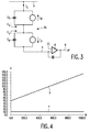
- Figure 3 is an equivalent circuit diagram for a pixel 2a.
- the photosensitive switching diode D1 is represented as a source of current I P in parallel with the capacitance C D while the photosensitive diode 3 is represented as a source of current 1 P in parallel with a capacitance C P .
- the photosensitive current I PHOTO is equal to KA C where K is a constant and A C is the area of the photosensitive diode which is exposed to light (normally this area is the area of the hole in the opaque electrode or contact of the photosensitive diode). Accordingly the condition for no leakage current can be defined by the geometry of the photosensitive diodes D1 and 3.
- equation 7 becomes: where A DD1 and A D3 are the areas of the switching diode D1 and photosensitive diode 3, respectively, and are thus proportional to their respective capacitances while A CD1 and A C3 are the areas of the switching diode D1 and photosensitive diode 3, respectively, exposed to incident light and are so proportional to the photocurrent generated by light incident on the respective diode.
- area in relation to the diodes D1 and 3 means the area of the diode in a plane generally parallel to the diode electrodes.
- the leakage current from an unselected pixel in the column of the selected pixel will flow internally within the capacitance/photocurrent loop of that unselected pixel and not through the column conductor 4, so eliminating or at least substantially reducing the vertical cross-talk.
- the areas of the contact holes (that is the areas exposed to light) of the two photosensitive diodes A CD1 and A C3 are equal, then, for zero vertical cross-talk, the area A D3 of the photodiode 3 should be the same as that A DD1 of the photosensitive switching diode D1.
- other relative geometies and dimensions may be possible which meet the conditions of equation 8.
- the photosensitive and switching diodes 3 and D1 may be reversed so as to have their anodes rather than their cathodes connected.
- Figure 4 illustrates graphically the effect of making the switching diodes D1 photosensitive.
- the vertical axis represents in arbitrary units the output A of the associated charge sensitive amplifier 8 when the selected pixel 2a is a dark pixel, that is the pixel has not been exposed to light since the previous reading out of that pixel 2a
- the horizontal axis represents the number N of unselected 'bright' pixels in the same column as the selected pixel, where the term 'bright pixel' means a pixel which is sensing light.
- the dotted line X in Figure 4 illustrates the output of the associated charge sensitive amplifier 8a when the switching diodes D1 of the column are not sensitive to light while the solid line Y in Figure 4 shows the output of the charge sensitive amplifier 8 when the switching diodes D1 of the column are photosensitive in accordance with the invention.
- the output of the charge sensitive amplifier 8 increases linearly with the number of illuminated pixels in the same column showing that leakage currents from unselected pixels in the same column are making a significant contribution to the current detected by the charge sensitive amplifier 8.
- the charge detected by the charge sensitive amplifier 8 of an imaging device in accordance with the invention does not change with the number of bright pixels 2a in the same column 8a showing that leakage current from those bright or illuminated pixels do not make any (or at least do not make any significant) contribution to the signal detected by the charge sensitive amplifier 8.
- the selected pixel 2a is correctly identified as being dark and is not swamped or obliterated by leakage currents from unselected pixels in the same column.
- the imaging device 1a shown in Figure 2 avoids or at least reduces the problems of vertical cross-talk, there is a possibility that, due to incomplete charging of the capacitances of the photosensitive diodes 3, there may be some "lag" in the image sensed. This should not present a problem where a stationary or slow moving image is being sensed but it could result in some blurring of the image if parts of the image are moving or changing rapidly.
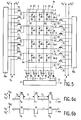
- Figure 5 illustrates an example of an imaging device 1b in accordance with the invention which additionally is designed to avoid or at least reduce such lag problems.
- each pixel or imaging element 2a incorporates a further rectifying element D2.
- Each rectifying element D2 is formed to be similar, generally identical, to the associated rectifying element D1 except that the rectifying elements D2 are not photosensitive.
- each pixel 2a The two rectifying elements D1 and D2 of each pixel 2a are coupled in series between second and third conductors 5 and 6 and the photosensitive diode 3 is coupled between the associated first conductor 4 and a junction J between the diodes D1 and D2.
- each diode D1 has its anode coupled to the associated second conductor 5 while each diode D2 has its cathode coupled to the associated third conductor 6.
- the photosensitive diodes 3 have their anodes coupled to the associated first or column conductor 4.
- two row driver arrangements 7a and 7b are used.
- the second conductors 5 are row conductors coupled via transistors 71 and 72 to a first shift register and decoder circuit 70a while the third conductors 6 are row conductors coupled via transistors 73 and 74 to a second shift register and decoder circuit 70b.
- the use of two such row driver arrangements 7a and 7b enables, as will be seen from the following, known row driving arrangements which are capably of supplying only two or three different voltages to be used.
- a pixel 2a of the imaging device 1b is read out by applying voltages to the row conductors 5 and 6 which will forward bias the associated switching diodes D1 and D2.
- Figures 6a and 6b illustrate graphically the charge in voltages V R1 and V R2 on the row conductors 5 and 6 respectively with time and illustrate the application at times t o , t1 and t2 of readout pulses R o , R1 and R2.
- the periods I o , I1, I2 between readout pulses are the integration periods during which the pixel concerned is storing charge representing any light incident on the pixel.
- the shift register and decoder circuits 70a and 70b render the associated transistors 71 and 73 conducting so that voltages V H + and V H ⁇ are supplied to the row conductors 5 and 6 so ensuring that the switching diodes D1 and D2 of that row are reverse-biassed.
- the shift register and decoder circuits 70a and 70b render the transistors 72 and 74 conducting so as to apply the voltages V S + and V S ⁇ to the row conductors 5 and 6, respectively, thereby ensuring that the switching diodes D1 and D2 of the selected pixel row are strongly forward biased allowing for rapid recharging of the capacitance of the photosensitive diode 3 of the selected row.
- Current will flow through the photosensitive diode 3 capacitance of the each selected pixel until the voltage at the associated junction J is reached. If the switching diodes D1 and D2 are identical (except in their ability to sense light) the voltage at the junction J will be the average of the voltages on the associated row conductors 5 and 6. At this stage, the pixel has reached its steady state and the read out is complete.
- the photosensitive diode 3 capacitance has thus been recharged within one read out period so avoiding the possibility of any lag.
- the conductors 6 may be coupled to a fixed reference potential and appropriate voltages supplied by the row driver arrangement 7a to render the switching diodes D1 and D2 forward or reverse biased as and when required.
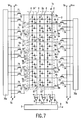
- FIG 7 illustrates another example of an imaging device 1c in accordance with the invention in which each pixel 2a comprises a further rectifying element D2. Although only an array of three columns and eight rows of pixels 2a is shown in Figure 7, it will be appreciated by those skilled in the art that the array may generally comprise a much larger number of rows and columns of pixels 2a.
- the third conductor 6a, 6b of each row of imaging elements 2a also forms the second conductor 5a, 5b of any adjacent rows of imaging elements 3, the first and second rectifying elements D1' and D2' of imaging elements 2a in alternate rows N-2, N, N+2, N+4, ... (N+2n, where n is an integer) being oppositely oriented to the first and second rectifying elements D1'' and D2'' of imaging elements 2a in the remaining rows N-1, +1, N+3, N+5 ... (N+(2n-1), where n is an integer) so that when forward-biased the first and second rectifying elements D1' and D2' of imaging elements 2a in the said alternate rows N, N+2, N+4, ...
- the switching diodes D1' and D2' in alternate rows N-2, N, N+2, N+4 ...(N+2n) are oriented so that the anodes of the first switching diodes D1' are coupled to the associated second conductor 5a while the cathodes of the switching diodes D2' are coupled to the associated third conductor 6b.
- the switching diodes D1'' and D2'' associated with the remaining rows N-1, N+1, N+3 ..(N+(2n-1)) of pixels 2a are oppositely oriented to the switching diodes D1' and D2' so that the cathodes of the switching diodes D1'' are coupled to the associated second conductor 5b while the anodes of the second switching diodes D2'' are coupled to the associated third conductor 6a.
- the photosensitive diodes 3 are oriented so that the cathode of each photosensitive diode 3 is coupled to the junction J between the corresponding first and second switching diodes D1 and D2.
- the third conductor 6b of the Nth row of pixels 2a forms the second conductor 5b of the N+1 row of pixels 2a while the third conductor 6a of the N+1 row of pixels 2a forms the second conductor 5a of the N+2 row of pixels 2a.
- Each of the row conductors 5a, 6a is coupled to voltage supply lines V+ and V- via respective switching transistors 71 and 72 of a first row driving circuit 7a.
- the gate or control electrodes of the switching transistors 71 and 72 are coupled to a shift register and decoder circuit 70a.
- a second row driving circuit 7b similarly comprises switching transistors 73 and 74 coupling the row conductors 5b, 6b to voltage supply lines Vo and V++, respectively, and having their control or gate electrodes coupled to a shift register and decoder circuit 70b.
- the shift register and decoder circuits 70a and 70b are again arranged to activate the appropriate transistors 71 to 74 under the control of clock signals in known manner to allow the appropriate voltage signals to be applied to the row conductors 5 and 6 at the appropriate times.
- the first or left row driving circuit 70a renders conducting the transistors 71 coupled to the row conductors 5a of the pixel rows N-2, N+2, N+4, ... and the transistor 72 coupled to the row conductor 5a of the pixel row N.
- the row conductor 5a of the pixel row N is coupled to the voltage supply line V+ while the row conductors 5a of the pixel rows N-2, N+2, N+4, ...(N+2n,where n ⁇ 0) are coupled to the voltage supply line V-.
- the second or right row driving circuit 70b renders conducting the transistors 73 coupled to the row conductors 5b of the pixel rows N+1, N+3, N+5, ...(N+(2n-1), where n ⁇ 0) and the transistor 74 coupled to the row conductor 5b of the pixel row N-1.
- the row conductor 5b of the pixel row N-1 is coupled to the voltage supply line V++ while the row conductors 5b of the pixel rows N+1, N+3, N+5, .. are coupled to the voltage supply line Vo.
- the voltage V++ is more positive than the voltage V+ which is itself more positive than the voltage Vo which is more positive than the voltage V-.
- the switching diodes D1' and D2' of the pixels 2a in the pixel row N are thus forward-biased while the switching diodes D1 and D2 of the pixels 2a of the pixel rows except the row N are reverse-biased.
- Current will flow through the photosensitive diode capacitances C of the pixels of the pixel row N to be integrated by the associated charge sensitive amplifier 8 which supplies an output signal to the output shift register and decoder circuit 9 from which image signals may be supplied by an output O to an appropriate store or to a display, neither of which is shown.
- Current flows through the photosensitive diode capacitances C of the pixels of the pixel row N until the average of the voltages of the two associated row conductors is reached.
- the photosensitive diode capacitance C can be completely recharged within the corresponding readout pulse and there is accordingly no, or at least considerably reduced, lag.
- the first or left row driving circuit 70a renders conducting the transistors 71 coupled to the row conductors 5a of the pixel rows N-2, N, N+4, ... (N+2n, where n ⁇ 1) and the transistor 72 coupled to the row conductor 5a of the pixel row N+2.
- the row conductor 5a of the pixel row N+2 is coupled to the voltage supply line V+ while the row conductors 5a of the pixel rows N-2, N, N+4, ... (N+2n, where n ⁇ 1) are coupled to the voltage supply line V-.
- the second or right row driving circuit 70b renders conducting the transistors 73 coupled to the row conductors 5b of the pixel rows N-1, N+1, N+5, .. (N+(2n-1), where n ⁇ 2) and the transistor 74 coupled to the row conductor 5b of the pixel row N+3.
- the row conductor 5b of the pixel row N+3 is coupled to the voltage supply line V++ while the row conductors 5b of the pixel rows N-1, N+1, N+5, .. are coupled to the voltage supply line Vo.
- the switching diodes D1 and D2 of the pixels 2a in the pixel row N+1 are thus forward-biased while the switching diodes D1 and D2 of the pixels 2a of the pixel rows except the row N+1 are reverse-biased.
- Current will flow through the photosensitive diode capacitances C of the pixels of the pixel row N+1 to be integrated by the associated charge sensitive amplifier 8 which supplies an output signal to the output shift register and decoder circuit 9 from which image signals may be supplied by an output O to an appropriate store or to a display, neither of which is shown.
- the image sensor 1 is formed using thin film technology on a suitable insulative substrate.
- the substrate should be transparent to that light.
- the row driver arrangements and charge sensitive amplifiers 8 and output shift register and decoder circuit 9 may be formed on separate substrates from (or around the periphery) of the array 2 and may, for example, be in the form of polycrystalline film transistor circuitry.
- Figure 8 shows one pixel of each of the adjacent rows N and N+1 and illustrates one possible schematic layout for one example of the image sensor shown in Figure 7 while Figure 9 illustrates a cross-sectional view taken along the line IX-IX in Figure 8 of a pixel 2a in the Nth one of the rows and Figure 10 illustrates a cross-sectional view taken along the line X-X of the two pixels 2a of the N and N+1 rows in the same column.
- a first electrically conductive layer is defined on an insulative, generally transparent, substrate 10, which may be formed of a suitable glass or plastics material, to form at least part of the row conductors 5, 6, the cathode electrodes 11a and 11b of the first switching diodes D1' and second switching diodes D2'' the cathode electrodes 12a and 12b of the second switching diodes D2' and first switching diodes D1' and the cathode electrodes 13 of the photosensitive diodes 3.
- the cathode electrodes 11a and 11b are formed integrally with the cathode electrode 13 of the associated photosensitive diode 3 while the cathode electrodes 12a and 12b are formed integrally with at least part of the associated row conductor 5b, 6b.
- the diodes 3, D1 and D2 are formed as amorphous silicon n-i-p diodes by depositing in sequence n conductivity, intrinsic conductivity and p conductivity amorphous silicon layers. These layers are then patterned to define the diode structures as shown in Figures 9 and 10. In the interests of simplicity, the diode structures are not shown cross-hatched in Figures 9 and 10.
- An insulating layer generally a silicon nitride layer, is then deposited and patterned to define dielectric isolation regions 14.
- a second electrically conductive layer again generally a chromium layer, is then deposited and patterned to define first interconnects 15a and 15b respectively coupling the anode of each first switching diode D1' and each second switching diode D2'' to the associated row conductor 5a,6a, second interconnects 16a and 16b respectively coupling the cathode of each first switching diode D1' to the anode of the associated second switching diode D2' and the cathode of each second switching diode D2'' to the anode of the associated first switching diode D1'' at least part of the column conductors 4.
- the layout structure of the pixels 2a of the remaining rows N-1, N+1, N+3, ... of the image sensor is effectively a mirror image of the pixels 2a of the rows N-2, N, N+2, except with respect to the interconnects, 15a and 16b which are defined to provide given areas A of the diodes D1' and D1'' which are exposed to light.
- the layout of the image sensor may have any appropriate pattern but, as shown in Figure 8, the row and column conductors 4 and 5, 6 define a rectangular, generally square grid with the switching diodes D1 and D2 and the photosensitive diodes 3 taking up as little area as possible of the pixels 2a to allow the image sensor to be as transparent as possible enabling the image sensor to be placed on top of something else such as a display without significantly obscuring the display.
- the areas of the photosensitive diodes 3 should be as large as possible.
- the above described structure enables all of the diodes D1, D2 and 3 to be formed as n-i-p rather than p-i-n diodes so enabling all of the diodes to be formed simultaneously.
- appropriate ones of the diodes may be formed as p-i-n diodes which should simply simplify the interconnection and metallisation patterns.
- the most suitable form of diode structure for the particular application will be used, it being borne in mind that generally n-i-p diodes are better photosensitive diodes than p-i-n diodes while p-i-n diodes are better switching diodes than n-i-p diodes.
- the switching diodes D2 differ from the photosensitive diodes 3 and photosensitive switching diodes D1 in that the anode and cathode electrodes of the switching diodes D2 shield the diodes from any incident light whereas the photosensitive diodes 3 and photosensitive switching diodes D1 are, as shown in Figures 9 and 10, exposed to light.
- the image sensor 1a may be manufactured in a similar manner so as to have a pixel layout similar to that of the pixel from row N shown in Figure 8 but with the diode D2 omitted, of course.
- the image sensor 1b may also have a similar layout to the pixel from row N shown in Figure 8 but of course each row of pixels would in that case have its own separate two row conductors.
- FIG 11 illustrates another example of an imaging device 1d.
- the imaging device 1d is similar to that shown in the example of Figures 7 to 10 except that, in this case, one of the two conductors associated with each row forms a row conductor 5a, 5b and the other 6a, 6b is provided by one of first and second reference conductors so that adjacent row conductors 5a, 5b are separated by a reference conductor 6a or 6b and each first reference conductor 6a is separated from any other first reference conductor 6a by two row conductors 5a, 5b and a second reference conductor 6b.
- the first and second rectifying elements D1' an D2' of storage elements 3 associated with a respective row conductor 5a, 5b are oppositely oriented to the first and second rectifying elements D1'' and D2'' of storage elements 3 associated with any adjacent row conductors 5b, 5a.
- the switching diodes D1' and D2' in each alternate pair A of rows N-1 and N, N+3 and N+4 ... are oriented so that the anodes of the first switching diodes D1' in the first row N-1, N+3... of the pair A are coupled to the first reference or common conductor 6a while the cathodes of the switching diodes D2' of that first row N-1, N+3... are coupled to the associated first row conductor 5a and to the anodes of the first switching diodes D1' in the second row N, N+4... of that pair A with the cathodes of the switching diodes D2' of the second row N, N+4... of that pair A being coupled to the second reference or common conductor 6b.
- the switching diodes D1'' and D2'' in the pair B of rows N+1 and N+2 adjacent the pair of rows N-1 and N (and N+5 and N+6 adjacent rows N+3 and N+4 and so on) are oriented so that the cathodes of the first switching diodes D1'' in the first row N+1, N+5... of the pair B are coupled to the second reference conductor 6b while the anodes of the switching diodes D2'' of that first row N+1, N+5... of that pair B are coupled to the associated second row conductor 5b and to the cathodes of the first switching diodes D1'' in the second row N+2, N+6... of that pair B with the anodes of the switching diodes D2'' of the second row N+2, N+6... of that pair B being coupled to the first reference conductor 6a.
- the photosensitive diodes 3 of the two rows in each pair of rows A or B are oppositely oriented to one another so that the photosensitive diodes 3' of the two rows (one from a pair of rows A and one from a pair of rows B) coupled to the same reference conductor 6a or 6b are oriented in the same direction.
- the photosensitive diodes 3' of rows N, N+1, N+4, N+5... are oriented so that the cathodes of the photosensitive diodes 3' are coupled to the junction or node J between the cathode of the associated first switching diode D1 and the anode of the associated second switching diode D2 while the anodes of the photosensitive diodes 3' are coupled to the associated column conductor 4.
- the photosensitive diodes 3'' in the remaining rows N-1, N+2, N+3, N+6.... are oriented so that the anodes of the photosensitive diodes 3'' are coupled to the junction or node J between the anode of the associated first switching diode D1 and the cathode of the associated second switching diode D2 while the cathodes of the photosensitive diodes 3'' are coupled to the associated column conductor 4.
- the means for supplying voltages comprises a row driving circuit arrangement 7a for supplying the appropriate voltages to the row conductors 5a and 5b and first and second reference voltage sources 7b and 7c for supplying the first and second reference voltages V- and V+, respectively.
- Each of the row conductors 5a, 5b is coupled to voltage supply lines V++, V0 and V-- via respective switching transistors 71, 72 and 73.
- the gate or control electrodes of the switching transistors 71, 72 and 73 are coupled to a shift register and decoder circuit 70.
- the shift register and decoder circuit 70 is arranged to activate the appropriate transistors 71, 72 and 73 under the control of clock signals in known manner to allow the appropriate voltage signals to be applied to the row conductors 5a and 5b at the appropriate times.
- each charge sensitive amplifier 8 is, for reasons which will be explained below, coupled to the output shift register and decoder circuit 9 by way of a full way rectifier 8a.
- the full wave rectifiers 8a may be of any suitable known form and are known simply as blocks in Figure 11.
- Figure 12 shows one pixel of each of the N-1 and N rows of one possible schematic layout for one example of the image sensor shown in Figure 11 while Figure 5 illustrates a cross-sectional view taken along the line XIII-XIII in Figure 12 of a pixel 2a in the Nth one of the rows and Figure 14 illustrates a cross-sectional view taken along the line XIV-XIV of the two pixels 2a of the N-1 and N rows in the same column.
- the first electrically conductive layer again generally a chromium layer, defined to form at least part of the row conductors 5a and 5b and the reference conductors 6a and 6b, the cathode electrodes 11a and 11b of the first switching diodes D1' of the N and N-1 rows, the cathode electrodes 12a and 12b of the second switching diodes D2' of the N and N-1 rows and the cathode electrodes 13 of the photosensitive diodes 3' and 3''.
- the cathode electrode 11a of the first switching diode D1' of the row N is formed integrally with the cathode electrode 13 of the associated photosensitive diode 3' while the cathode electrodes 12a and 12b are formed integrally with at least part of the associated reference conductor 6b and row conductor 5a.
- the second electrically conductive layer is then deposited and patterned to define first interconnects 15c and 15d respectively coupling the anode of the first switching diode D1' of the row N-1 to the associated reference conductor 6a and the anode of the first switching diode D1' of the row N to the associated row conductor 5a, a second interconnect 16c coupling the cathode of the photosensitive switching diode D1' of the row N-1 to the anode of the photosensitive diode 3'' and second interconnects 16d and 16e respectively coupling the anode of the photosensitive diode 3'' to the anode of the second switching diode D2' of the row N-1 and the anode of the second switching diode D2' of the row N to the cathode of the photosensitive diode 3', and at least part of the column conductors 4.
- the pixels 2a of the adjacent row N+1 of the image sensor have a similar structure to those of the row N but the actual orientation is reversed so that the pixels 2a of the row N+1 are a mirror image of the pixels 2a of the row N.
- the pixels 2a of the row N-2 of the image sensor have a similar structure to those of the row N-1 but the actual orientation is reversed so that the pixels 2a of the row N-2 are a mirror image of the pixels 2a of the row N-1, and so on.
- the pixels in adjacent rows but in different pairs A and B are effectively a mirror image of one another with the mirror being parallel to the reference conductor 6a or 6b separating the rows.
- the first common conductor 6a is held at a potential of V- while the second common conductor 6b is held at a potential of V+.
- the row driving circuit 70 renders conducting the transistor 73 coupled to the row conductor 5a of the pixel row N-1 and the transistors 71 coupled to the remaining row conductors 5a, 5b of the image sensor.
- the row conductor 5a of the pixel row N-1 is coupled to the voltage supply line V- while the remaining row conductors 5a, 5b are coupled to the voltage supply line V0.
- the switching diodes D1' and D2' of the pixels 2a in the pixel row N-1 are thus forward-biased while the switching diodes D1 and D2 of the pixels 2a of the pixel rows except the row N-1 are reverse-biased.
- the row driving circuit 70 renders conducting the transistor 72 coupled to the row conductor 5a of the pixel row N and the transistors 71 coupled to the remaining row conductors 5a, 5b of the image sensor.
- the row conductor 5a of the pixel row N is coupled to the voltage supply line V++ while the remaining row conductors 5a, 5b are coupled to the voltage supply line V0.
- the switching diodes D1'' and D2'' of the pixels 2a in the pixel row N are thus forward-biased while the switching diodes D1 and D2 of the pixels 2a of the pixel rows except the row N are reverse-biased.
- the row driving circuit 70 renders conducting the transistor 72 coupled to the row conductor 5b of the pixel row N+1 and the transistors 71 coupled to the remaining row conductors 5a, 5b of the image sensor.
- the row conductor 5b of the pixel row N+1 is coupled to the voltage supply line V++ while the remaining row conductors 5a, 5b are coupled to the voltage supply line V0.
- the switching diodes D1'' and D2'' of the pixels 2a in the pixel row N+1 are thus forward-biased while the switching diodes D1 and D2 of the pixels 2a of the pixel rows except the row N+1 are reverse-biased.
- the row driving circuit 70 renders conducting the transistor 73 coupled to the row conductor 5b of the pixel row N+2 and the transistors 71 coupled to the remaining row conductors 5a, 5b of the image sensor.
- the row conductor 5b of the pixel row N+2 is coupled to the voltage supply line V-- while the remaining row conductors 5a, 5b are coupled to the voltage supply line V0.
- the switching diodes D1' and D2' of the pixels 2a in the pixel row N+2 are thus forward-biased while the switching diodes D1 and D2 of the pixels 2a of the pixel rows except the row N+2 are reverse-biased.
- the charge stored at every fourth (for example the Nth, N+4th, N+8th etc.) row of pixels is readout in the same way, although, of course, generally the rows will be read in sequence.
- the photosensitive diode capacitances C can be completely recharged within the corresponding readout pulse and there is accordingly no lag. This means that if the noise associated with the image sensor is low, the image sensor can operate in low-light conditions without excessive lag problems. Also, it should be possible to read the pixels more quickly because the switching diodes D1 and D2 of the selected pixel row are strongly forward biased and are able to recharge the pixel capacitances quickly.
- the image sensor should exhibit very little vertical cross-talk, that is interference between column conductors, because such cross-talk is a function of the time for which a pixel row is selected and the frame time and in the present case, the row select time can be reduced.
- the fact that the number of row conductors is half that of a conventional image sensor such as that shown in Figure 1 and a quarter that of the device shown in Figure 5 means that an image sensor in accordance with the present invention is particularly suitable for mounting on a common substrate with other similar image sensors in the manner described in EP-A-555907 because of the resulting larger separation of the row conductors.
- each row of pixels may thus be read in sequence by applying the appropriate voltages to the appropriate row conductors 5a and 5b.
- the remaining pixels have their associated switching diodes D1 and D2 reverse-biased and accordingly these pixels are in their integration period in which charge resulting from the photo-generation of charge carriers within the photosensitive diode by any light incident on the pixel is stored at the pixel.
- the charge stored at a row of pixels during the integration period is read out in the subsequent read out period and the rows of pixels are read out sequentially.
- FIG. 15 shows one pixel 20 of an image sensor 1b, 1c or 1d where Figure 16 is an equivalent circuit diagram for a pixel of row N in any of Figures 5, 7 and 11.
- the photosensitive switching diode D1 is represented as a source of current I D in parallel with the capacitance C x while the photosensitive diode 3 is represented as a current of current I P in parallel with the capacitance C P .
- the non-photosensitive switching diode D2 is represented simply as the capacitance C y in parallel with the capacitance C x because it of course is not responsive to incident light.
- the photosensitive current I PHOTO is equal to KA CON where K is a constant and A CON is the area of the photodiode which is exposed to light (normally this area is the area of the hole in the opaque electrode or contact of the photodiode, for example the electrode 4 in Figure 9). Accordingly the condition for no leakage current can again be defined by the geometry of the photosensitive diodes D1 and 3'.
- equation 14 becomes: where A DD1 and A D3 are the areas of the switching diode D1 and photosensitive diode 3, respectively, and are thus proportional to their capacitance while A CD1 and A C3 are the areas of the switching diode D1 and photosensitive diode 3, respectively, exposed to incident light and are so proportional to the photocurrent generated by light incident on the respective diode.
- the term "area" in relation to the diodes D1, D2 and 3 means the area of the diode in a plane generally parallel to the diode electrodes, that is, in relation to Figures 9 and 10, for example, in a plane parallel to the surface of the substrate 10 upon which the diodes are formed. The thicknesses of the diodes are measured in a direction perpendicular to the surface of the substrate 10.
- the leakage current from an unselected pixel in the column of the selected pixel will flow internally within the capacitance/photocurrent loop of that unselected pixel and not through the column conductor 4, so eliminating or at least substantially reducing the vertical cross-talk.
- the area of the photodiode 3 should be twice that of the photosensitive switching diode D1.
- the row, common and column conductors need not necessarily extend horizontally and vertically as shown in the drawings. Indeed, the row and common conductors may extend vertically while the column conductors extend horizontally, that is the device as shown may be rotated through 90°. Also, the row, common and column conductors need not necessarily be perpendicular to one another, any suitable arrangement may be used.
- the term "rectifying element” means any element which has an asymmetric characteristic and passes as low a current as possible in one direction (the reverse direction) and the required current in the other direction (the forward direction).
- the rectifying elements need not necessarily be diodes but could be any suitable form of, generally two-terminal, rectifying element.
- the photosensitive elements need not necessarily be diodes but could be other types of photosensitive device which pass current when illuminated.
- the photosensitive diodes could be replaced by photoconductors, for example formed of lead oxide, each in series with an appropriate capacitance.
Landscapes
- Engineering & Computer Science (AREA)
- Multimedia (AREA)
- Signal Processing (AREA)
- Transforming Light Signals Into Electric Signals (AREA)
- Solid State Image Pick-Up Elements (AREA)
Applications Claiming Priority (2)
| Application Number | Priority Date | Filing Date | Title |
|---|---|---|---|
| GB9404115A GB9404115D0 (en) | 1994-03-03 | 1994-03-03 | An imaging device |
| GB9404115 | 1994-03-03 |
Publications (2)
| Publication Number | Publication Date |
|---|---|
| EP0670656A2 true EP0670656A2 (de) | 1995-09-06 |
| EP0670656A3 EP0670656A3 (de) | 1996-02-28 |
Family
ID=10751238
Family Applications (1)
| Application Number | Title | Priority Date | Filing Date |
|---|---|---|---|
| EP95200467A Withdrawn EP0670656A3 (de) | 1994-03-03 | 1995-02-24 | Bildaufnahmevorrichtung. |
Country Status (4)
| Country | Link |
|---|---|
| US (1) | US5608205A (de) |
| EP (1) | EP0670656A3 (de) |
| JP (1) | JPH07264485A (de) |
| GB (1) | GB9404115D0 (de) |
Cited By (2)
| Publication number | Priority date | Publication date | Assignee | Title |
|---|---|---|---|---|
| EP1061732A1 (de) * | 1999-06-15 | 2000-12-20 | Commissariat A L'energie Atomique | Verfahren zur durch ihre zugehörigen Dioden/Photodioden Polarisierung der Photodioden eines Matrixsensors |
| EP2164103A1 (de) * | 2008-09-08 | 2010-03-17 | Sehyun Co., Ltd. | Bildsensor und Verfahren zu dessen Herstellung |
Families Citing this family (10)
| Publication number | Priority date | Publication date | Assignee | Title |
|---|---|---|---|---|
| US6201573B1 (en) * | 1995-11-13 | 2001-03-13 | Hamamatsu Photonics K. K. | Solid state imaging apparatus for imaging a two dimensional optical image having a number of integration circuits |
| GB9620762D0 (en) * | 1996-10-04 | 1996-11-20 | Philips Electronics Nv | Charge measurement circuit |
| FR2760585B1 (fr) * | 1997-03-07 | 1999-05-28 | Thomson Tubes Electroniques | Procede de commande d'un dispositif photosensible a faible remanence, et dispositif photosensible mettant en oeuvre le procede |
| FR2796239B1 (fr) * | 1999-07-06 | 2001-10-05 | Trixell Sas | Procede de commande d'un dispositif photosensible apte a produire des images de bonne qualite |
| US6621887B2 (en) * | 2001-10-15 | 2003-09-16 | General Electric Company | Method and apparatus for processing a fluoroscopic image |
| US6920198B2 (en) | 2003-05-02 | 2005-07-19 | Ge Medical Systems Global Technology Company, Llc | Methods and apparatus for processing a fluoroscopic image |
| JPWO2006112320A1 (ja) * | 2005-04-15 | 2008-12-11 | 株式会社日立メディコ | X線平面検出器及びx線画像診断装置 |
| KR101415725B1 (ko) * | 2008-05-21 | 2014-07-21 | 서울대학교산학협력단 | 표시 장치와 그 구동 방법 |
| US20120049041A1 (en) * | 2010-09-01 | 2012-03-01 | International Business Machines Corporation | Switched rail circuitry and modified cell structure and method of manufacture and use |
| US20160003672A1 (en) * | 2014-07-25 | 2016-01-07 | Varun Verma | Multiplexer for single photon detector, process for making and use of same |
Family Cites Families (12)
| Publication number | Priority date | Publication date | Assignee | Title |
|---|---|---|---|---|
| JPS5856363A (ja) * | 1981-09-30 | 1983-04-04 | Hitachi Ltd | 受光素子 |
| DE3478779D1 (en) * | 1983-02-15 | 1989-07-27 | Sharp Kk | Two-dimensional image readout device |
| US4728802A (en) * | 1986-01-21 | 1988-03-01 | Ovonic Imaging Systems, Inc. | Balanced drive photosensitive pixel and method of operating the same |
| FR2605166B1 (fr) * | 1986-10-09 | 1989-02-10 | Thomson Csf | Dispositif photosensible a l'etat solide, procede de lecture et procede de fabrication |
| FR2626127B1 (fr) * | 1988-01-15 | 1990-05-04 | Thomson Csf | Matrice photosensible a trois diodes par point, sans remise a niveau |
| FR2627923B1 (fr) * | 1988-02-26 | 1990-06-22 | Thomson Csf | Matrice d'elements photosensibles et detecteur de radiations comportant une telle matrice, notamment detecteur de rayons x a double energie |
| FR2634947B1 (fr) * | 1988-07-29 | 1990-09-14 | Thomson Csf | Matrice photosensible a deux diodes de meme polarite et une capacite par point photosensible |
| FR2636800A1 (fr) * | 1988-09-16 | 1990-03-23 | Thomson Csf | Procede de lecture de cellules photosensibles du type comportant deux diodes montees en serie avec des sens de conduction opposes |
| US5410349A (en) * | 1990-07-06 | 1995-04-25 | Fuji Photo Film Co., Ltd. | Solid-state image pick-up device of the charge-coupled device type synchronizing drive signals for a full-frame read-out |
| GB9202693D0 (en) * | 1992-02-08 | 1992-03-25 | Philips Electronics Uk Ltd | A method of manufacturing a large area active matrix array |
| US5376782A (en) * | 1992-03-04 | 1994-12-27 | Fuji Xerox Co., Ltd. | Image pickup device providing decreased image lag |
| GB9308543D0 (en) * | 1993-04-24 | 1993-06-09 | Philips Electronics Uk Ltd | An image sensor |
-
1994
- 1994-03-03 GB GB9404115A patent/GB9404115D0/en active Pending
-
1995
- 1995-02-24 EP EP95200467A patent/EP0670656A3/de not_active Withdrawn
- 1995-03-03 US US08/398,324 patent/US5608205A/en not_active Expired - Fee Related
- 1995-03-03 JP JP7044233A patent/JPH07264485A/ja active Pending
Cited By (4)
| Publication number | Priority date | Publication date | Assignee | Title |
|---|---|---|---|---|
| EP1061732A1 (de) * | 1999-06-15 | 2000-12-20 | Commissariat A L'energie Atomique | Verfahren zur durch ihre zugehörigen Dioden/Photodioden Polarisierung der Photodioden eines Matrixsensors |
| FR2795271A1 (fr) * | 1999-06-15 | 2000-12-22 | Commissariat Energie Atomique | Procede de polarisation des photodiodes d'un capteur matriciel par leurs pixels connexes |
| US6707497B1 (en) | 1999-06-15 | 2004-03-16 | Commissariat A L'energie Atomique | Method of biasing the photodiodes of a matrix sensor through associated pixels thereof |
| EP2164103A1 (de) * | 2008-09-08 | 2010-03-17 | Sehyun Co., Ltd. | Bildsensor und Verfahren zu dessen Herstellung |
Also Published As
| Publication number | Publication date |
|---|---|
| US5608205A (en) | 1997-03-04 |
| GB9404115D0 (en) | 1994-04-20 |
| EP0670656A3 (de) | 1996-02-28 |
| JPH07264485A (ja) | 1995-10-13 |
Similar Documents
| Publication | Publication Date | Title |
|---|---|---|
| US5721422A (en) | Electronic devices having an array with shared column conductors | |
| US4810881A (en) | Panel for X-ray photography and method of manufacture | |
| EP0509589B1 (de) | Optisches Berührungseingabegerät | |
| EP0603972A1 (de) | Bildvorrichtung mit einem elektrostatischen Schutznetz | |
| EP0670656A2 (de) | Bildaufnahmevorrichtung | |
| CA1324210C (en) | Balanced drive photosensitive pixel and method of operating the same | |
| CA1080345A (en) | Semiconductor optical image sensing device | |
| US6980243B2 (en) | Photoelectric conversion device providing advantageous readout of two-dimensional array of transistors | |
| US4583002A (en) | Imaging sensor with automatic sensitivity control comprising voltage multiplying means | |
| EP0577391A2 (de) | Festkörperbildaufnahmevorrichtung | |
| US5426292A (en) | Image sensor having a two dimensional array of imaging elements with opposite polarity leakage currents | |
| US4495409A (en) | Photosensor with diode array | |
| US4857751A (en) | Photoelectric conversion apparatus with separating electrodes | |
| US5572015A (en) | Charge storage device having shared conductors | |
| JPS6386973A (ja) | 露光ブロツキング素子をもつ感光ピクセル | |
| US5856666A (en) | Multiplexer circuit | |
| US5569908A (en) | Charge storage device having shared conductors | |
| KR100434005B1 (ko) | 영상 감지기 | |
| JPS6237812B2 (de) | ||
| US5572255A (en) | Image reading apparatus and method for driving appropriate photoelectric energy converting elements when first and second driving voltages are applied simultaneously | |
| US5539458A (en) | TFT-drive image sensor capable of producing an offset-free image signal | |
| JPS61242068A (ja) | イメ−ジセンサ | |
| US4916326A (en) | Long array photoelectric converting apparatus with reduced crosstalk | |
| Schulte et al. | Intelligent image sensor for on-chip contour extraction | |
| JP2699895B2 (ja) | イメージセンサの駆動方法 |
Legal Events
| Date | Code | Title | Description |
|---|---|---|---|
| PUAI | Public reference made under article 153(3) epc to a published international application that has entered the european phase |
Free format text: ORIGINAL CODE: 0009012 |
|
| AK | Designated contracting states |
Kind code of ref document: A2 Designated state(s): DE FR GB IT NL |
|
| PUAL | Search report despatched |
Free format text: ORIGINAL CODE: 0009013 |
|
| AK | Designated contracting states |
Kind code of ref document: A3 Designated state(s): DE FR GB IT NL |
|
| 17P | Request for examination filed |
Effective date: 19960828 |
|
| 17Q | First examination report despatched |
Effective date: 19980806 |
|
| STAA | Information on the status of an ep patent application or granted ep patent |
Free format text: STATUS: THE APPLICATION IS DEEMED TO BE WITHDRAWN |
|
| 18D | Application deemed to be withdrawn |
Effective date: 19990217 |