EP0670568A1 - Display device - Google Patents
Display device Download PDFInfo
- Publication number
- EP0670568A1 EP0670568A1 EP95301411A EP95301411A EP0670568A1 EP 0670568 A1 EP0670568 A1 EP 0670568A1 EP 95301411 A EP95301411 A EP 95301411A EP 95301411 A EP95301411 A EP 95301411A EP 0670568 A1 EP0670568 A1 EP 0670568A1
- Authority
- EP
- European Patent Office
- Prior art keywords
- power supply
- driver
- display device
- voltage
- column
- Prior art date
- Legal status (The legal status is an assumption and is not a legal conclusion. Google has not performed a legal analysis and makes no representation as to the accuracy of the status listed.)
- Granted
Links
Images


Classifications
-
- G—PHYSICS
- G09—EDUCATION; CRYPTOGRAPHY; DISPLAY; ADVERTISING; SEALS
- G09G—ARRANGEMENTS OR CIRCUITS FOR CONTROL OF INDICATING DEVICES USING STATIC MEANS TO PRESENT VARIABLE INFORMATION
- G09G3/00—Control arrangements or circuits, of interest only in connection with visual indicators other than cathode-ray tubes
- G09G3/20—Control arrangements or circuits, of interest only in connection with visual indicators other than cathode-ray tubes for presentation of an assembly of a number of characters, e.g. a page, by composing the assembly by combination of individual elements arranged in a matrix no fixed position being assigned to or needed to be assigned to the individual characters or partial characters
- G09G3/34—Control arrangements or circuits, of interest only in connection with visual indicators other than cathode-ray tubes for presentation of an assembly of a number of characters, e.g. a page, by composing the assembly by combination of individual elements arranged in a matrix no fixed position being assigned to or needed to be assigned to the individual characters or partial characters by control of light from an independent source
- G09G3/36—Control arrangements or circuits, of interest only in connection with visual indicators other than cathode-ray tubes for presentation of an assembly of a number of characters, e.g. a page, by composing the assembly by combination of individual elements arranged in a matrix no fixed position being assigned to or needed to be assigned to the individual characters or partial characters by control of light from an independent source using liquid crystals
- G09G3/3611—Control of matrices with row and column drivers
- G09G3/3622—Control of matrices with row and column drivers using a passive matrix
- G09G3/3625—Control of matrices with row and column drivers using a passive matrix using active addressing
-
- G—PHYSICS
- G09—EDUCATION; CRYPTOGRAPHY; DISPLAY; ADVERTISING; SEALS
- G09G—ARRANGEMENTS OR CIRCUITS FOR CONTROL OF INDICATING DEVICES USING STATIC MEANS TO PRESENT VARIABLE INFORMATION
- G09G2330/00—Aspects of power supply; Aspects of display protection and defect management
- G09G2330/02—Details of power systems and of start or stop of display operation
Abstract
Description
- The present invention relates to a display device which drives a simple matrix type liquid crystal panel. In more detail, it relates to a display device which drives a liquid crystal panel by multi line selection addressing. In still further detail, it relates to a power supply structure with respect to a common driver and segment driver included in the display device.
- Simple matrix type liquid crystal panels support a liquid crystal layer between row electrodes and column electrodes and provide pixels in matrix form at the crossing points of the row and column electrodes. Conventionally, the liquid crystal panel is driven by a voltage averaging method. This method selects one row electrode at a time in sequence, and imparts data signals corresponding to an ON/OFF to all column electrodes in accordance with a selected timing. As a result, the voltage applied to each pixel serves as a high application voltage once (for a 1/N time period) during one frame interval which selects all the row electrodes (N electrodes) in turn, and for the remaining time period ((N-1)/N) during one frame interval serves as a constant bias voltage. When the response speed of the liquid crystal material used is slow, a change of brightness according to the effective value of the application voltage waveform during one frame interval can be obtained. Consequently, when a frame frequency taking a large division number, large number of row electrodes, decreases, the difference between one frame interval and the response time of the liquid crystal becomes small. As a result, the liquid crystal response for each applied pulse is reduced, and contrast changes occur in which flickering of the brightness appears. This is known as "frame response".
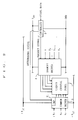
- A "Multi Line Selection Addressing Method" has been proposed as a manner of dealing with the problem of frame response, and is disclosed in, for example, Published Japanese Patent Application 5-100642. One example of a display device using a liquid crystal panel driven by this method is shown in Fig. 8. This multi line selection addressing method, by selecting a number of row electrodes simultaneously rather than conventional selection of one row electrode at a time line by line, operates at a lower frame interval (executes visible high frequency) and so suppresses the above-described frame response. Since it selects a number of row electrodes simultaneously rather than selecting line by line, a means is required to obtain arbitrary pixel display. In other words, it is necessary to perform a calculation process on the original pixel data and supply appropriate voltages to the column electrodes. Specifically, as well as providing a
controller 101 and producing orthonormal signals represented by a set of orthonormal functions, thecontroller 101 produces a sum of products signal in accordance with a result of performing a sum of products calculation with a set of the orthonormal functions and a set of selected pixel data. Acommon driver 102 applies a row driving waveform having a predetermined voltage level (+Vr, Vo, -Vr) to the row electrodes of aliquid crystal panel 103 by group sequential scanning in each selection time period, according to the orthonormal signals. Meanwhile, asegment driver 104 applies a column driving waveform having a predetermined voltage (V₁, V₂, ... Vn-1, Vn) to the column electrodes of theliquid crystal panel 103 in synchronisation with the group sequential scanning, according to the sum of products signals. - To continue, the problems of conventional techniques will be briefly explained with reference to Fig. 8. Generally, while the
common driver 102 andsegment driver 104 for driving theliquid crystal panel 103 output a driving waveform of relatively high voltage level, thecontroller 101 performs only control with respect to thecommon driver 102 and thesegment driver 104 and operates within a low voltage range in the same way as a normal IC. Due thereto, the conventionalcommon driver 102 andsegment driver 104 are connected with high voltage power supply order (+VLC, -VLC), and thecontroller 101 is connected with low voltage power supply order (VDD, GND). Thecommon driver 102 andsegment driver 104 are formed by high voltage withstanding ICs, and thecontroller 101 is formed by a low voltage withstanding IC. - Incidentally, the voltage level of the row driving waveform output by the
common driver 102 and the voltage level of the column driving waveform output by thesegment driver 104 do not include mutually equal voltage ranges, but change in dependence on and relative to the main number of row electrodes simultaneously selected in each selection time interval. Where the simultaneously selected main number is small compared to total number (total main number) of row electrodes the range of voltage levels on thecommon driver 102 side becomes relatively wide and the range of voltage levels on thesegment driver 104 side becomes narrow. Conversely, where the simultaneously selected main number becomes relatively large with respect to the total number of row electrodes, the range of voltage levels on thecommon driver 102 side becomes narrow and the range of voltage levels on thesegment driver 104 side becomes wide. In spite of the range of required voltage levels of thecommon driver 102 and thesegment driver 104 differing in this way, because both conventional drivers are supplied in common by a high voltage power supply, high voltage withstanding structure ICs have been used for both. For example, with respect to thecontroller 101 being able to use a normal IC having a withstandable voltage rating in the vicinity of 5V, the driver ICs required a withstandable voltage rating in the range of 30V. In manufacturing this type of high voltage withstanding IC special structures and processes are required, which is a problem from the financial aspect. For example, with a high voltage withstanding IC special processes such as thickening the gate insulation film, etc. are performed. Also, special structures such as a double-layer diffusion drain and lengthened gate lengths etc. are employed to raise the withstandable voltage. The result of this is that the chip size is enlarged and the cost raised by the increase in manufacturing processes. Further, it is disadvantageous due to the increase in current consumption accompanying the raising of the power supply voltage, increased generation of noise, and the like. - This invention was produced in an attempt to overcome the above problem, at least in part.
- This invention provides a display device for driving a liquid crystal display having row electrodes and column electrodes and comprising:
a column driver for applying row driving waveforms to the row electrodes by group sequential scanning;
a segment driver for applying a column driving waveform to the column electrodes, and characterised by
the common driver and segment driver being driven by different power supply voltages. - This invention also provides a display device for driving, in accordance with pixel data, a liquid crystal panel which supports liquid crystal between column electrodes and row electrodes and is provided with pixels in a matrix form, the display device comprising:
a controller for, as well as producing orthonormal signals represented by a set of orthonormal functions, producing sum of products signals in accordance with a result of performing a sum of products calculation with a set of the orthonormal functions and a set of picel data;
a common driver for applying row driving waveforms having a predetermined voltage level to the row electrodes by group sequential scanning at selected intervals in accordance with the orthonormal signals; and
a segment driver for applying column driving waveforms having a predetermined voltage level to the column electrodes in synchronisation with the group sequential scanning in accordance with the sum of products signals, wherein
the common driver and segment driver are driven buy different power supply voltages (+VLC, -VLC, VDD and GND). - This invention further provides a display device for driving, in accordance with pixel data, a liquid crystal panel which supports liquid crystal between column electrodes and row electrodes and is provided with pixels in a matrix form, the display device comprising:
a controller for, as well as producing orthonormal signals represented by a set of orthonormal functions, producing a sum of product signals in accordance with a result of performing a sum of product calculation with a set of the orthonormal functions and a set of pixel data;
a common driver for applying row driving waveforms having a predetermined voltage level to the row electrodes by group sequential scanning at selected intervals in accordance with the orthonormal signals; and
a segment driver for applying column driving waveforms having a predetermined voltage level to the column electrodes in synchronisation with the group sequential scanning in accordance with the sum of product signals, wherein
the common driver and segment driver are driven by different power supply voltages. - The following means were devised to solve the problems of the prior art techniques described above. Namely, the display device of the present invention includes a liquid crystal panel supporting a liquid crystal layer between row electrodes and column electrodes and provides matrix form pixels, and multi line selection addressing drives in accordance with input pixel data. Therefore, as well as the liquid crystal panel, it has a controller, a common driver and a segment driver. The controller, as well as producing orthonormal signals represented by set of orthonormal functions, produces a sum of product signals in accordance with a result of performing a sum of product calculation with a set of the orthonormal signals and a set of the pixel data. The common driver applies a row driving waveform having a predetermined voltage level to the row electrodes by group sequential scanning at selected intervals in accordance with the orthonormal signals. The segment driver applies a column driving waveform having a predetermined voltage level to the column electrodes in synchronisation with the group sequential scanning and in accordance with the sum of product signals. In this inventive type of structure, the common driver and segment driver are characterised by being separately supplied by a pair of power supplies having different power supply voltages.
- In one feature of the present invention, while the common driver is supplied by a high voltage power supply and outputs a row driving waveform of relatively high voltage level, the segment driver is supplied by a low voltage power supply and outputs a column driving waveform of relatively low voltage level. For example, while the high voltage power supply has a power supply voltage surpassing 10V, the low voltage power supply has a power supply voltage not surpassing 10V. Further, the controller can be supplied with power by a low voltage power supply in common with the segment driver. In this case, the low voltage power supply has a power supply voltage in the vicinity of 5V in line with the voltage rating of the controller. Preferably, the segment driver outputs a column driving waveform having a voltage falling within a range in the vicinity of 5V, the common driver should perform group sequential scanning of groups of 15 or less row electrodes simultaneously as one set. For example, the common driver performs group sequential scanning of 6 line electrodes simultaneously as one set. According to another feature of the present invention, a central potential of a power supply voltage output by the high voltage power supply and a central potential of a power supply voltage output by the low voltage power supply are both substantially in agreement. Also, it includes a voltage level circuit, which resistively divides a power supply voltage output by the high voltage power supply to produce a plurality of voltage levels, and supplies it to the segment driver and uses it in forming the column driving waveform. In addition, it includes a level shifter and level shifts the orthogonal signal output from the controller connected to the low voltage power supply to input it to the common driver connected to the high voltage power supply.
- Alternatively, in place thereof, the common driver connected to the high voltage power supply side can incorporate an input comparator, and can directly receive the orthonormal signal output from the controller connected to the low voltage power supply side.
- A display device employing the invention will now be described by way of example only with reference to the accompanying diagrammatic figures in which;
- Fig. 1 is a block drawing showing the basic structure of a display device according to the present invention;
- Fig. 2 is a block drawing showing a variation of the display device shown in Fig. 1;
- Fig. 3 is a circuit diagram showing a more detailed concrete structural example of the display device shown in Fig. 1;
- Fig. 4 is a timing chart which accompanies an explanation of the operation of the display device shown in Fig. 3;
- Fig. 5 is a wave form chart which similarly accompanies an explanation of the operation of the display device shown in Fig. 3;
- Fig. 6 is a circuit diagram showing a structural example of a voltage level circuit incorporated in the display device shown in Fig. 3;
- Fig. 7 is a voltage level chart which accompanies an explanation of the operation of the voltage level circuit shown in Fig. 6; and
- Fig. 8 is a block drawing showing an example of a conventional display device.
- According to the present invention, the common driver and segment driver are separately supplied by a pair of power supplies having different power supply voltages. In other words, according to the voltage level of the row driving waveform output from the common driver and the voltage level of the column driving waveform output from the segment driver, separate power sources having appropriate power supply voltages are separately prepared and connected to the common driver and the segment driver. For example, the common driver is connected to a high voltage power supply and the segment driver is connected to a low voltage power supply. By means of this type of structure, it becomes possible to employ at least one driver which only needs to withstand a low voltage and as a result an IC produced by normal processing can be used. Further, if the controller is connected to a common low voltage power supply with the segment driver, the circuit structure can be simplified. For example, it is permissible to connect in common a controller and segment driver having a withstandable voltage rating in the vicinity of 5V to a low voltage power supply, (low voltage power supply side).
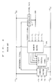
- Below, preferred embodiments of the present invention will be explained in detail with reference to the drawings. Fig. 1 is a block drawing showing the basic structure of a display device according to the present invention. As shown in Fig. 1, this display device is formed from a
liquid crystal panel 1, acontroller 2, acommon driver 3, asegment driver 4, alevel shifter 5, and so on. Theliquid crystal panel 1 supports a liquid crystal layer between row electrodes and column electrodes and provides pixels in a matrix form. Thecontroller 2, as well as producing an orthonormal signal represented by a set of orthonormal functions, produces a sum of products signal in accordance with a result of performing a sum of products calculation with a set of the orthonormal functions and a set of pixel data. Thecommon driver 3 is connected to thecontroller 2 via thelevel shifter 5, and applies a row driving waveform having a predetermined voltage level (+Vr, Vo, -Vr) to the row electrodes of theliquid crystal panel 1 by group sequential scanning of a predetermined number of row electrodes at a time at selected intervals, in accordance with the orthonormal signals. Meanwhile, thesegment driver 4 applies a column driving waveform having a predetermined voltage level (V₁, V₂, ... Vn-1, Vn) to the column electrodes of theliquid crystal panel 1 in synchronisation with the group sequential scanning, in accordance with the sum of products signal. - As a feature of the present invention, the
common driver 3 and thesegment driver 4 are separately supplied by a pair of power supplies having different power supply voltages. In the present embodiment, thecommon driver 3 is supplied by a high voltage power supply (+VLC, -VLC) and outputs a relatively high voltage level row driving waveform. Meanwhile, thesegment driver 4 is supplied by a low voltage power supply (VDD, GND) and outputs a relatively low voltage level column driving waveform. In the present embodiment, while the high voltage power supply (+VLC, -VLC) has a power supply voltage surpassing 10V, the low voltage power supply (VDD, GND) has a power supply voltage not surpassing 10V. Thecontroller 2 is supplied by the low voltage power supply (VDD, GND) in common with thesegment driver 4. Thecontroller 2 is formed by an IC rated to withstand, for example, a voltage of 5V. Similarly, the segment driver is also formed by an IC rated to withstand a voltage of 5V. Accordingly, the low voltage power supply (VDD, GND) has a power supply voltage in the vicinity of 5V in keeping with the voltage withstanding rating of these ICs. With this relationship, thesegment driver 4 outputs a column driving waveform which combines a plurality of voltage levels (V₁, V₂, ... Vn-1, Vn) falling within a range in the vicinity of 5V based on a sum of products signal. On the other hand, thecommon driver 3 performs group sequential scanning of 15 or less row electrodes as one set so as to satisfy the condition relating to the voltage level on thesegment driver 4 side. For example, thecommon driver 3 performs group sequential scanning of 6 row electrodes as one set. In this case the voltage level (+Vr, Vo, -Vr) of the row driving waveform output by thecommon driver 3 side falls under 30V, and the power supply voltage of the high voltage power supply (+VLC, -VLC) is set in the vicinity of 30V. - In the display device of the present embodiment, a central potential of a power supply voltage output by the high voltage power supply (+VLC, -VLC) and a central potential of a power supply voltage output by the low voltage power supply (VDD, GND) are both substantially in agreement. Further, the display device includes a voltage level circuit (not shown in Fig. 1) which, as well as supplying a predetermined voltage level (+Vr, Vo, -Vr) to be used by the
common driver 3 in synthesising the row driving waveform, supplies a predetermined voltage level (V₁, V₂, ... Vn-1, Vn) to be used by thesegment driver 4 in synthesising the column driving waveform. This voltage level circuit resistively divides the power supply voltage output from the high voltage power supply to produce the plurality of voltage levels (+Vr, Vo, -Vr, V₁, V₂, ... Vn-1, Vn) used by thesegment driver 4 and thecommon driver 3. Accordingly, it is very easy to make the central potential of the row driving waveform output from thecommon driver 3 and the central potential of the column driving waveform output from thesegment driver 4 conform, and complete alternating current driving of theliquid crystal panel 1 can be realised. - Lastly, the
level shifter 5 described above level shifts the orthonormal signal output from thecontroller 2 of the low voltage power supply side to input it to thecommon driver 3 on the high voltage power supply side. In the present embodiment the power supply of thecontroller 2 and the power supply of thecommon driver 3 are separate and independent. Consequently thelevel shifter 5 is used and level adjusting of the orthonormal signals is necessary. In other words, it is permissible to shift the level of the orthonormal signals so as to align it with the logic operation level in the interior of thecommon driver 3. - Fig. 2 is a block drawing showing an example of a variation of the display device shown in Fig. 1. The basic structure is the same as the display device shown in Fig. 1, and corresponding reference numbers are attached to corresponding parts for ease of understanding. A difference is that a comparator (CMP) 31 is incorporated in the input stage of the
common driver 3 instead of employing aseparate level shifter 5. Thecomparator 31 enables direct reception of the orthonormal signal output from thecontroller 2 on the low voltage power supply side. In other words, thecomparator 31 provides a threshold level in agreement with a central level of the orthonormal signals, and converts an amplitude in the vicinity of 5V to an amplitude in the vicinity of 30V. This conversion can be carried out by thecomparator 31 or by thecommon driver 3. - Fig. 3 is a circuit diagram showing a more detailed concrete structural example of the display device shown in Fig. 1. As shown in Fig. 3, the present display device provides a simple matrix type
liquid crystal panel 1. Thisliquid crystal panel 1 has a flat panel structure which interleaves a liquid crystal layer between therow electrodes 11 and thecolumn electrodes 12. As the liquid crystal layer an STN liquid crystal for example can be used. Thecommon driver 3 is connected to therow electrodes 11 to drive them. Also thesegment driver 4 is connected to thecolumn electrodes 12 to drive them. - The
controller 2 comprises aframe memory 21, an orthonormal, or orthogonal,function generating circuit 22 and a sum ofproducts calculating circuit 23. Theframe memory 21 stores by frame pixel data input from outside. The pixel data is data indicating the desired density of pixels specified in intersecting portions of therow electrodes 11 and thecolumn electrodes 12. The orthonormalfunction generating circuit 22 generates a number of orthonormal functions in a mutually othonormal relationship, and forms an othonormal signal in successive suitable combination patterns and supplies it to thecommon driver 3. Thecommon driver 3 selects a predetermined voltage level in accordance with the orthonormal signal and synthesises a row driving waveform to apply it to therow electrodes 11 in group sequential scanning at each selected time interval. The sum ofproducts calculating circuit 23 performs a predetermined sum of products calculation between a pixel data combination successively read out from theframe memory 21 and an orthonormal function combination transferred from the orthonormalfunction generating circuit 22, and supplies a sum of products signal to thesegment driver 4 based on the result. Thesegment driver 4 suitably selects a number of voltage levels according to the sum of products signal and synthesises a column driving waveform, and supplies it to thecolumn electrodes 12 at each selected time interval synchronously with the group sequential scanning, while synthesising it to the group sequential scanning. The number of voltage levels needed to form the column driving waveform are previously supplied from thevoltage level circuit 6. Consequently, thesegment driver 4 suitably selects a number of voltage levels according to the sum of products signals and supplies them to thecolumn electrodes 12 as column driving waveforms. Thevoltage level circuit 6 also supplies predetermined voltage levels to thecommon driver 3. Thecommon driver 3 suitably selects from these voltage levels in accordance with the orthonormal signal, synthesises a row driving waveform, and supplies it to therow electrodes 11. - The
controller 2, in addition to the main structural components described above, comprises a synchronisingcircuit 24, and R/W (Read/Write) address generatingcircuit 25, and adrive control circuit 26. The synchronisingcircuit 24 mutually synchronises pixel data read timing from theframe memory 21 and the signal transfer timing from the orthonormalfunction generating circuit 22. A desired pixel display can be obtained by repeating a number of times the group sequential scanning for one frame. The R/Waddress generating circuit 25 controls writing in and reading out of pixel data with respect to theframe memory 21. Thisaddress generating circuit 25 is controlled by the synchronisingcircuit 24 and supplies predetermined read out address signals to theframe memory 21. Thedrive control circuit 26 is controlled by the synchronisingcircuit 24 and supplies a predetermined clock signal to thecommon driver 3 and thesegment driver 4. - Below, a case wherein 6 row electrodes are simultaneously selected in a multi line selection addressing method will be explained as an example. Fig. 4 is a waveform drawing of 6-line simultaneous addressing. F₁ (t) to F₇ (t) are row driving waveforms applied to corresponding row electrodes, G₁ (t) to G₃ (t) indicate column driving waveforms applied to corresponding column electrodes. The row driving waveforms F are set based on a Walsh function, which is a complete regular orthonormal function, in (0,1). Each voltage level is, in the case of 0, considered -Vr, in the case of 1 considered +Vr, and for the non-selection interval, Vo. The voltage level Vo of the non-selection interval is set at OV. From the top every 6 are selected as one group and group sequentially scanned moving downwards. With 8 scannings the first half cycle corresponding to one cycle of the Walsh function is finished. In the next cycle polarity is reversed and the second half cycle performed so that direct current components are not introduced. Further, in the next cycle the orthonormal function combination pattern is reversed and a row driving waveform produced and supplied to the row electrodes. Vertical shift is not necessarily required.
- Meanwhile, with regard to the column driving waveform applied to each column electrode, individual pixel data is considered Iij (where i indicates the row number of the matrix and j indicates similarly column number), and performs predetermined sum of products calculations. When the pixels are ON Iij = -1, when OFF, Iij = +1, under which condition, the driving waveform Gj (t) imposed on every column electrode is set by performing basically the following sum of products calculation.

- However, from the row driving waveform in the non-selection interval being OV level, the calculation process in the above formula is the total only of the selected rows. Consequently, in the case of 6-line simultaneous selection addressing, the potential at which column driving waveforms can be obtained is 7 level. In other words, the voltage level required in the column driving waveform is (simultaneous selection addressing main number + 1) units. This voltage level is supplied from the voltage level circuit shown in Fig. 3 as described above. As can be understood from the above formula, in the case where the simultaneously selected main number is relatively small with respect to the total main number N of the row electrodes, the voltage level of the column driving waveform G is relatively low compared to the row driving waveform F.
- Fig. 5 is a waveform drawing showing Walsh functions. In the case of 6-line simultaneous selection addressing, a row driving waveform is produced using 6 different Walsh functions, from the second to the seventh, for example. As can be understood if contrasted to Fig. 4 and Fig. 5, F₁ (t) for example, corresponds to the second Walsh function. This is a high level in the first half of one cycle, and low level in the second half. In accordance with this the pulse included in F₁ (t) is arrayed as (1, 1, 1, 1, 0, 0, 0, 0). In the same way, F₂ (t) corresponds to the third Walsh function, and its pulse is arrayed as (1, 1, 0, 0, 0, 0, 1, 1). Further, F₃ (t) corresponds to the fourth Walsh function and the pulse thereof is arrayed as (1, 1, 0, 0, 1, 1, 0, 0). As is apparent from the above explanation, the row driving waveform applied to one group of row electrodes is expressed as suitable combination pattern based on an orthonormal function. In the case of Fig. 4, the row driving waveforms F₇ (t) to F₁₂ (t) are applied in accordance with the same combination pattern with respect to the second group. Below, in the same way, a predetermined row driving waveform is applied in accordance with the same combination pattern with respect to the third group onward.
- Fig. 6 is a model circuit diagram showing a concrete structural example of the
voltage level circuit 6 shown in Fig. 3. Between the positive and negative lines of the high voltage power supply (+VLC, -VLC), threeresistors upper node 64 via abuffer 65 by means of resistive division. Also, the voltage level -Vr is extracted from alower node 66 via abuffer 67 by means of resistive division. The intermediatevariable resistor 62 is used in voltage level adjustment.Resistors central point node 70. These three voltage levels +Vr, -Vr and Vo are supplied to thecommon driver 3 as explained above.Capacitors resistors -
Resistors 73 to 80 are connected in series between the line at voltage +Vr, and the line at voltage -Vr. Seven voltage V1, V2, V3, V4, V5, V6 and V7 are extracted via respective buffers from the seven nodes between theresistors 73 to 80 by individual resistive divisions. These 7 voltage levels are supplied to thesegment driver 4 as described above.Respective capacitors 82 to 87 are inserted between each output terminal for voltage levels V1 to V7. - Lastly, Fig. 7 indicates the relationship between each of the voltage levels supplied from the voltage level circuit shown in Fig. 6. As shown in the drawing, the three voltage levels +Vr, Vo and -Vr supplied to the common driver side are spread across the full power supply voltage range output from the high voltage power supplies (+VLC, -VLC). These three voltage levels are suitably selected in accordance with the orthonormal signal and a row driving waveform F is synthesised. The
common driver 3 is connected to the high voltage power supply side by this relationship. On the other hand, the seven voltage levels V1 to V7 exist within the range of power supply voltages output from the low voltage power supplies (VDD and GND). These seven voltage levels are suitable selected according to the sum of products signal and a column driving waveform G is synthesised. Thesegment driver 4 is connected to the low voltage power supply side by this relationship. In the present embodiment the central potential (corresponding to Vo) of the voltage level supplied to the common driver side and the central potential (V4) of the voltage level supplied to the segment driver side are mutually in agreement. Accordingly, complete alternating current driving of the liquid crystal panel can be performed, and the application of DC components which cause display quality deterioration and lifetime deterioration can be prevented. To make matching of the central potential of the column driving waveform and the central potential of the row driving waveform easy, it is preferable that the central potential of the high voltage power supply and the central potential of the low voltage power supply be mutually in agreement. By making a central potential V₄ the comparison voltage of the comparator, a circuit for generating a comparison voltage can be omitted. - As explained above, according to the present invention, the common driver and segment driver are separately supplied by a pair of power supplies having different power supply voltages. For example, while the common driver is supplied by a high voltage power supply and outputs a relatively high voltage level row driving waveform, the segment driver is supplied by a low voltage power supply and outputs a relatively low voltage level column driving waveform. Since a high withstand voltage is not required with regard to at least the segment driver, it has the advantage that a normal IC can be applied and serves to reduce the cost. Also, because the segment driver and the controller supply power by means of a common low voltage power supply, they have an advantage in that the circuit construction can be simplified.
- The aforegoing description has been given by way of example only and it will be appreciated by a person skilled in the art that modifications can be made without departing from the scope of the present invention.
Claims (13)
- A display device for driving a liquid crystal display (1) having row electrodes (11) and column electrodes (12) and comprising:
a column driver (3) for applying row driving waveforms to the row electrodes by group sequential scanning;
a segment driver (4) for applying a column driving waveform to the column electrodes, and characterised by
the common driver and segment driver being driven by different power supply voltages (+VLC, -VLC, VDD and GND). - A display device for driving, in accordance with pixel data, a liquid crystal panel (1) which supports liquid crystal between column electrodes (12) and row electrodes (11) and is provided with pixels in a matrix form, the display device comprising:
a controller (2) for, as well as producing orthonormal signals represented by a set of orthonormal functions, producing sum of products signals in accordance with a result of performing a sum of products calculation with a set of the orthonormal functions and a set of pixel data;
a common driver (3) for applying row driving waveforms having a predetermined voltage level to the row electrodes by group sequential scanning at selected intervals in accordance with the orthonormal signals; and
a segment driver (4) for applying column driving waveforms having a predetermined voltage level to the column electrodes in synchronisation with the group sequential scanning in accordance with the sum of products signals, wherein
the common driver and segment driver are driven by different power supply voltages (+VLC, -VLC, VDD and GND). - A display device according to claim 1 or claim 2, wherein the segment driver is supplied by a low voltage power supply to output a relatively low voltage row driving waveform while the common driver is supplied by a high voltage power supply to output a relatively high voltage column driving waveform.
- A display device according to claim 3, wherein the high voltage power supply has power supply voltage surpassing 10V, and the low voltage power supply has power supply voltage not surpassing 10V.
- A display device according to claim 3 or claim 4 when dependent on claim 2, wherein the controller is supplied power by the low voltage power supply in common with the segment driver.
- A display device according to claim 5, wherein the low voltage power supply has a power supply voltage in the vicinity of 5V in accordance with rated value of the controller.
- A display device according to claim 6, wherein while the segment driver outputs column driving waveforms of a voltage falling within a range in the vicinity of 5V, the common driver performs group sequential scanning of 15 or less row electrodes as one set.
- A display device according to claim 7, wherein the common driver performs group sequential scanning of 6 row electrodes as one set.
- A display device according to claim 3, wherein a central potential of a power supply voltage output by the high voltage power supply and a central potential of a power supply voltage output by the low voltage power supply are both substantially in agreement.
- A display device according to claim 9, wherein the device includes a voltage level circuit, resistive dividing a power supply voltage output by the high voltage power supply to produce a plurality of voltage levels, and supplying it to the segment driver and using it in forming the column driving waveforms.
- A display device according to claim 5 or claim 6, wherein the device includes a level shifter, level shifting the orthonormal signals output from the controller on a low voltage power supply side to input it to the common driver on a high voltage power supply side.
- A display device according to claim 5 or claim 6, wherein the common driver on the high voltage power supply side is provided with an input comparator, and can directly receive the orthonormal signals output from the controller on the low voltage power supply side.
- A display device according to claim 12, wherein as a comparison voltage for determining a logic of the orthonormal signals output from the comparator of the input comparator, one from among the voltage levels output from the voltage level circuit is utilised.
Applications Claiming Priority (4)
| Application Number | Priority Date | Filing Date | Title |
|---|---|---|---|
| JP33944/94 | 1994-03-03 | ||
| JP3394494 | 1994-03-03 | ||
| JP06033944A JP3096836B2 (en) | 1994-03-03 | 1994-03-03 | Display device |
| US08/395,429 US5912655A (en) | 1994-03-03 | 1995-02-28 | Display device |
Publications (2)
| Publication Number | Publication Date |
|---|---|
| EP0670568A1 true EP0670568A1 (en) | 1995-09-06 |
| EP0670568B1 EP0670568B1 (en) | 2000-05-24 |
Family
ID=26372716
Family Applications (1)
| Application Number | Title | Priority Date | Filing Date |
|---|---|---|---|
| EP95301411A Expired - Lifetime EP0670568B1 (en) | 1994-03-03 | 1995-03-03 | Driver for LC display, SuperTwisted Nematic, with different power supply voltages |
Country Status (4)
| Country | Link |
|---|---|
| US (1) | US5912655A (en) |
| EP (1) | EP0670568B1 (en) |
| JP (1) | JP3096836B2 (en) |
| CA (1) | CA2143788A1 (en) |
Cited By (1)
| Publication number | Priority date | Publication date | Assignee | Title |
|---|---|---|---|---|
| EP0772182A2 (en) * | 1995-10-04 | 1997-05-07 | Sharp Kabushiki Kaisha | Display-driving voltage generating apparatus |
Families Citing this family (9)
| Publication number | Priority date | Publication date | Assignee | Title |
|---|---|---|---|---|
| JP3359844B2 (en) * | 1996-07-22 | 2002-12-24 | シャープ株式会社 | Matrix type image display device |
| JP3039404B2 (en) * | 1996-12-09 | 2000-05-08 | 日本電気株式会社 | Active matrix type liquid crystal display |
| JP3281290B2 (en) * | 1997-06-19 | 2002-05-13 | シャープ株式会社 | Voltage generating circuit and liquid crystal display device having the same |
| KR100486232B1 (en) * | 1998-02-12 | 2005-06-16 | 삼성전자주식회사 | Row electrode line driving device of liquid crystal display device and driving method thereof |
| JP2004129376A (en) * | 2002-10-02 | 2004-04-22 | Tokyo Weld Co Ltd | Operation control method for electromagnetic drive mechanism |
| JP3861860B2 (en) * | 2003-07-18 | 2006-12-27 | セイコーエプソン株式会社 | Power supply circuit, display driver, and voltage supply method |
| WO2007032285A1 (en) * | 2005-09-16 | 2007-03-22 | Sharp Kabushiki Kaisha | Liquid crystal display device |
| US8174510B2 (en) * | 2009-03-29 | 2012-05-08 | Cypress Semiconductor Corporation | Capacitive touch screen |
| CN102109719B (en) * | 2009-12-24 | 2012-06-27 | 晶宏半导体股份有限公司 | Method for driving liquid crystal display device by four-line-based multi-line addressing technology |
Citations (1)
| Publication number | Priority date | Publication date | Assignee | Title |
|---|---|---|---|---|
| DE4322666A1 (en) * | 1992-07-07 | 1994-01-13 | Seiko Epson Corp | Matrix display device, matrix display control device and matrix display driver device |
Family Cites Families (3)
| Publication number | Priority date | Publication date | Assignee | Title |
|---|---|---|---|---|
| US5229761A (en) * | 1989-12-28 | 1993-07-20 | Casio Computer Co., Ltd. | Voltage generating circuit for driving liquid crystal display device |
| US5485173A (en) * | 1991-04-01 | 1996-01-16 | In Focus Systems, Inc. | LCD addressing system and method |
| US5598180A (en) * | 1992-03-05 | 1997-01-28 | Kabushiki Kaisha Toshiba | Active matrix type display apparatus |
-
1994
- 1994-03-03 JP JP06033944A patent/JP3096836B2/en not_active Expired - Lifetime
-
1995
- 1995-02-28 US US08/395,429 patent/US5912655A/en not_active Expired - Fee Related
- 1995-03-02 CA CA002143788A patent/CA2143788A1/en not_active Abandoned
- 1995-03-03 EP EP95301411A patent/EP0670568B1/en not_active Expired - Lifetime
Patent Citations (1)
| Publication number | Priority date | Publication date | Assignee | Title |
|---|---|---|---|---|
| DE4322666A1 (en) * | 1992-07-07 | 1994-01-13 | Seiko Epson Corp | Matrix display device, matrix display control device and matrix display driver device |
Cited By (3)
| Publication number | Priority date | Publication date | Assignee | Title |
|---|---|---|---|---|
| EP0772182A2 (en) * | 1995-10-04 | 1997-05-07 | Sharp Kabushiki Kaisha | Display-driving voltage generating apparatus |
| EP0772182A3 (en) * | 1995-10-04 | 1997-05-14 | Sharp Kabushiki Kaisha | Display-driving voltage generating apparatus |
| US5781001A (en) * | 1995-10-04 | 1998-07-14 | Sharp Kabushiki Kaisha | Display-driving voltage generating apparatus |
Also Published As
| Publication number | Publication date |
|---|---|
| JP3096836B2 (en) | 2000-10-10 |
| JPH07244269A (en) | 1995-09-19 |
| CA2143788A1 (en) | 1995-09-04 |
| US5912655A (en) | 1999-06-15 |
| EP0670568B1 (en) | 2000-05-24 |
Similar Documents
| Publication | Publication Date | Title |
|---|---|---|
| KR100293309B1 (en) | Method of driving liquid crystal panel | |
| US4929058A (en) | Method for driving a display device | |
| JPH08509818A (en) | Method and apparatus for crosstalk compensation in liquid crystal display device | |
| JPH10133172A (en) | Simple matrix display device drive circuit | |
| JP2796619B2 (en) | Liquid crystal display panel gradation drive device | |
| EP0670568B1 (en) | Driver for LC display, SuperTwisted Nematic, with different power supply voltages | |
| EP0661683B1 (en) | Liquid crystal display panel driving device | |
| EP0683479B1 (en) | LCD Gray scale controller suited for active addressing with split bit storage | |
| JP3410952B2 (en) | Liquid crystal display device and driving method thereof | |
| US6828953B2 (en) | Method of driving liquid crystal display panel | |
| KR100332333B1 (en) | Display device | |
| JP2003121813A (en) | Method for driving gradations of liquid crystal panel | |
| JPH0772454A (en) | Liquid crystal display device | |
| JP4694684B2 (en) | Driving method of liquid crystal display panel | |
| JP3114724B2 (en) | Liquid crystal device and driving method thereof | |
| EP0431628B1 (en) | Liquid crystal display device | |
| JP3003140B2 (en) | Driving method of liquid crystal device | |
| JPH0915556A (en) | Liquid crystal driving method and liquid crystal display device | |
| JPH0762788B2 (en) | Liquid crystal matrix display panel drive system | |
| JPS6298330A (en) | Driving method for liquid crystal matrix display panel | |
| JPH01118194A (en) | Method and apparatus for driving matrix type display device |
Legal Events
| Date | Code | Title | Description |
|---|---|---|---|
| PUAI | Public reference made under article 153(3) epc to a published international application that has entered the european phase |
Free format text: ORIGINAL CODE: 0009012 |
|
| AK | Designated contracting states |
Kind code of ref document: A1 Designated state(s): DE FR GB IT |
|
| 17P | Request for examination filed |
Effective date: 19960205 |
|
| 17Q | First examination report despatched |
Effective date: 19971117 |
|
| GRAG | Despatch of communication of intention to grant |
Free format text: ORIGINAL CODE: EPIDOS AGRA |
|
| GRAG | Despatch of communication of intention to grant |
Free format text: ORIGINAL CODE: EPIDOS AGRA |
|
| GRAG | Despatch of communication of intention to grant |
Free format text: ORIGINAL CODE: EPIDOS AGRA |
|
| GRAH | Despatch of communication of intention to grant a patent |
Free format text: ORIGINAL CODE: EPIDOS IGRA |
|
| GRAH | Despatch of communication of intention to grant a patent |
Free format text: ORIGINAL CODE: EPIDOS IGRA |
|
| GRAA | (expected) grant |
Free format text: ORIGINAL CODE: 0009210 |
|
| AK | Designated contracting states |
Kind code of ref document: B1 Designated state(s): DE FR GB IT |
|
| ITF | It: translation for a ep patent filed |
Owner name: JACOBACCI & PERANI S.P.A. |
|
| REF | Corresponds to: |
Ref document number: 69517074 Country of ref document: DE Date of ref document: 20000629 |
|
| ET | Fr: translation filed | ||
| PLBE | No opposition filed within time limit |
Free format text: ORIGINAL CODE: 0009261 |
|
| STAA | Information on the status of an ep patent application or granted ep patent |
Free format text: STATUS: NO OPPOSITION FILED WITHIN TIME LIMIT |
|
| 26N | No opposition filed | ||
| REG | Reference to a national code |
Ref country code: GB Ref legal event code: IF02 |
|
| PGFP | Annual fee paid to national office [announced via postgrant information from national office to epo] |
Ref country code: IT Payment date: 20080326 Year of fee payment: 14 |
|
| PGFP | Annual fee paid to national office [announced via postgrant information from national office to epo] |
Ref country code: FR Payment date: 20080311 Year of fee payment: 14 |
|
| PGFP | Annual fee paid to national office [announced via postgrant information from national office to epo] |
Ref country code: DE Payment date: 20090226 Year of fee payment: 15 |
|
| REG | Reference to a national code |
Ref country code: FR Ref legal event code: ST Effective date: 20091130 |
|
| PG25 | Lapsed in a contracting state [announced via postgrant information from national office to epo] |
Ref country code: FR Free format text: LAPSE BECAUSE OF NON-PAYMENT OF DUE FEES Effective date: 20091123 |
|
| PGFP | Annual fee paid to national office [announced via postgrant information from national office to epo] |
Ref country code: GB Payment date: 20100303 Year of fee payment: 16 |
|
| PG25 | Lapsed in a contracting state [announced via postgrant information from national office to epo] |
Ref country code: DE Free format text: LAPSE BECAUSE OF NON-PAYMENT OF DUE FEES Effective date: 20101001 |
|
| PG25 | Lapsed in a contracting state [announced via postgrant information from national office to epo] |
Ref country code: IT Free format text: LAPSE BECAUSE OF NON-PAYMENT OF DUE FEES Effective date: 20090303 |
|
| GBPC | Gb: european patent ceased through non-payment of renewal fee |
Effective date: 20110303 |
|
| PG25 | Lapsed in a contracting state [announced via postgrant information from national office to epo] |
Ref country code: GB Free format text: LAPSE BECAUSE OF NON-PAYMENT OF DUE FEES Effective date: 20110303 |